Copyright to IJIRCCE DOI: 10.15680/IJIRCCE.2017. 0506084 11479
Optimize Circuit and Compare of 8 X 8
Wallace Tree Multiplier Using GDI and
CMOS Technology
Pradeep Kumar Kumawat, Gajendra Sujediya Research Scholar, Department of EC, RIET, Jaipur, India Assistant Professor, Department of EC, RIET, Jaipur, IndiaABSTRACT: Multiplier is an arithmetic circuit that is extensively used in DSP, microprocessors and communication
applications like, FFT, Digital Filters etc. Today entire world is demanding compact and small digital devices which should perform fast with low power consumption. Multiplier is the basic building block in almost all digital devices and it impacts the speed, power and area of a device significantly.
In this paper reconfigurable 8x8 Wallace Tree multiplier using CMOS and GDI technology is designed in 180nm. Wallace Tree multiplier is efficient in power and regularity without increase in delay and area. The idea is the generation of partial products in parallel using AND gates. The addition of partial products is reducing using Wallace Tree which is hierarchically divided into levels. Therefore there will be a significant reduction in the power consumption, since power is provided only to the level that is involved in computation and the remaining two levels switched off.
I.INTRODUCTION
The design of low voltage, low-power circuitries has become more important. Recently, building low power VLSI System has emerged as highly in the demand because of fast growing technology in mobile communication and computation.In low-voltage environments, the transistor characteristics also degrade and some circuit techniques can no longer be used, thus the low-voltage design is different from the traditional circuit design technique. The GDI (Gate Diffusion input) is a new technique of designing the low-power digital combinational circuit. Therefore, this technique allows reduction in the power consumption, propagation delay, transistor count and area of the digital circuits.
II.BASICS OF MULTIPLIERS
The product is the outcome of multiplying the multiplicand to multiplier. Multiplication operation is performed using two main steps. First is partial product formation that consists of the AND-ing each bit of multiplier with multiplicand. Each consecutive partial product belongs to one place to left of the previous partial product. Second step is the partial product accumulation step, where partial products are merged to form the result.
Array Multiplier
Copyright to IJIRCCE DOI: 10.15680/IJIRCCE.2017. 0506084 11480
Fig 1: Block Diagram of 4 × 4 array multiplier
(Cin) will be considered 0. The carries of each full adder can be diagonally forwarded to the next row of the adder. A full adder’s inputs require the sum from adder in the above row. In figure is shows block diagram of 4 × 4 array multiplier, it needs 16 AND gates, 4 Half Adders (HA), 8 Full Adders (FA). Generally, m × n Array Multiplier, it needs m × n AND gates, n HA, (m-2) × n FA, (total (m-1) × n Adders).
Advantages of Array Multiplier are
Regular structure. Since it is regular, it is easy to layout and has a small size.
Ease for design of pipelined architecture.
Disadvantages of Array Multiplier are
The worst case delay of the multiplier proportional to the width of the multiplier.
It has poor space complexity O (n2), as it requires approximately n2 cells to produce multiplication.
Slow speed for a very wide multiplier.
Booth Multiplier
A Booth algorithm was proposed by A.D. Booth in 1950 and it is used to reduce the number of partial product in a multiplication operation. This algorithm works for both signed and unsigned numbers. Parallel Multiplication is based on the concept that the partial product can be produced for group of the consecutive 0‟s and 1‟s which is called as
Booth’s Recoding .
Through recording bits, potentially only half of the total partial products generated. The algorithm begins by looking at three bits of the multiplier at a time, and then determines number of partial product needs to be generated. This process reduces the number of partial products to half than originally required partial products. It reduces the number of adders by50% which results in a higher speed, a lower power dissipation, and a smaller area than a conventional multiplication array.
Copyright to IJIRCCE DOI: 10.15680/IJIRCCE.2017. 0506084 11481
Table 1
Modified Booth decoding scheme
Y(i+1) Y(i) Y(i-1) Encoded Digit Operation Multiplicand (X)
0 0 0 0 0 × X
0 0 1 +1 +1 × X
0 1 0 +1 +1 × X
0 1 1 +2 +2 × X
1 0 0 -2 -2 × X
1 0 1 -1 -1 × X
1 1 0 -1 -1 × X
1 1 1 0 0 × X
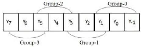
Considering the first 3 bits of Y, we can determine whether to add X, 2X or 0 to partial product. The grouping of Y bits is shown in fig.
Fig 2: Multiplier bit grouping according to Modified Booth Encoding
Modified Booth Multiplier
Block diagram of the Modified Booth multiplier is shown in fig. This circuit takes two 8-bit binary numbers and produces the 16-bit product. Multiplier, X[7:0], is divided into the four groups: 0, X0, X1; X1, X2, X3; X3, X4, X5; X5, X6, X7.
Fig3 : Modified Booth Multiplier
Copyright to IJIRCCE DOI: 10.15680/IJIRCCE.2017. 0506084 11482
partial products only to four, which significantly improving speed. Also, the CLA provides boost to the speed of the system.
Urdhva Triyagbhyam Multiplier
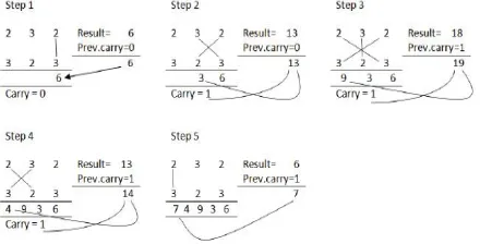
"Urdhva" and "Tiryagbhyam" words are derived from Sanskrit literature. Urdhva means "Vertically" and Tiryagbhyam means "crosswise". It is based on a novel concept, where the generation of all the partial products can be performed with concurrent addition of partial products. Anyone can easily realize that this Vedic method makes difference for the mental calculations. Also, for the mental calculations it was proved more convenient, as it can be easily visualize the Vedic multiplication line diagram which is shown in the figure. If somebody tries to calculate multiplication mentally in the conventional method, one would have to memorize first row, then the second row and likewise; thereafter add all of them.
Fig 4 : Line diagram for multiplication of two 4-bit numbers
A simple example shown in figure, the digits on the two ends of the line are multiplied and the result is added with the prior carry. When there are more lines in the one step; and all the outcomes are added to previous carry. The least significant digit of the number thus obtained acts as one of the result digits and the rest act as the carry for the next step. In the beginning the carry was taken to be zero.
Fig 5 : Multiplication of 232 × 323=74936 by Urdhva Tiryagbhyam sutra with line diagram
Copyright to IJIRCCE DOI: 10.15680/IJIRCCE.2017. 0506084 11483
4-BIT MULTIPLIER
After designing 2 x 2 multiplier, 4-bit multiplier is also designed using wallace tree method as shown in fig.
Fig 6 : 4 Bit Multiplier
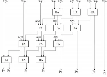
8-BIT MULTIPLIER
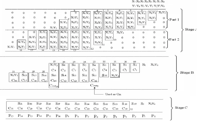
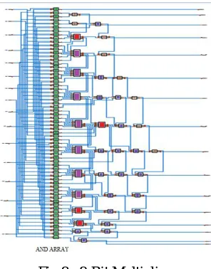
8x8 bit multiplier architecture based on Wallace Tree is shown, which is efficient in terms of the power and the regularity without increase in the delay and area. The idea involves generation of partial products in the parallel using the AND gates. Furthermore, the addition of the partial products is done using the Wallace tree, which is hierarchal, divided into levels. There will be a reduction in power consumption, since the power is provided only to level that is involved in the computation. Hardware realization of 8 x 8 multiplier is shown.
Copyright to IJIRCCE DOI: 10.15680/IJIRCCE.2017. 0506084 11484
Schematic diagram of GDI based 8 x 8 multiplier is shown in fig.
Fig 8 : 8-Bit Multiplier
III.SIMULATION RESULT AND ANALYSIS
This paper shows Simulation results of all the building blocks. Functional verification of a design can be done by using simulation based verification. This verification ensures that the design is functionally correct when tested with a given set of inputs. Each method waveform is compared for Power Calculation, Delay Calculation and Area in terms of Transistor and the design has been implemented and simulated using Tanner Tool in 180nm technology with Operating voltage of approximately 1.8V
4-BIT MULTIPLIER
Simulated waveform of 4-bit GDI based multiplier is shown. Multiplier and multiplicand inputs each are of 4 bits. After multiplication 8-bit partial products are generated. Here both CMOS and GDI based 4 x 4 multiplier are designed and analysed. GDI based multiplier gives better results in terms of propagation delay, power dissipation and area by using transistor count.
Fig 9: Waveform of 4-bit GDI based Multiplier
Copyright to IJIRCCE DOI: 10.15680/IJIRCCE.2017. 0506084 11485
Table 2
Parameter of 4-bit CMOS multiplier
Vdd (V) Delay (ns) Power Dissipation (mW)
1.8 0.185 5.7252
1.6 0.225 4.4303
1.4 0.289 2.6030
1.2 0.359 1.5436
1.0 0.411 0.7801
Table 3
Parameter of 4-bit GDI multiplier
Vdd (V) Delay (ns) Power Dissipation (mW)
1.8 0.012 5.6982
1.6 0.056 4.2103
1.4 0.075 2.3864
1.2 0.195 1.3488
1.0 0.278 0.6865
IV.COMPARISON
Comparison of propagation delay, power dissipation and area between CMOS multiplier and GDI multiplieris summarized in this section.
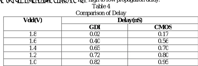
COMPARISON OF DELAY
Comparison of delay between 8-bit CMOS multiplier and 8-bit GDI multiplier is given in table at different supply voltage.
Delay of circuit is calculated by using given formula
2
PHL PLH
Delay
Where τPLH is Low to high propagation delay and τPHL high to low propagation delay. Table 4
Comparison of Delay
Vdd(V) Delay(nS)
GDI CMOS
1.8 0.02 0.17
1.6 0.40 0.56
1.4 0.65 0.70
1.2 0.72 0.80
1.0 0.82 0.95
Copyright to IJIRCCE DOI: 10.15680/IJIRCCE.2017. 0506084 11486
Fig 10: Comparison of Delay at different supply
V.CONCLUSION
Multiplier is one of the most important components of many digital signal processing, general The GDI based wallace tree multiplier occupies smaller silicon area with higher resolution than the conventional wallace tree multiplier. Various parameters like delay and power dissipation of other circuits are also calculated with respect to different power supply. Result shows that Power dissipation and delay of GDI based Wallace tree multiplier at 1.8V power supply is 8.8mW and 0.02 nS respectively and total transistor count is 912.
Although some aspects of the goal have been achieved using this design, but still a better wallace tree multiplier can be made by some improvement in the circuit design. The wallace tree multiplier can be further extended and modified by the following points.
REFERENCES
[1] Jin -Hao Tu and Lan-Da Van, (2009) “Power –Efficient Pipelined Reconfigurable Fixed -Width Baugh-Wooley Multipliers”. IEEE TRANSACTIONS ON COMPUTERS, OCT, OL.58, No.10, pp.1346-1355.
[2] Abhijit Asati and Chandrashekhar,(2008) “An Improved High Speed fully pipelined 500 MHz 8 x 8 Baugh Wooley Multiplier design using 0.6
μm CMOS TSPC Logic Design Style”. IEEE, Colloquium and the Third ICIIS, Dec, pp.1-6.
[3] Abhishek Mukherjee and Abhijit Asati, (2013) “Generic Modified Baugh Wooley Multiplier”. IEEE, International Conference on Circuits, Power and Computing Technologies, March, pp.746-751.
[4] Steve Hung-Lung Tu and Chih-Hung Yen, (2006) “A High-Speed Baugh-Wooley Multiplier Design Using Skew - Tolerant Domino Techniques” . IEEE, APCCAS, pp. 598 -601.
[5] Rakesh Warrier, C.H. Vun and Wei Zhang, (2014) “A Low-Power Pipelined MAC Architecture using Baugh- Wooley based Multiplier”. IEEE, Global Conference on Consumer Electronics, pp. 505-506.
[6] Kelly Liew Suet Swee and Lo Hai Hang, (2012) “Performance Comparison Review of 32-Bit Multiplier Designs”. IEEE, International Conference on Intelligent and Advanced Systems, pp. 836 - 841.
[7] Amir Khatibzadeh and Kaamran Raahemifar, (2005) “A Novel Design of a 6- GHz 8x8 pipelined Multiplier”. IEEE, International Database Engineering and Application Symposium (IDEAS‟05).
[8] Aiman Badawi, Ali Alqarni, Abdullah Aljuffri, Mohammed S. Bensaleh, Abdulfattah M. Obeid and Syed Manzoor Qasim, (2015) “FPGA Realization and Performance Evaluation of Fixed- Width Modified Baugh - Wooley Multiplier”. IEEE, pp. 155 - 158.