Vol. 5, Issue 6, June 2017
Design and Analysis of 8 X 8 Wallace Tree
Multiplier using GDI and CMOS Technology
Pradeep Kumar Kumawat, Gajendra Sujediya Research Scholar, Department of EC, RIET, Jaipur, India
Assistant Professor, Department of EC, RIET, Jaipur, India
ABSTRACT: Multiplier is an arithmetic circuit that is extensively used in DSP, microprocessors and communication applications like, FFT, Digital Filters etc. Today entire world is demanding compact and small digital devices which should perform fast with low power consumption. Multiplier is the basic building block in almost all digital devices and it impacts the speed, power and area of a device significantly. Thus it is important to design an efficient multiplier which should perform fast with low power consumption. Optimizing the delay, area and power of a multiplier is a major design issues, as area and speed are usually conflicting constraints.
I.INTRODUCTION
With expeditious development of VLSI applications such as DSP, image, video processing and microprocessors extensively use logic gates and arithmetic circuits. Because of powered by batteries, the supply voltage is often limited, and the life time of the battery is of great importance for these devices. Therefore,. With the scaling down of VLSI technologies, more complicate digital circuits have been implemented with a higher clock rate and lower supply voltage. However, the decreased supply voltage restricts the signal swing in circuits and brings difficulties for circuit design. .
II.BASICS OF MULTIPLIERS
Multiplication is an operation that occurs frequently in digital signal processing and many other applications. However, multipliers occupy a much larger area and incur much longer delays than adders. Therefore it is imperative that special techniques be used to speed up the calculation of the product while maintaining a reasonable area.
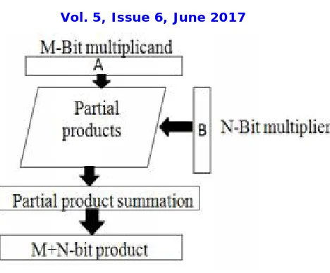
The product is the outcome of multiplying the multiplicand to multiplier. Multiplication operation is performed using two main steps. First is partial product formation that consists of the AND-ing each bit of multiplier with multiplicand. Each consecutive partial product belongs to one place to left of the previous partial product. Second step is the partial product accumulation step, where partial products are merged to form the result.
Basic Multiplication Process
ISSN(Online): 2320-9801
ISSN (Print): 2320-9798
I
nternational
J
ournal of
I
nnovative
R
esearch in
C
omputer
and
C
ommunication
E
ngineering
(An ISO 3297: 2007 Certified Organization)
Website: www.ijircce.com
Vol. 5, Issue 6, June 2017
Fig 1: Generic Multiplier Block Diagram
The most basic form of the multiplication consists of forming product of the two unsigned (positive) binary number. This can be accomplished through traditional technique simplified to radix 2.
1011 (this is 11 in binary)
× 1011 (this is 11 in binary)
==========
1011 (1011 × 1)
1011 (1011 × 1, shifted one position to the left)
0000 (1011 × 0, shifted two positions to the left)
+1011 (1011 × 1, shifted three positions to left)
===========
01111001 (this is 121 in binary)
The above example shows the multiplication process of two unsigned binary digits. The first digit is called Multiplicand and the second one is Multiplier. Partial product generation is the very first step in binary multiplier. If the multiplier bit is “0”, then partial product row is also zero, and if it is “1”, then the multiplicand is copied as it is. From the 2nd bit multiplication onwards, each partial product row is shifted one unit to the left as shown in the above mentioned example.
Multiplication involves two basic operations:
Generation of the partial product
Their accumulation
Partial Product Generation Method
Vol. 5, Issue 6, June 2017
Fig 2 : Generation logic of partial product
There are two ways to improve the speed of multiplication operation.
Speed up the process of partial products generation.
Reduce the number of partial products that needs to be generated.
The first option can be achieved by using different architecture for partial product generation. Considering if a bit is generated with just an AND gate delay, it seems that the partial product bits are already calculated in the fastest way possible. AND operation is equivalent to multiplication on two numbers. The second option will most likely take longer than an AND gate, but it reduces the number of partial product results in a smaller tree and save the time of partial product generation Thus it would be beneficial to implement this option..
Wallace/ Dadda Multiplier
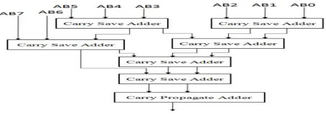
The speed of multiplier is depends on the total time taken for summation of partial products. Scientist C. S. Wallace introduced an effective way of summing the partial product bits in the parallel using the tree of the Carry Save Adders which generally known as the “Wallace Tree”.
Wallace trees are irregular in the sense that the informal description does not specify a systematic method for the compressor interconnections. However, it is an efficient implementation of adding partial products in parallel. A typical Wallace tree architecture is shown in figure.
Fig 3 : Wallace multiplier
Wallace method used three steps to multiply two numbers. These steps are
ISSN(Online): 2320-9801
ISSN (Print): 2320-9798
I
nternational
J
ournal of
I
nnovative
R
esearch in
C
omputer
and
C
ommunication
E
ngineering
(An ISO 3297: 2007 Certified Organization)
Website: www.ijircce.com
Vol. 5, Issue 6, June 2017
Bit product matrix is “reduced” into two row matrix by using the carry-save adder (also called 3:2 counters).
The remaining two rows are summed by using the fast carry-propagate adder to produce the final product. Although
this may seem to be a complex process, it yields the multipliers with delay proportional to logarithm of operand size n. This algorithm reduced the partial product at a rate of log3/2 N/2. By using carry-save adder the need of carry propagation in the adder is avoided and latency of one addition is equal to gate delay of adder.
III.DESIGN OF CIRCUIT
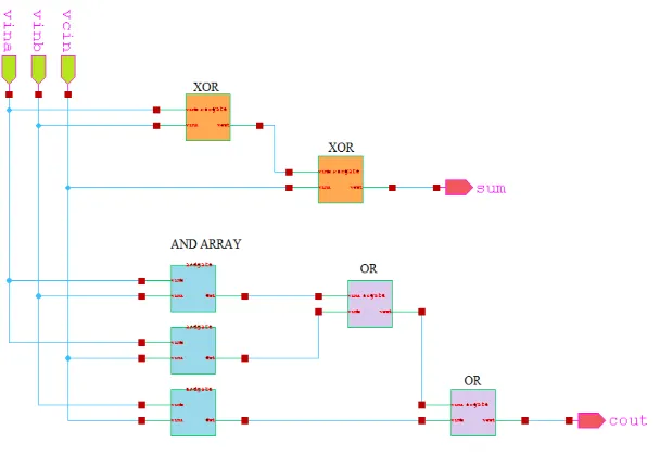
FULL ADDER GDI
Schematic diagram of GDI based full adder circuit is shown in figIt is used to add three inputs vina, vbin and vcin to
produce sum and carry out (cout). Vcin input is the carry generated from previous stage.
Fig 4 : GDI Based full adder
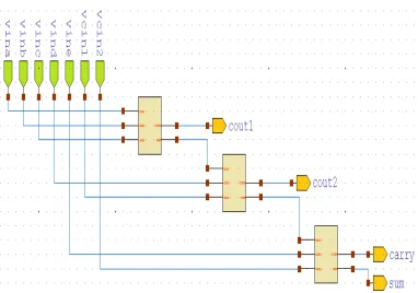
COMPRESSOR
Vol. 5, Issue 6, June 2017
Fig 5: 4 to 2 Compressor
Fig 6 : 5 to 2 Compressor
IV.SIMULATION RESULT AND ANALYSIS
ISSN(Online): 2320-9801
ISSN (Print): 2320-9798
I
nternational
J
ournal of
I
nnovative
R
esearch in
C
omputer
and
C
ommunication
E
ngineering
(An ISO 3297: 2007 Certified Organization)
Website: www.ijircce.com
Vol. 5, Issue 6, June 2017
FULL ADDER
Simulated waveform of GDI based full adder is shown in fig. It has three inputs and two outputs sum and carry out & used for addition of three inputs. Its working is same as half adder.
Fig 7 : Waveform of Full adder
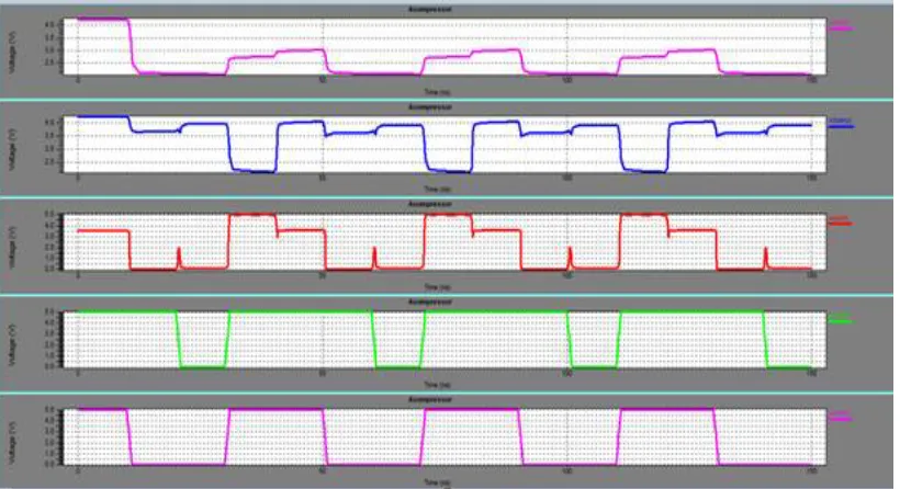
COMPRESSOR
Compressor is a special types of adder used to add more than three inputs. Simulated waveform of 4-2 compressor and 5-2 compressor is shown in fig respectively.
Vol. 5, Issue 6, June 2017
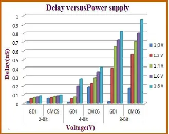
Fig 9: Comparison of Delay at different supply
V.CONCLUSION
Multiplier is one of the most important components of many digital signal processing, general purpose processing, image processing and other digital application. Multiplier performance can be measured by using performance factors like Power, Delay and area. In efforts to identify the most efficient multiplier, this research makes the following conclusions.
The GDI based wallace tree multiplier occupies smaller silicon area with higher resolution than the conventional wallace tree multiplier. Various parameters like delay and power dissipation of other circuits are also calculated with respect to different power supply. Result shows that Power dissipation and delay of GDI based Wallace tree multiplier at 1.8V power supply is 8.8mW and 0.02 nS respectively and total transistor count is 912.
REFERENCES
[1]. C. S. Wallace, A Suggestion for a Fast Multiplier, IEEE Transactions on Computers, 13, 1964,14-17
[2].E. E. Swartzlander, and R. S. Waters, A Reduced Complexity Wallace Multiplier Reduction, IEEE Transactionson Computers, 59, 2010, 1134-1137.
[3].M. Kumar, M. A. Hussain, and S. K. Paul, Performance of a Two Input Nand Gate Using Subthreshold Leakage Control Techniques, Journal of Electron Devices, 14, 2012, 1161 -
1169.
[4]. M. Kumar, M. A. Hussain, and L. K. Singh, Design of a Low Power High Speed ALU in 45nm Using GDI Technique and its Performance Comparison, Communications in omputer and Information Science, Springer Berlin Heidelberg, 142, 2011,458-463.
[5].P.V. Rao, C. P. R. Prasanna, and S. Ravi, VLSI Design and Analysis of Multipliers for Low Power, IEEE Fifth International Conference on Intelligent Information Hiding and Multimedia Signal Processing, Kyoto,2009,1354-1357.
[6]. D. R. Gandhi, and N. N. Shah, Comparative Analysis for Hardware Circuit Architecture of Wallace Tree Multiplier, IEEE International Conference on Intelligent Systems and Signal Processing, Gujarat, 2013,1-6