most needed factors. In any high speed circuits, Static Random Access Memories (SRAMs) has been most usually used information storage devices. In the proposed paper work, a concurrent BIST Architecture ave been used for monitoring the set of input vectors during the normal operation of SRAM. A low power consumption is made possible than the previously used system.
Keywords—storage devices, BIST, Fault coverage.
INTRODUCTION
For semiconductor integrated circuits, during the past decades, the CMOS technology emerged as the dominant fabrication method, and CMOS became the almost exclusive choice for semiconductor memory design also. Device scaling has resulted in large scale integrated, high performance, low-power, and low cost systems. CMOS memories are used in a much greater quantity than all the other types of semiconductor integrated circuits, and appear in an astounding variety of circuit organizations. With the development of CMOS memory technology numerous publications presented select memory circuit and architecture designs. [1]The literature of CMOS technology made little effort to give overview methodical analyses of some significant memory specific issues such as sense amplifiers, redundancy implementations and radiation hardening by circuit technical approaches.
Figure 1. Elementary SRAM structure
[7]Due to CMOS technology scaling and the need of battery operated devices continues to drive the increase of on-die memory density to meet performance needs in various applications. Meanwhile, the device variation and leakage are increasing as the miniaturization of the transistor continues which also affects the reliability and performance of the device. As a result, it is increasingly challenging to develop SRAM with adequate stability margin for low-voltage operation while keeping the power consumption low enough to meet system-level power requirements. It is analyzed the performance of various topologies of SRAM cells at various process technologies for enhancing the cell stability which is related to the cell SNM and the leakage power consumption.
II. PROPOSED 7T SRAM CELL WITH THE BIST SCHEME
Context below explains the working of 7T SRAM cell comprising the read, write operations, considering the performance of the device also obtaining the performance comparison with the CMOS SRAM cell.
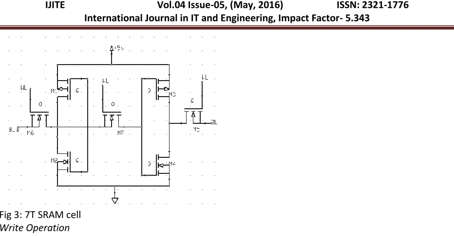
The circuit of 7T SRAM cell consists of two inverters that are connected and cross coupled to each other with additional NMOS transistor which connected to write line (WL) and also having two pass NMOS transistors connected to bit lines (BL) and bit-lines bar (BLB) respectively. Figure 3 shows circuit of 7T SRAM Cell, where the access transistor M6 is connected to the word-line (WL) which will perform the access write and M3 is connected to the Read-line (R) to perform the read operations. Bit-lines will act as the I/O nodes carrying data from SRAM cells to a sense amplifier during read operation, or from the write input in the memory cells during write operations.
Fig 3: 7T SRAM cell Write Operation
*4+The 7T SRAM cell’s write operation starts by turning M7 off this in turn will cut off the feedback connection. BLB signal carries the complement of the input data, Q6 is turned on, while is off as shown in Figure 4. The 7T SRAM cell looks here like two cascaded inverters connected in series as shown in Figure 4. M6 is the transistor which transfers the data from BLB to which drives second set of inverters, M3 and M4, to develop the cell data.
Figure 4: Write operation circuit.
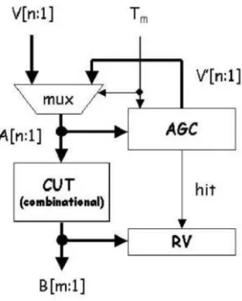
Let us consider a combinational CUT with n input lines, from the figure 6; hence the possible input vectors for this CUT are 2n. The proposed scheme is based on the idea of monitoring a window of vectors, whose size is W, with W = 2w, where w is an integer number w < n.
Figure 6: proposed architecture.
Every moment, the test vectors belonging to the window are monitored, and if a vector performs a hit, the RV is enabled. Proposed architecture is shown in figure 6. [5]The bits of the input vector are separated into two distinct sets comprising w and k bits, respectively, such that w + k = n. The k (high order) bits of the input vector show whether the input vector belongs to the window under consideration. The remaining bits show the relative location of the incoming vector in the current window. If the incoming vector belongs to the current window and has not been received during the examination of the current window, we say that the vector has performed a hit and the RV is clocked to capture the CUT’s response to the vector. When all vectors that belong to the current window have reached the CUT inputs, we proceed to examine the next window.
response verifier enable (rve) signal. During the second half of the clock cycle, the left flip-flop (the one whose clock input is inverted)enables the AND gate (whose other input is clk and cmp), and enables the buffers to write the value one to the addressed cell.
IV SIMULATION AND RESULTS
The proposed Architecture circuits have been simulated using Xilinx13.2 tool. Also we have used ModelSim SE as a verification tool which provides High Performance Simulation and Debug. ModelSim SE is our UNIX, Linux, and Windows-based simulation and debug environment, combining high performance with the most powerful and intuitive GUI in the industry.
Figure 7: Logic module
XilinxISE (Integrated Software Environment) is a software tool produced by Xilinx for synthesis and analysis of HDL designs, enabling the developer to synthesize (compile) their designs, perform timing analysis, examine RTL diagrams, simulate a design's reaction to different stimuli, and configure the target device with the programmer.
During the write cycle the operation consumes power of 0.7µW with the consumption of 0.5µA. the read operation for each cell requires 0.06µW of power and 0.10µA of current.
Nikhil Saxena*2, Nikhita Tripathi*3International Journal of Engineering Trends and Technology (IJETT) Volume4Issue5- May 2013
[2]. Voyiatzis, A. Paschalis, D. Gizopoulos, N. Kranitis, and C.Halatsis, “A concurrent BIST architecture based on a selftestingRAM,” IEEE Trans. Rel., vol. 54, no. 1, pp. 69–78,Mar. 2005.
[3] E. J. McCluskey, “Built-in self-test techniques,” IEEE Design TestComput., vol. 2, no. 2, pp. 21–28, Apr. 1985.
[4] SNM Analysis During Read Operation Of 7T SRAM Cells In 45nm Technology For Increase Cell Stability Deependra Singh Rajput, Manoj Kumar Yadav, Pooja Johri, Amit S. Rajput, International Journal of Engineering Research and Applications (IJERA) ISSN: 2248-9622 www.ijera.com Vol. 2, Issue4, July-August 2012, pp.2112-2117