987 | P a g e
Implementation of Current Sensorless Dual-Boost Half
Bridge Digital PFC Converter with Capacitor Voltage
Balancing Condition
Ms. Gangurde Charushila K.
1, Prof. Agnihotri S.P.
2.
1
Student,
2Head
Department of Electronics & Telecommunication Engineering,
GES’ RHSCOEMS &R Nashik, Maharashtra (India)
ABSTRACT
The Power Factor Correction (PFC) converters of bridgeless category are often used to improve the efficiency of the conventional boost-type power factor correction (PFC) converters with the diode bridge circuit. The short circuit problems are not occurred due to non-in ability of series connected switches for improving PFC Dual boost Half-bridge circuit is used. The DBHB PFC converter model is developed in added to simplified the conventional two loop Control scheme and reduce the number of current sensors. Then, the current sensor-less control for DBHB PFC converter is proposed to achieve voltage regulation and yield sinusoidal input current in phase with the input voltage without sensing any current. In addition, the proposed method is able to balance capacitor voltages naturally without adding any voltage balancing control loop. The above maintain method we proposed for observing the performance of the DBHB PFC planning to design in Matlab/Simulation and planning for experimental setup.
Keyword
: -
Boost Converter, Dual Boost Half Bridge (DBHB), Insulated Gate Bipolar Transistor
(IGBT), Power factor, Power Factor Correction (PFC) converter.
1. INTRODUCTION
In order to reduce the power transmission loss and improve the power quality, more and more electronic
products are required to include the power factor correction (PFC) function. The conventional PFC function is
often implemented in the circuit topology a diode bridge rectifier with a single-switch boost converter . This
topology is simple, but it suffers from larger conduction voltage drop and switch power loss than other
topologies, such as half-bridge PFC converter , full-bridge converter , and the bridgeless PFC converters. The
Power Factor Correction (PFC) converters of bridgeless category are often used to improve the efficiency of the
conventional boost-type power factor correction (PFC) converters with the diode bridge circuit. Due to no
series-connected switches and no short-through risks, the dual-boost half-bridge (DBHB) circuit is used as the
PFC converter. Then, the current sensor less control for DBHB PFC converter is proposed to achieve voltage
988 | P a g e
1.1 Power Factor:-Power factor is defined as the cosine of the angle between voltage and current in an ac circuit. There is
generally a phase difference Ø between voltage and current in an ac circuit. cos Ø is called the power factor of
the circuit. If the circuit is inductive, the current lags behind the voltage and power factor is referred to as
lagging. However, in a capacitive circuit, current leads the voltage and the power factor is said to be leading.
In a circuit, for an input voltage V and a line current I,
1) VIcos Ø –the active or real power in watts or kW.
2) VIsin Ø- the reactive power in VAR or kVAR.
3) VI- the apparent power in VA or kVA.
Power Factor gives a measure of how effective the real power utilization of the system is. It is a measure of
distortion of the line voltage and the line current and the phase shift between them. Power Factor=Real power
(Average)/Apparent power. Where, the apparent power is defined as the product of rms value of voltage and
current.
1.1.1 Linear System:-
In a linear system, the load draws purely sinusoidal current and voltage; hence the power factor is determined
only by the phase difference between voltage and current .i.e. PF=cos
1.2 Power Factor Correction:-
Power factor correction is the term given to a technology that has been used since the turn of the 20th century to
restore the power factor to as close to unity as is economically viable. This is normally achieved by the addition
of capacitors to the electrical network which compensate for the reactive power demand of the inductive load
and thus reduce the burden on the supply. There should be no effect on the operation of the equipment.
1.2.1 Types of Power Factor Correction:-
A) Passive Power Factor Correction (PFC):-
Harmonic current can be controlled in the simplest way by using a filter that passes current only at line
frequency (50 or 60 Hz).Harmonic currents are suppressed and the non-linear device looks like a linear load.
Power factor can be improved by using capacitors and inductors i.e. passive devices. Such filters with passive
devices are called passive filters.
Disadvantage:-They require large value high current inductors which are expensive and bulky. A passive PFC
circuit requires only a few components to increase efficiency, but they are large due to operating at the line
power frequency.
B) Active Power Factor Correction (PFC) :-
An active approach is the most effective way to correct power factor of electronic supplies. Here, we place a
boost converter between the bridge rectifier and the main input capacitors. The converter tries to maintain a
constant DC output bus voltage and draws a current that is in phase with and at the same frequency as the line
989 | P a g e
II. BOOST CONVERTER & IGBT
2.1 Principle of Step-Up Operation (Boost Converter):-
The circuit diagram of a step up operation of Boost Converter is shown in Figure 2.1.The output voltage is
always greater than the input voltage. When the switch is closed for time duration, the inductor current rises and
the energy is stored in the inductor. If the switch is opened for time duration, the energy stored in the inductor is
transferred to the load via the diode and the inductor current falls.
Fig.2.1:- General Configuration of a Boost Converter
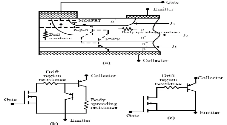
2.2 Operating principle of an IGBT:-
Operating principle of an IGBT can be explained in terms of the schematic cell structure and equivalent circuit
of Fig 2.2(a) and (c). From the input side the IGBT behaves essentially as a MOSFET. Therefore, when the gate
emitter voltage is less then the threshold voltage no inversion layer is formed in the p type body region and the
device is in the off state. The forward voltage applied between the collector and the emitter drops almost entirely
across the junction J
2. Very small leakage current flows through the device under this condition. In terms of the
equivalent current of Fig 2.2(c), when the gate emitter voltage is lower than the threshold voltage the driving
MOSFET of the Darlington configuration remains off and hence the output p-n-p transistor also remains off.
Fig.2.2:-Parasitic thyristor in an IGBT cell. a) Schematic Structure , b) Exact
990 | P a g e
When the gate emitter voltage exceeds the threshold, an inversion layer forms in the p type body region under
the gate. This inversion layer (channel) shorts the emitter and the drain drift layer and an electron current flow
from the emitter through this channel to the drain drift region. This in turn causes substantial hole injection from
the p+ type collector to the drain drift region. A portion of these holes recombines with the electrons arriving at
the drain drift region through the channel. The rest of the holes cross the drift region to reach the p type body
where they are collected by the source metallization.From the above discussion it is clear that the n type drain
drift region acts as the base of the output p-n-p transistor. The doping level and the thickness of this layer
determine the current gain “∝” of the p-n-p transistor. This is intentionally kept low so that most of the device current flows through the MOSFET and not the output p-n-p transistor collector. This helps to reduced the
voltage drop across the “body” spreading resistance shown in Fig 2.2 (b) and eliminate the possibility of static
latch up of the IGBT.
The total on state voltage drop across a conducting IGBT has three components. The voltage drop across J
1
follows the usual exponential law of a pn junction. The next component of the voltage drop is due to the drain
drift region resistance. This component in an IGBT is considerably lower compared to a MOSFET due to strong
conductivity modulation by the injected minority carriers from the collector. This is the main reason for reduced
voltage drop across an IGBT compared to an equivalent MOSFET. The last component of the voltage drop
across an IGBT is due to the channel resistance and its magnitude is equal to that of a comparable MOSFET.
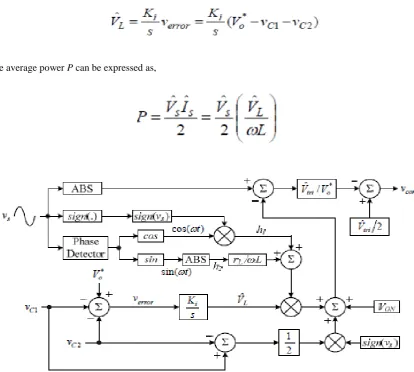
III. PROPOSED CURRENT SENSORLESS CONTROL:-
In order to reduce the current sensor, the single-loop current sensor-less control is proposed. The proposed
current sensor-less control is able to regulate the output voltage Vo and shape the input current is in phase with
the input voltage vs . For the PFC function, the desired average current can be expressed as the sin(t) function
Therefore, the average inductor voltage <vL>Ts should be
forced to the cos(t) expression
where the value VˆL =LIˆs can be seen as the amplitude of the inductor voltage <vL>Ts . The control signal
991 | P a g e
where . is the absolute (ABS) operator and the terms h1 = cos(t) sign(vs ) and h2 = sin(t)areSynchronously generated from the input voltage vs .The proposed current sensor-less control scheme is plotted
in Fig. 4.1. A simple integrator controller is used to regulate the output voltage and tune the voltage signal VˆL .
The average power P can be expressed as,
Fig. 3.1:- Proposed current sensorless control scheme.
992 | P a g e
is determined from the difference between the output voltage Vo and the voltage command Vo through an integrator controller. The voltage error verror in the imbalanced condition can be approximated aswhere Verror is the dc voltage error and the line-frequency component is dominant ripple. After the integrator
controller with gain Ki , the controller output VˆL.
where 0 ˆVL is the dc value of VˆL .
The small-signal transfer function between the output voltage ∆Vo and the controller output ∆VˆL can
be obtained from the power balance between the input power Ps , the load power PR and two capacitor powers
PC1 , PC2 . The input power Ps with small perturbation ∆Ps can be expressed as
The load power PR with small perturbation ∆PR can be represented by the voltage command Vo̽ plus the output voltage perturbation ∆Vo .
The two capacitor power perturbations ∆PC1 and ∆PC2 can be depicted by the output voltage perturbation ∆Vo
, respectively.
Hence, Small transfer signal function gain is
993 | P a g e
The block diagram closed-loop voltage control shows in fig. 4.2.Fig.3.2:-Block diagram of closed-loop voltage control.
IV.
SIMULATION RESULT AND DISCUSSION
In this section, some simulation results of the proposed current sensor-less control for dual-boost half-bridge
PFC converter are provided. The simulation parameters and some nominal values are listed in Table I. The
root-mean-square (rms) value of input voltage vs is 110 V and the line frequency f is 50 Hz. The voltage controller is a simple integrator which is used to tune the controller output VˆL .
A .Steady State Response:-
The steady-state waveforms with the output power 400W and 800W respectively. It is found that the input
currentis sinusoidal in phase with the input voltage vs . Moreover, the output voltage Vo is well regulated to the voltage command Vo ̽ = 400V, and both output capacitor voltages Vc1 and Vc2 are well balanced at 200V. Obviously, significant line-frequency components can be found in each capacitor voltage, but only double-line
994 | P a g e
TABLE 1. SIMULATION PARAMETERS
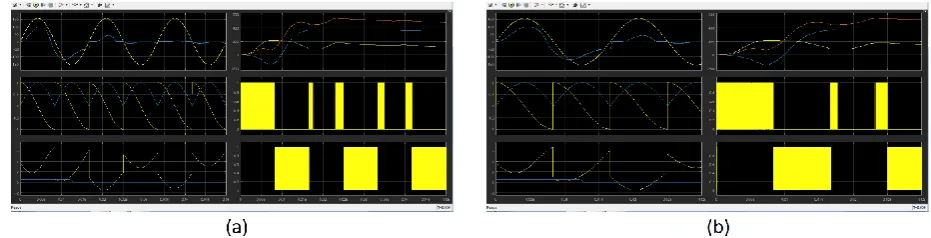
B. Transient
Response:-In order to evaluate the transient responses of the proposed current sensor-less control, the load resistor is
changed between 400Ω and 200Ω. Some simulation results are plotted in Fig. 4.2.The yielded input current is is
still sinusoidal in phase with the input voltage vs , and the output voltage Vo is stably regulated back to 400V during the change of the load resistor. Thus, the simple integrator controller included in the voltage loop is able
to regulate the output voltage.
Fig.4.2.Simulation results when the load resistor changes: (a) from Resistive Load=400Ω to 200Ω
(b) from Resistive Load=200Ω to 400Ω, L Load=2mH.
Input voltage Vs = 11oV
Output Voltage Command Vo ̽ = 400V
Switching Frequency fs = 45kHz
Line Frequency f=50Hz
Inductances LA = LB = 2 mH
Inductor resistances rLA =rLB = 0.4Ω
Capacitance C1 = C2 = 1170μF
Capacitance voltage VON = 2V
995 | P a g e
C. Capacitor voltage Balancing:-The simulation results are plotted in Fig.4.3 (a) It can be found that the capacitor voltage vC1 gradually drops
down to 155V, and the other capacitor voltage vC2 rises up to near 245V simultaneously due to the proposed
current sensor-less control. In Fig. 4.3 (b), the extra 100Ω resistor is suddenly connected to the capacitor C2 .
The capacitor voltages vC1 and vC2 gradually fluctuate to 245V and 155V, respectively, but the output voltage Vo
is regulated to 400V.
Fig.4.3:-Simulation results when a 100Ω resistor is connected to (a) the capacitor C1 original waveforms; (b) the capacitor C2 original waveforms.
V. CONCLUSION
The single-switch model for Dual-Boost Half Bridge (DBHB) PFC converter has been developed. The current
sensor-less control method for DBHB PFC converter has been proposed and implemented in this paper. To gain
the efficiency over the conventional boost type power factor correction (PFC) converters with the diode bridge,
We use the Power Factor Correction (PFC) converters of bridgeless category. The short circuit problems are not
occurred due to non inability of series connected switches for improving PFC Dual boost Half-bridge circuit is
used. The DBHB PFC converter model is developed in added to simplified the conventional two loop control
scheme and reduces the number of current sensors. The integrator-type voltage controller is able to regulate the
output voltage and balance the capacitor voltages. The proposed control strategy effectively achieves PFC
function in steady-state condition and transient condition. Moreover, the capacitor voltages can be naturally
balanced by the proposed control method. This control method can be used to the half-bridge PFC converter due
to the same single-switch model.
VI. ACKNOWLEDGEMENT
First and the foremost I, take this opportunity to express gratitude to my guide, Mr. S. P. Agnihotri, for his
constant encouragement and support throughout the project implementation. I sincerely thank Prof. S. P.
Agnihotri, Head of Department of Electronics & Telecommunication Engineering for his advice and support
996 | P a g e
With deep sense of gratitude I thank to our Principal Dr. P. C. Kulkarni and Management of GokhaleEducation Society for providing all necessary facilities and their constant encouragement and support. I also
express my thanks to all teaching and non-teaching staff for their kind co-operation and guidance also.
REFERENCES
[1]. R. Srinivasan and R. Oruganti, “A Unity Power Factor Converter Using Half-Bridge Boost Topology,”
IEEE Trans. Power Electron, vol. 13, May 1998.
[2]. Liu and K. Smedley, “Control of a Dual Boost Power Factor Corrector for High Power Applications,” in
Proc. IEEE IECON, 2003.
[3]. M. H. Rashid, Power Electronics: Circuits, Devices and Applications, 3rd edition, Pearson, 2004
[4]. M. Chen and J. Sun, “Feed-forward Current Control of Boost Single-Phase PFC Converters,” IEEE Trans.
Power Electron, vol. 21, Feb. 2006.
[5]. R. Ghosh and G. Narayanan, “A Simple Analog Controller for Single-Phase Half-Bridge Rectifier,” IEEE
Trans. Power Electron, vol. 22, Jan. 2007.
[6]. H. C. Chen, H. Y. Li and R. S. Yang, “Phase Feed-forward Control for Single-Phase Boost-Type SMR,”
IEEE Trans. Power Electron. vol. 24, May 2009.
[7]. T. Qi, L. Xing, and J. Sun, “Dual-Boost Single-Phase PFC Input Current Control Based on Output Current
Sensing,” IEEE Trans. Power Electron, vol. 24, Nov. 2009.
[8]. F. J. Azcondo, and A. de Castro, V. M. Lopez, and O. Garcia, “Power Factor Correction without Current
Sensor Based on Digital Current Rebuilding,” IEEE Trans. on Power Electronics, vol. 25, Jan. 2010.
[9]. J. M. Wang, S. T. Wu, Y. Jiang, and H. J. Chiu, “A Dual-Mode for the Boost PFC Converter,” IEEE Trans.
Ind. Electron., vol. 58, Jan. 2011.
[10].S. M. Park, Y. D. Lee, and S. Y. Park, “Voltage Sensor-less Feed-forward Control of a Dual Boost PFC
Converter for Battery Charger Applications,” in Proc. Energy Convers. Cong. Expo. (ECCE), 2011.
[11].H. C. Chen, C. C. Lin, and J. Y. Liao, “Modified Loop Current Sensor-less Control for
Single-Phase Boost-Type SMR With Distorted Input Voltage,” IEEE Trans. Power Electron., vol. 26, May 2011.
[12].P. Fang and Y. F. Liu, “A Innovative Current Sensor-less Continuous Conduction Mode PFC Control,” in
Proc. IEEE ECCE Conf., 2013.
[13].H. C. Chen, and J. Y Liao, “Bidirectional Current Sensor-less Control for Full-Bridge AC/DC Converter
with Considering Both Inductor Resistance and Conduction Voltages,” IEEE Trans. on Power Electronics,
vol. 29, 2013.
[14].Edison R. C. da Silva and Malik E. Elbuluk, Fundamentals of Power Electronics chapter(2) “Power
electronics for renewable and distributed energy system”.Springer international publishing,2013
[15].V. M. Lopez, F. J. Azcondo, and A. de Castro, and R. Zane, “Universal Digital Controller for Boost CCM
Power Factor Correction Stages Based on Current Rebuilding Concept,” IEEE Trans. on Power
Electronics, vol. 29, July 2014.
[16].K. I. Hwu, Y. T. Yau, and Y. C. Chang, “Full-Digital AC/DC Converter with PFC Based on Counting,”
997 | P a g e
[17].H. H. Shin, H. Cha, H. G. Kim, D. W. Yoo, “Novel Single-Phase PWM AC–AC Converters Solving
Commutation Problem Using Switching Cell Structure and Coupled Inductor,” IEEE Trans. Power
Electron., vol. 30, April 2015.
A. Engel, S. Nandi and I. Panfilov, “Current Sensor-less Control of a Boost-Type Switch Mode Rectifier
Using an Adaptive Inductor Model,” in Proc. IEEE ECCE Conf., 2015.
[18].K. Yao, W. Hu, Q. Li, and J. Lyu, “A Novel Control Scheme of DCM Boost PFC Converter”, IEEE Trans.
Power Electron., vol. 30, Oct. 2015.
[19].Che-Yu Lu, Hung-Chi Chen, Wei-Cheng Chen and Chung-Yi Li “Current Sensor-less Control for