Available Online atwww.ijcsmc.com
International Journal of Computer Science and Mobile Computing
A Monthly Journal of Computer Science and Information Technology
ISSN 2320–088X
IJCSMC, Vol. 3, Issue. 3, March 2014, pg.849 – 855
RESEARCH ARTICLE
Design of Power Efficient Low-Cost
Embedded Control Systems for Domestic
Induction Heating Appliances
1
S.Shanthi,
2S.Muthukrishnan,
3G.Mohanambal
PG Scholar [AE], Dept. of ECE, Sri Eshwar College of Engineering, Coimbatore, Tamilnadu, India1
Head of the ECE department, Sri Eshwar college of Engineering, Coimbatore, Tamilnadu, India2
PG Scholar [AE], Dept. of ECE, Sri Eshwar College of Engineering, Coimbatore, Tamilnadu, India3
[email protected], [email protected], [email protected]
ABSTRACT: The demand for better quality, safe and power efficient products is most preferred in recent days. Safe, efficient and quick induction heating appliances attract more customers. This work describes the model of induction heating process, design of inverter circuit and the execution results. In the design of heating coil, power converter unit and closed feedback system are very important design factors because they decide the overall operating performance of induction heater including efficiency and performance. The circuit is simulated using the proteus software and the performance is analysed using the experimental results.
Keywords: Analog to Digital Converter, Digital Control, Induction Heating, Resonant Power Conversion
I.INTRODUCTION
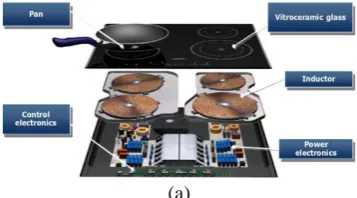
Induction heating appliances are widely used due to advancement in power electronics and digital control. It is most highly preferred due to its high performance, efficiency, power control, safety and cleanness [1]. The general architecture consists of the user interface terminal, power converter topology, and digital control system as depicted in Figure (1). The user interface allows the user to provide the target power delivered to the load. The power converter unit, in which the ac mains voltage is rectified and filtered, provides a dc voltage. An inverter, supplies a variable current of 15 to 40 kHz frequency to the induction coil. This alternating current gives a magnetic field alternating in nature, which produces eddy current and magnetic hysteresis heating up the induction heating pan. Thus the power converter unit delivers the main target power to the induction load. The inverter is the most essential subsystem of the induction heating appliances.
(b)
Figure 1: Induction Heating Appliance (a) General Architecture (b) Power Conversion Scheme
RELATED WORK:
Many different topologies have been proposed for implementing the subsystem like the series resonant half-bridge inverter [2], full-bridge [3], and single-switch resonant inverter [4]. Among these choices the full-bridge topology is proposed in this work. The choice of the proposal is based on the balance between cost, operating efficiency and performance. Normally in domestic induction appliances the system allows the user to select the desired target output power by means of an interface terminal as shown in Figure (2).
Figure 2: Block Diagram of Induction Heating Appliance
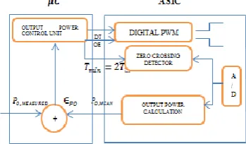
The target power can be adjusted in the range of 100 W to 3.3 kW. In the domestic appliances, an accurate and smooth power control is necessary according to the user needs. Moreover, the heat appliances should operate in a wide operating range. Modulation schemes play a prior role to the above mentioned strategies. To obtain the target output and better efficiency, the full-bridge inverter topology has been proposed [1]. Space Vector Pulse Width Modulation technique is also proposed in order to reduce the switching loss and harmonics with increased accuracy. The modulation techniques should work under soft switching conditions (i.e.,) zero-voltage switching conditions [6]. To obtain these operating conditions, it is important to know exact information about the induction load. The induction system can be modelled as the series combination of a RL circuit [10]. These values depend upon the material of the pan, frequency of excitation, operating temperature, and pan geometry. The inverter is assured to operate inside the Safe Operation Area (SOA) [9], output power and efficiency. The digital control system is used for the proper power delivering to the load by adapting the modulation factors such as peak value of the output current ( ,peak), root mean square value of output current ( ,rms), peak value of output voltage ( ,peak). These parameters are measured for each half period of the main cycle. The digital control system has control block and measurement block [7]. The control block generates the triggering signals of power MOSFET devices considering user defined target output power. The measurement block calculates the required current values from the reconstructed output current provided by ∑∆ ADC [1]. After that the entire system will be implemented in an ASIC as shown in Figure (3).
Figure 3: Digital Control architecture based on Microcontroller and an ASIC
The FPGA can be used to analyse the induction heating system [10]. The output current is put into digital form using sigma-delta Analog to Digital Converter. The advantages of ADC is shaping of the quantization noise and oversampling to achieve good accuracy, to become a cost-effective and efficient solution [13]. The Induction heating system is a low cost appliance, this work proposes the entire system as a power efficient solution. The voltage and current waveforms are conditioned into proper output current x (t) by using a sigma-delta ADC [11] into 1-bit data stream, which is directly processed to obtain the harmonic impedance at a provided frequency. By using digital
LPF block reconstructs the output current by filtering .
proposed scheme achieves output power variation, which simplifies the control strategy [12]. Power MOSFETs provide fast switching speed and ruggedized device design [7]. Moreover, it is widely preferred for all applications at power dissipation levels to appropriately 50W. This paper is proposed as follows:
Section II details the proposed power MOSFET based inverter. Section III details the proposed modulation technique, mainly focused on the output power control and the converter efficiency. Section IV explains the simulation results. Section V regarding the hardware implementation. Finally, the main conclusions and future work are drawn in Section VI.
II
.
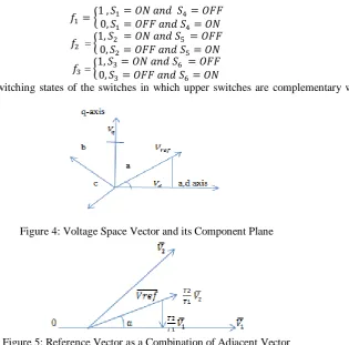
PROPOSED INVERTER TOPOLOGYThe proposed power converter unit is based on the full bridge rectifier which achieves the good balance between cost and performance for the domestic induction heating appliances. In the proposed method, the IGBT have been replaced by Power MOSFETS [5]. The power MOSFETs main characteristics allow the increased efficiency and output power control [10]. In contrast to PWM as triggering to the MOSFET, SVPWM method provides three modulating signals as a single unit called the reference voltage and its component plane is cited in Figure (4). This reference voltage refers 3 variable signals; the switching functions can be given as
{
= {
= {
where are the switching states of the switches in which upper switches are complementary with lower as
shown in Figure (5).
Figure 4: Voltage Space Vector and its Component Plane
Figure 5: Reference Vector as a Combination of Adjacent Vector
The summarization of an algorithm is given as follows:
STEP1: The first step is to find out , and angle (α) by using the following equations which use abs to park
transformation [15].
STEP 2: To Compute the time duration for the corresponding vector . To calculate the switching time duration the following equations are applied:
√ | ̅̅̅̅̅| ( ) (1)
√ | ̅̅̅̅̅̅̅ |
)
(3)
where n=1 through 6 (that is sector 1 to 6)
COMPARISON OF PWM AND SVPWM:
i. SVPWM has 15%Vdc voltage which means more voltage utilization as compared to PWM. ii. SVPWM uses one reference unit to generate three-phase sine wave.
III.FULL BRIDGE RECTIFIER TOPOLOGY
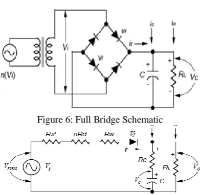
The proposal uses a full bridge rectifier as shown in Figure (6). -forward current through the rectifier diodes,
-Output current -Capacitor current
i,v Small variant time values V, I peak (or) RMS values
Figure 6: Full Bridge Schematic
Figure 7: Equivalent Circuit for Full Bridge Rectifier with Appropriate Values
The transformers turns ratio, n=
where -number of turns in the primary windings as shown in Figure (7). -Number of turns in the secondary windings
-Transformer leakage inductance -Resistance of transformer windings -DC resistance of the secondary winding -DC resistance of the primary winding
(4)
The input voltage is a rectified voltage of the form
| )| (5)
where ω=2Пf, П/ω=t, which is the half-cycle period of the AC input voltage.
Figure8: Full Wave Rectified Sine Wave
)
(8)
At t=0, capacitor will be charged, with a resultant voltage ( ). The rectifier is forward biased until is equal to
or greater than . This point is designated as signifying turn-on and the initiation of rectifier flow which will
increase over time as continues to increase faster than . Thus, the minimum ripple voltage occurs at . As if
begins to flow, that is dependent upon the ratio of and C. This pulse will peak before the incoming voltage does, at
time , at a cut-off angle . is the critical point at which the rectifier current stops and the capacitor continues
providing the entire output current. At , the condition of , the peak voltage proceeds this point by a slight amount and if decreases as drops towards . The resultant current flow through the rectifier and source resistance is not
discharge at a rate that can be computed by using exponential decay at time . If the load draws a constant current the capacitor voltage will linearly decay. The discharge will continue through time until overcomes at a time.
Moreover, does not perfectly tracks if =0 [15].
IV.SIMULATION RESULTS
The proposed technique obtains 230V AC input voltage which is then rectified by the full-bridge topology and inverted by using power MOSFET triggered by using the proposed SVPWM pulses as depicted in Figure (9). The user provided target output power is fed to the control unit. The measurement block computes the values and digital control unit adjusts the power delivering to the load. The system has been designed 1 kW supply to an induction load. The frequency of switching is between 15 kHz to avoid noise. To operate in the appropriate mode the resonant frequency should be lower. The power converter is provided from a supply of 230 V, 50 Hz by means of a full-bridge rectifier. In addition to that, some additional capacitors have been added to obtain a better system. The digital control system general architecture is made up of a microcontroller and an ASIC.
Figure 9: Circuit Diagram of the Proposed System Using Proteus Software
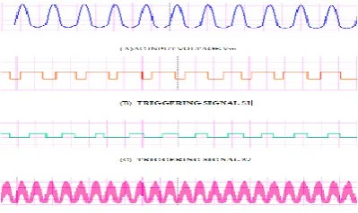
The microcontroller monitors the modulation parameters provided by the user through interface terminal, whereas the ASIC unit generates the triggering signals for the MOSFETs as obtained in Figure (10). In addition to that, the parameter output current ensures the operating mode and achieves the target output power. The proposed technique behaves as expected, verifying the results.
Figure 10: (a) Ac Input Voltage ( )(b) Triggering Signal for MOSFET S1. (c) Triggering Signal for MOSFET S2. (d) Output Voltage ( )
The simulation results of the proposed method are shown in Figure (10). (a) shows the AC input voltage 230 V with frequency=50 Hz. (b) Triggering Signal for MOSFET with voltage=3.5 V with frequency=50Hz. (c)
Triggering signal forMOSFET voltage=3.5 Vfrequency=50 Hz. (d) AC outputvoltage with frequency=50 Hz.
V.HARDWARE IMPLEMENTATION
Figure 11: Implementation of full bridge topology
The above Figure 11 shows the snapshot of the hardware module part of full bridge rectifier.
Powerful IGBT module (half bridge IGBT) is proposed to compute the resonance frequency in the tank circuit to generate a high frequency AC input; hence high frequency response power device as an inverter is needed. 2MBI 50N-120 FUJI IGBT Module, manufactured by collmer semiconductor is used that withstand operating continuous current up to 50A, pulsating current up to 100 A, the operating voltage up to 1200V. Moreover these modules have many features such over-current limiting and built in freewheeling diodes is shown in Figure 12.
Figure 12: Implementation of IGBT
The insulated gate bipolar transistor (IGBT) is used to combine the best features of the bipolar junction transistor and the MOSFET technologies. IGBT device has good forward blocking but limited reverse blocking. The IGBT has 3 terminals. The terminals are called the Emitter (E) and Collector (C), using the BJT terminology, while the control terminals are called the Gate (G), using the MOSFET terminology.
PIC Microcontroller (16F877A) is used to computes the difference of measured and targeted output power delivered to the load.PIC is used here as a pulse generator which is necessary to the input of the IGBT driver. The circuit of microcontroller as shown in Figure (13).
Figure 13: Circuit diagram of PIC Microcontroller
An IGBT inverter frequency generator on each IGBT Gate is needed. PIC microcontroller is used to generate such needed frequencies, but the problem in PIC output signal is its maximum output is 5V which is very low to drive a power IGBT that need gate voltages in range (10-20) V. The general purpose opto couplers consist of a gallium arsenide infrared emitting diode driving a silicon phototransistor in a 6-pin dual in-line. The opto-coupler is used to isolate between high voltage of the inverter and low voltage of the microcontroller where signals and data need to be transferred from one subsystem to another without making a direct ohmic electrical connection. this is because the source and destination are at different voltage levels, like a PIC which is operating on 5Vdc but used to control power inverter which is switching 300Vdc. the link between the two must be an isolated one to protect the PIC from over voltage damage is needed in that situation. Opto-coupler (4N36) for isolating between the half bridge inverter gates and the PWM output from the PIC microcontroller is used.
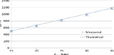
From the hardware implementation the proposed technique behaves as expected, verifying the results. The plot between switching frequencies versus output power is shown in Figure 14 with the ranges between 15 kHz to 35
kHz and the corresponding output power varies from 500 W to 1180W.
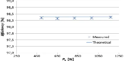
The efficiency plot for the proposed converter is 98.4% for which the output power control varies linearly as shown in Figure 15.
Figure 15: Efficiency Plot for the Proposed Converter Strategy
VI.CONCLUSION
Efficiency is the key concern for an induction heating appliance; hence it reduces the energy consumption and also increases the reliability of the output power. In this paper, a new converter based on the full bridge topology has been presented. This converter uses the power MOSFET in order to allow using a specific modulation technique. This modulation scheme reduces the switching losses and minimizes conduction losses and improves the converter efficiency. Moreover, the output power can be easily controlled by switching frequency, thus avoids the issues in other topologies. Simulation and experimental results confirm that feasibility of the proposed converter and the modulation strategy. As a result, the improved frequency and linear output power control makes this topology very well suited for the domestic induction heating appliance.
REFERENCES
[1] Acero.J, et al., "Domestic induction appliances," IEEE Ind. Appl. Mag.,vol. 16, no. 2, pp. 39-47 Mar./Apr. 2010. [2] Sarnago.H, Lucia, Mediano.A "Class-D/DE dual mode- operation resonant converter for improved-efficiency domestic induction heating system," IEEE Trans. Power Electron., vol. 28, no. 3, pp. 1274-1285 2013.
[3] Chudjuarjeen.S, Sangswang.A, and Koompai.C "An improved LLC resonant inverter for induction-heating applications with asymmetrical control," IEEE Trans. Ind. Electron., vol. 58, no. 7, pp. 2915-2925 June 2011.
[4] Lucia.O, Burdio J.M, Barraging L. A, Carretero C., and Acero "Series resonant multiinverter with Discontinuous-mode control for improved light-load operation," IEEE Trans. Ind. Electron., vol. 58, no. 11, pp. 5163-5171 Nov. 2011. [5] Ha Pham N, Fujita H., Ozaki K., and Uchida N., "Phase angle control of high-frequency resonant currents in a multiple inverter system for zone control induction heating," IEEE Trans. Power Electron., vol. 26, no. 11, pp. 3357-3366 Nov. 2011.
[6] Jimenez O., Lucia O, Barragan L. A., Navarro D, Artigas J. I., and Urriza I.. "FPGA-based test-bench for resonant inverter load” 2013.
[7] Jimenez O., Lucia O., Urriza I., Barragan L. A., Mattavelli P., and Boroyevich D., "FPGA-based gain-scheduled controller for resonant converters applied to induction cooktops," IEEE Transactions on Power Electronics 2013. [8] Egalon J., Caux S., Maussion P., Souley M., and Pateau O. , , "Multiphase system for metal disc induction heating: Modelling and RMS current control," IEEE Transactions on Industry Applications, vol. 48, no. 5, pp. 1692-1699 September/October 2012.
[9] Lucia O., Burdio J. M., Millan I., Acero J., and Puyal D., , "Load-adaptive control algorithm of half-bridge series resonant inverter for domestic induction heating," IEEE Trans. Ind. Electron., vol. 56, no. 8, pp. 3106- 3116 Aug. 2009. [10] Hwang S. H., Liu X., Kim J. M., and Li H., "Distributed digital control of modular-based solid-state transformer using DSP+FPGA," IEEE Trans. Ind. Electron., vol. 60, no. 2, pp. 670-680 , Feb. 2013.
[11] Acero J., Navarro D.Barragan L. A, Garde I., Artigas J. I., and Burdio J. M,., "FPGA-based power measuring for induction heating appliances using sigma-delta A/D conversion," IEEE Trans. Ind. Electron., vol. 54, no. 4, pp. 1843-1852 Aug. 2007.
[12]O. Lucia O., Burdio J. M.,. Barragan L. A, Acer J., and Milan "Series- resonant multiinverter for multiple induction heaters," IEEE Trans. Power Electron., vol. 25, no. 11, pp. 2860-2868 Nov. 2010.
[13] Sung G. M., Yu C. P.,. Hung T. W, and Hsieh H. Y., "Mixed-mode chip implementation of digital space SVPWM with simplified-CPU and 12-bit 2.56 Ms/s switched-current delta-sigma ADC in motor drive," IEEE Trans. Power Electron., vol. 27, no. pp. 916-930 Feb. 2012,.
[14] Ortmanns M. And Gerber’s F. Springer, Continuous-time sigma-delta A/D conversion: Fundamentals, performance limits and robust implementations 2006.