AZAM, FAISAL. AlGaN/GaN MOSHFETs using ALD Dielectrics: A Study in Performance and Reliability. (Under the direction of Dr. Veena Misra).
Gallium Nitride is the most promising semiconductor material for both microwave and power
switching applications. Due to its excellent carrier mobility, high current density, high breakdown
voltage, and high temperature operation AlGaN/GaN devices are extremely attractive for the next
generation of power devices in the 100–650 V range [49]. The increasing demand for more
efficient transistors, higher output power density, higher input impedance, and higher blocking
voltage potential has led to the research and development of GaN over last two decades. Since the
1st demonstration of a GaN high electron mobility transistor (HEMT) in 1993 [8], GaN-based RF
power devices have made substantial progresses including steadily improved growth techniques,
material qualities, enhanced processing technologies, and more optimum device designs. More
recently, advancement of insulating gate and field-management technologies based on the GaN
HEMT structure has resulted in 600 V and above power switching transistors. The trend of the
GaN-based device is towards higher output power density, higher Power-Added-Efficiency (PAE),
higher operation frequencies and improved reliability. In order to achieve these requirements,
novel device designs and processing technologies are being developed.
The greatest impediment for the industry-wide adoption of GaN technology has been, and remains,
achieving a high level of reliability and stability concurrently with high performance operation.
The focus of my research has been to improve upon these weaknesses and provide a forward
momentum for the technology. The devices we worked on were normally-on (depletion-mode),
distributed energy storage devices (DESD), telecom DC-to-DC conversion, and military
applications.
We approached from various technological solutions standpoint to address some of the core
challenges. In particular, we investigated ALD dielectrics and their impact on the gate and access
region of the transistor. The ALD chemistry and effect of oxidants were studied in great detail. We
explored effect of annealing ambient on improving traps. Device design considerations were also
taken into account and optimized such as, dielectric thickness, gate-to-drain separation, etc. We
stressed the devices by making them undergo temperature and bias acceleration tests and followed
a comprehensive characterization suite to evaluate the health of the device. Our efforts
materialized in seeing improvements in several of the performance and reliability metrics. With
the enhancements proven in this work and directions suggested, GaN technology not only provides
more efficacy and solid potential for the near-term applications but also paves the way for energy
© Copyright 2018 by Faisal Azam
by Faisal Azam
A dissertation submitted to the Graduate Faculty of North Carolina State University
in partial fulfillment of the requirements for the degree of
Doctor of Philosophy
Electrical Engineering
Raleigh, North Carolina
2018
APPROVED BY:
_______________________________ _______________________________ Dr. Veena Misra Dr. Mehmet C Ozturk
Committee Chair
ii
DEDICATION
It is to commemorate her unconditional love, affection, and support that I dedicate this dissertation
iii
BIOGRAPHY
Faisal Azam was born in Bangladesh. He received his Bachelor’s degree in Electrical Engineering
from the University of Cincinnati, OH, in 1998 and Masters in Electrical Engineering from
Rensselaer Polytechnic Institute, NY, in 2000.
He joined IBM Microelectronics, Fishkill, NY, in year 2000 as a device characterization engineer
where he worked on bulk silicon and silicon-on-insulator (SOI) technologies optimizing
performance, yield, and reliability objectives. He also played an integrated role in qualifying
advanced CMOS logic and eDRAM products from post tape-out through ramp-up until release to
production.
In year 2007, Faisal joined Samsung Austin Semiconductor, TX, as a process integration device
engineer where he was responsible for test, characterization, qualification and technology transfer
of CMOS logic and flash memory devices.
Faisal returned to school in 2014 and pursued Doctor of Philosophy in Electrical Engineering at
North Carolina State University. He joined the Future Renewable Electric Energy Delivery and
Management (FREEDM) Systems Center as a graduate research assistant under the direction of
Dr. Veena Misra. His research focused on improving performance and reliability of AlGaN/GaN
iv
ACKNOWLEDGMENTS
First, I would like to express my gratitude towards my advisor, Dr. Veena Misra, without whom
earning this Ph.D. would not have been made possible. Her support and guidance throughout this
work were invaluable. Not only does she make an excellent mentor, but she is also a great human
being. A special thanks to my co-advisor, Dr. Bongmook Lee, for countless hours of help. In the
past four years, I learned a lot from him on GaN technology.
Thanks to Dr. Mehmet Ozturk and Dr. Tania Paskova for serving on my committee and providing
critical suggestions.
Thanks to my colleague and friend, Akhilesh Tanneeru, for his feedback and cubicle discussions
throughout the years. I would also like to acknowledge the help and support of my previous and
current group members, Dr. Biplab Sarkar, Dr. Steven Mills, Dr. Michael Lim, and Sizhen Wang.
Thanks to all my friends in Raleigh who have helped me build fond memories during higher
education.
I want to thank the National Science Foundation in earnest for supporting this research through
the FREEDM center. Thanks to Dr. Iqbal Husain for availing funds for the project.
I would also like to thank the cleanroom staff at NCSU Nanoelectronic Fabrication Facility (NNF)
and Shared Materials Instrumentation Facility (SMIF) at Duke University. Thanks to Dr.
Ching-Chang Chung at Analytical Instrumentation Facility (AIF) for training me on the XRD tool and
helping me with crystal phase identification. Thanks to Dr. Jan Genzer for allowing me to use
v Thanks to my mother, Farida Banu, for her unwavering support and compromise. I also want to
thank my sisters, Shireen Chowdhury and Sharmeen Hassan, for their encouragement. Finally,
vi
TABLE OF CONTENTS
LIST OF TABLES ...x
LIST OF FIGURES ... xi
Chapter 1: Introduction ...1
1.1 Review of GaN Technology ...1
1.2 GaN Crystal Structure and Polarization ...5
1.2.1 Spontaneous polarization, PSP ...5
1.2.2 Piezoelectric polarization, PPE ...6
1.2.3 Two-dimensional electron gas (2DEG) ...6
1.3 GaN Transistors ...8
1.3.1 Vertical GaN HEMT ...8
1.3.2 Lateral GaN HEMT ...8
1.4 GaN HEMT Operation Mode ...10
1.5 Key Technological Issues ...11
1.5.1 High gate-leakage current ...11
1.5.2 High electric field ...13
1.5.3 Normally-on transistor ...14
1.5.4 DC/RF dispersion or, current collapse or, dynamic RDS(ON) ...17
1.5.5 Hot electron effect...20
1.5.6 Inverse piezoelectric effect ...21
1.5.7 Post-stress reliability, long-term stability ...23
vii
Chapter 2: Dielectrics, Fabrication Methods, and Experimental Procedures ...26
2.1 Choice of Dielectric Materials ...26
2.1.1 Requirements for the Gate dielectric: ...27
2.1.2 Requirements for the Passivation dielectric:...27
2.1.3 Choice of Candidates for the Gate Oxide and Passivation: ...28
2.2 Atomic Layer Deposition (ALD) ...31
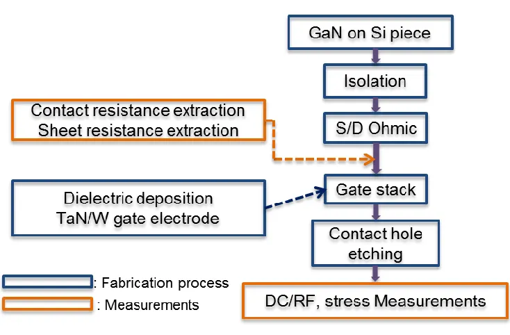
2.3 Transistor Fabrication ...34
2.3.1 Substrate properties ...35
2.3.2 Surface cleaning ...36
2.3.3 HFET fabrication flow ...36
2.3.2 MOSHFET fabrication flow ...38
2.4 Analytical Characterization Methods ...40
2.4.1 Variable Angle Spectroscopic Ellipsometry (VASE) ...40
2.4.2 X-Ray Diffraction (XRD) ...41
2.5 Electrical Characterization Methods ...42
2.5.1 Experimental setup...42
2.5.2 Capacitance-Voltage measurements ...42
2.5.3 Current-Voltage measurements ...43
2.5.4 Pulsed-IV measurements ...43
2.5.5 Reliability tests...45
2.6 Summary ...48
viii
3.1 Introduction ...49
3.2 Experimental Procedures ...51
3.2.1 Device fabrication ...51
3.2.2 Design of experiment ...52
3.3 Physical Characterization of ALD HfO2 Film ...53
3.4 Electrical Characterization of ALD-HfO2 MOSHFET ...54
3.4.1 Capacitance-voltage (CV) characteristics ...54
3.4.2 DC current-voltage (IV) characteristics ...56
3.4.3 Temperature dependence ...59
3.4.4 High temperature reverse bias (HTRB) stress test ...60
3.4.5 DC/RF dispersion / current collapse – gate lag measurement ...61
3.5 Summary ...64
Chapter 4: High Temperature Operation of GaN-on-Si MOSHFETs with ALD Hafnium Oxide (HfO2) ...66
4.1 Introduction ...66
4.2 Output Characteristics as a Function of LGD, T, TOX ...67
4.3 Transfer Characteristics as a Function of LGD, T, TOX ...69
4.3.1 Threshold voltage (VTH) variation ...69
4.3.2 Off-state leakage variation ...71
4.3.3 Peak transconductance (gm,max) variation ...71
4.4 Hysteresis as a Function of LGD, T, TOX ...72
4.5 Drain leakage as a Function of LGD, T, TOX ...73
ix
4.6.1 Dielectric breakdown ...75
4.7 Summary ...76
Chapter 5: Annealing Ambient Effect on GaN MOSHFETs with ALD HfO2 Dielectric ...77
5.1 Introduction ...77
5.2 Experimental Procedure ...78
5.3 Physical Characterization of ALD HfO2 Film ...79
5.4 Electrical Characterization of MOSHFETs ...80
5.4.1 Capacitance-voltage (CV) characteristics ...80
5.4.2 DC current-voltage (IV) characteristics ...82
5.4.3 Temperature dependence ...84
5.4.4 Current collapse – gate lag measurement ...86
5.4.5 High temperature reverse bias (HTRB) stress test ...87
5.5 Electrical Characterization of MOSHFETs with H2O Oxidant ...87
5.6 Summary ...89
Chapter 6: Conclusions and Future Work ...91
6.1 Conclusions ...91
6.2 Future Work ...96
x
LIST OF TABLES
Table 1.1 Comparison of material parameters of Si, SiC and GaN ...3
Table 2.1 Summary of the physical parameters of various dielectrics relative to GaN ...28
Table 2.2 ALD deposition conditions used for different dielectrics ...33
Table 2.3 Epi-layer structure of the vendor substrate ...35
Table 3.1 Device fabrication process summary ...52
xi
LIST OF FIGURES
Figure 1.1 Power electronics market expectation by Yole Développement ...1
Figure 1.2 Theoretical on-resistance vs. blocking voltage capability for Si, SiC, and GaN
based power devices. ...2
Figure 1.3 Prospects of wide bandgap semiconductor transistors. ...4
Figure 1.4 The Wurtzite geometric structure of GaN Crystal (a) Ga-faced and (b) N-faced. ...5
Figure 1.5 Animation depicting AlGaN stretching outward when brought into contact with
GaN. ...6
Figure 1.6 (a) Net positive charge at the AlGaN/GaN interface caused by the sum of
spontaneous and piezoelectric polarization and (b) 2DEG formation and
corresponding conduction band energy profile. ...7
Figure 1.7 (a) Vertical FET and (b) Vertical GaN-on-GaN normally-off JFET. ...8
Figure 1.8 Cross-section of a lateral GaN HEMT (not drawn to scale). ...9
Figure 1.9 GaN HEMT operation modes, starting with the top left going in a clockwise
direction: zero bias, on-state, off-state, and blocking mode. ...11
Figure 1.10 Cross section of a lateral GaN HFET with gate dielectric (MOSHFET structure). .12
Figure 1.11 Cross section of a lateral GaN MOSHFET with gate-connected and
source-connected field plates. ...14
Figure 1.12 Schematic cross section of common normally-off technological solutions. ...16
Figure 1.13 Cascode hybrid E-mode structure. ...17
Figure 1.14 (a) Schematic cross-section of a GaN device showing mechanism of RDS(ON)
increase and (b) dispersion between the large signal AC and DC HEMT
xii Figure 1.15 Hot electron tunneling into the passivation layer under high stress condition. ...21
Figure 1.16 IGS degradation mechanism for reverse bias stress. Crystallographic defects
produced by the inverse piezoelectric effect provide a leakage path across the
AlGaN barrier. ...22
Figure 2.1 Objective of dielectric on AlGaN/GaN in the gate and passivation regions. ...26
Figure 2.2 ALD Pulse sequence and the process for deposition of Al2O3 using TMA and
H2O. ...34
Figure 2.3 Simple schematic of the AlGaN/GaN substrates procured from vendor, as listed
in Table 2.1. ...35
Figure 2.4 Lateral HFET fabrication process and measurement flow. ...37
Figure 2.5 Simple schematic showing the HFET fabrication flow and topography of the
fabricated line device. LG = gate length, WG = gate width, LGS = gate-source
spacing, LGD = gate-drain spacing. ...38
Figure 2.6 Lateral MOSHFET fabrication process and measurement flow. ...39
Figure 2.7 Simple schematic showing the MOSHFET fabrication flow. ...39
Figure 2.8 Simple schematic of the custom built pulsed-IV setup with an oscilloscope and
a pulse generator. Also shown is the custom designed software graphical user
interface on a PC to control the instruments and acquire the transient current
response...45
Figure 3.1 Schematic cross-sectional view of the fabricated AlGaN/GaN MOSHFET. ...52
Figure 3.2 Split table and animation showing examples of single-pulse and double-pulse
xiii Figure 3.3 Comparison of the XRD spectra for ALD HfO2 using H2O oxidant, O3 oxidant,
and JCPDS reference. ...54
Figure 3.4 CV characteristics of oxidant splits (a) H2O incorporation either as a single-pulse
oxidant or as the first oxidant in a series of double-pulse splits, and (b) O3
incorporation either as a single-pulse oxidant or as the first oxidant in a series of
double-pulse splits. ...56
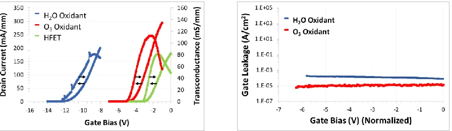
Figure 3.5 Comparison of two oxidants for (a) output characteristics (IDS–VDS), and (b)
extracted specific on-resistance of the AlGaN/GaN MOSHFETs. ...57
Figure 3.6 Comparison of the transfer characteristics for AlGaN/GaN MOSHFETs using
H2O oxidant, O3 oxidant, and an unpassivated HFET. ...58
Figure 3.7 Comparison of the MOSHFET gate leakage between two oxidants. ...58
Figure 3.8 Comparison of two oxidants for (a) static RON variation, (b) VTH variation, (c)
peak transconductance variation, (d) gate leakage variation, and (e) drain leakage
variation of the AlGaN/GaN MOSHFETs as a function of temperature. ...59
Figure 3.9 (a) A typical transfer and transconductance curves during HTRB stress, and (b) comparison of the MOSHFET ΔVTH as a function of HTRB stress time between
the two oxidant groups. ...60
Figure 3.10 Hardware test configuration to measure current collapse. Graph on the right
shows example gate pulse with a sharp rise time and drain current response
recovering to steady state value. ...62
Figure 3.11 DC/RF dispersion: gate lag at (a) room temperature, and (b) elevated
xiv Figure 3.12 Illustration of the ALD physical chemistry and the oxygen molecules
terminating hydrogen and OH– bonds...64 Figure 4.1 Output characteristics of (a) HFET and (b) 20nm ALD HfO2 MOSHFET, as a
function of temperature (LGD = 15 μm). ...68
Figure 4.2 Extracted static Ron,sp of HFET and MOSHFETs plotted as a function of (a) LGD,
at room temperature and (b) substrate temperature at LGD = 15 μm. ...69
Figure 4.3 Threshold voltage (VTH) of HFET and MOSHFETs plotted as a function of (a)
LGD, at room temperature and (b) substrate temperature at LGD = 15 μm. ...70
Figure 4.4 IDS-VGS (linear-mode) of (a) HFET and (b) 20nm ALD HfO2 MOSHFET, as a
function of temperature (LGD = 15 μm). ...70
Figure 4.5 Logarithmic plot of IDS-VGS (linear-mode) showing off-state leakage (a) HFET
and (b) 20nm ALD HfO2 MOSHFET, as a function of temperature (LGD = 15
μm). ...71
Figure 4.6 Peak transconductance of HFET and MOSHFETs plotted as a function of (a)
LGD, at room temperature and (b) substrate temperature at LGD = 15 μm. ...72
Figure 4.7 Hysteresis of HFET and MOSHFETs plotted as a function of (a) LGD, at room
temperature and (b) substrate temperature at LGD = 15 μm. ...73
Figure 4.8 Drain leakage of HFET and MOSHFETs plotted as a function of (a) LGD, at room
temperature and (b) substrate temperature at LGD = 15 μm. ...74
Figure 4.9 Gate leakage of HFET and MOSHFETs plotted as a function of (a) LGD, at room
temperature and (b) substrate temperature at LGD = 15 μm. ...75
Figure 4.10 MOSHFETs with thin insulators showing breakdown with temperature stress
xv Figure 5.1 Comparison of the XRD spectra for ALD HfO2 annealed in N2, FG, and JCPDS
reference. ...80
Figure 5.2 Capacitance-voltage curves of MOS capacitors for HfO2 dielectric annealed in
different ambient, measured at room temperature (a) 10 kHz, (b) 100 kHz, and
(c) 1 MHz. ...81
Figure 5.3 DC current-voltage characteristics of HfO2 MOSHFETs annealed in different
ambient, measured at room temperature, plotted as a function of LGD (a)
extracted static Ron,sp, (b) VTH, (c) peak gm, (d) hysteresis, (e) drain leakage, and
(f) gate leakage. ...83
Figure 5.4 DC current-voltage characteristics of HfO2 MOSHFETs annealed in different
ambient, measured at a constant LGD = 20 μm, plotted as a function of
temperature (a) extracted static Ron,sp, (b) VTH, (c) peak gm, (d) hysteresis, (e)
drain leakage, and (f) gate leakage. ...85
Figure 5.5 DC/RF dispersion: gate lag of HfO2 MOSHFETs annealed in different ambient,
measured at (a) room temperature, and (b) elevated temperature, 150 °C. ...86
Figure 5.6 Comparison of the MOSHFET ΔVTH as a function of HTRB stress time between
the two annealing ambient. ...87
Figure 5.7 Capacitance-voltage curves for H2O oxidant-based HfO2 dielectric, annealed in
different ambient, measured at room temperature (a) 10 kHz, (b) 100 kHz, and
(c) 1 MHz. ...88
Figure 5.8 Comparison of ΔVTH as a function of HTRB stress time between the two
1
CHAPTER 1: Introduction
1.1
Review of GaN Technology
More than half the electricity produced in the USA is one way or another controlled by power
semiconductor devices. Qorvo projects that by 2030, as much as 80 percent of the electricity
generated will pass through one or more power conversion stages from generation to consumption
(a 30 percent increase from today) [1]. This directly translates to a high demand for switching
devices. According to Yole Développement, the market for power electronics approaches $18
billion by year 2020 (Figure 1.1) [2]. That’s a large industry and there is a lot of competition to
provide high performance products at a low cost. The basic requirements for semiconductors used
in power conversion are efficiency, reliability, controllability, and cost effectiveness. Without
these attributes, a new device structure would not be economically viable.
2 Silicon is still dominating as a power semiconductor device. However, it is rapidly approaching
theoretical limitation making it difficult for further efficiency [1]. There have been efforts to push
beyond limits of Si by novel device structures such as, insulated-gate bipolar transistor (IGBT)
and superjunction (SJ) MOSFETs [3]. Yet there is an increasing need for devices with higher
blocking voltage capacity to be used in domestic appliances, motor drives, hybrid and electric
vehicles, railway, and very high power capacity energy transmission. The tradeoff between two
most fundamental parameters, specific on-state resistance (Ron) and off-state breakdown voltage
(BV), is critical for power switching applications. Figure 1.2 shows the theoretical limitation of
these metrics for Si, SiC and GaN devices [4]. For a given voltage rating, Ron of GaN based devices
is nearly three orders of magnitude lower than that of Si and it also surpasses the limit of SiC,
indicating its great potential in high voltage and high power density applications.
3 Ron and BV are related by the equation (1.1) [5] where the denominator, commonly known as Baliga’s Figure of Merit (BFOM), is a strong indicator for how suitable a material is for power
switching applications.
(1.1)
where BV is the breakdown voltage, μ is the mobility, is the dielectric constant, and Ec is the
critical electric field for breakdown.
Table 1.1 also compares various figures of merit of the three semiconductors [6]. The Baliga's
Figure of Merit (BFOM) represents the on-state resistive loss, and Baliga’s high-frequency figure
of merit (BHFFOM) represents switching loss. In Table 1.1, these figures of merit have been
normalized to Si performance and are shown for comparison. GaN devices outperform existing Si
and SiC devices for most power conversion applications except at extremely high temperatures
where SiC trumps all other materials [1].
Table 1.1: Comparison of material parameters of Si, SiC and GaN [6].
4 It’s the wide bandgap (3.4 eV) that allows GaN to have high critical field (> 3x10⁶ V/cm) and
stability at high temperatures [10]. GaN having 10 times higher breakdown strength compared to
Si means that 10 times the operating voltage can be applied to GaN devices compared to Si devices
for a given device dimension. Additionally, the ability to form a high density two-dimensional
electron gas (2DEG) in the GaN near the AlGaN/GaN heterointerface by polarization doping
allows for very high electron mobility (μn) while maintaining a high sheet charge density (ns) in
the drift region [14]. This means lower specific on-state resistance Ron which further scales with
the length of the device drift region necessary to maintain a given breakdown voltage. The more
compact GaN devices feature much lower Ron compared to Si devices. Thus, GaN devices enable
high breakdown voltages and high current levels simultaneously and feature small semiconductor
areas. This essentially translates to high switching frequencies at high power levels. Figure 1.3
shows prospects of wide bandgap (WBG) semiconductor transistors in the power,
high-frequency domain for near-term applications [7].
5
1.2
GaN Crystal Structure and Polarization
GaN can exist in either a cubic crystal structure (zinc blende phase) or a hexagonal (Wurtzite)
crystal structure [10], [66], the latter being chemically stable and mechanically robust. The polar
hexagonal crystal structure is of most technological interest. More specifically, GaN-based
materials has two types of polarization that makes the structure distinctive [14].
1.2.1
Spontaneous polarization, P
SP:
This is intrinsic property of the material. There is a strong polar bond between Ga and N atoms.
The polarity could be either Ga-faced or N-faced, as shown in Figure 1.4. Currently all
high--quality material is grown with Ga polarity in the [0001] direction (c-axis) [11]. The polarization is
described by equation (1.2) [14].
(1.2)
(a) (b)
6
1.2.2
Piezoelectric polarization, P
PE:
This results from mechanical strain between AlGaN/GaN heterojunction layers. When AlGaN is
grown on top of GaN, due to lattice mismatch (2.4% difference between AlN and GaN at room
temperature [66]), AlGaN biaxially stretches outward causing a tensile strain [117], [126]. This is
illustrated in Figure 1.5. The polarization is described by equation (1.3) [14].
(1.3)
where a is the lattice constant of the strained layer, a0 is the length of GaN hexagonal edge, e31 and
e33 are the piezoelectric coefficients, and C13 and C33 are elastic constants.
Figure 1.5: Animation depicting AlGaN stretching outward when brought into contact with GaN.
1.2.3
Two-dimensional electron gas (2DEG):
The two polarizations added together results in a net positive charge at the AlxGa1-xN/GaN
heterointerface as shown in Figure 1.6(a) [11]. Simultaneously, electrons are attracted at the
7 and form 2DEG under the AlGaN barrier. This is shown in Figure 1.6(b). The total polarization
charge is given by equation (1.4) [14],
(1.4)
(a) (b)
Figure 1.6: (a) Net positive charge at the AlGaN/GaN interface caused by the sum of spontaneous and piezoelectric polarization [11] and (b) 2DEG formation and corresponding conduction band energy profile [95].
The disparate polarization-induced 2DEG effectively reduces on-resistance and thus power loss.
A typical sheet carrier density (ns) of 1013 cm-2 and electron mobility of 2000 cm2/V-s have been
reported in the 2DEG [9], [14]. The consequential high concentration of electrons with very high
mobility makes AlGaN/GaN heterostructure a high electron mobility transistor (HEMT).
Confinement of the 2DEG close to the interface and ns are sensitive to different physical properties
such as, AlGaN composition, polarity, strain, barrier thickness, etc. Brown et al. [90] has cited, for
8
1.3
GaN Transistors
1.3.1
Vertical GaN FET:
Usually, the choice for a high power device is a vertical drift region. The Ron is much lower. Also,
since the high electrical field of the active area does not reach the surface, BV achieved can be
much higher (> 1200V) [124]. Additionally, the vertical architecture virtually eliminates current
collapse, while enhancing switching speeds and thermal handling capabilities [1]. However, the
vertical devices necessitate high quality, thick epitaxial layers, and conductive substrates as well
as a conductive interface [124]; i.e., a homo-epitaxy on expensive bulk GaN. Hence, lateral FET
is a more pragmatic solution.
(a) (b)
Figure 1.7: (a) Vertical FET [124] and (b) Vertical GaN-on-GaN normally-off JFET [50].
1.3.2
Lateral GaN HEMT:
Most of the GaN devices available today are lateral heterojunction field-effect transistors (HFETs),
also known as high electron mobility transistors (HEMTs) [50]. Figure 1.8 shows cross-section of
9 effective option. The AlGaN/GaN structure creates 2DEG with a high sheet carrier density (1x10¹³
cm-2) and a high electron mobility (2000 cm2/V-s) [9] which effectively produces a low specific on-resistance. However, because of the native 2DEG channel, the HFET is inherently a
depletion-mode (normally-on) device. Another weakness of the HEMT structure is high gate leakage. Also,
AlGaN surface states and traps in the access regions increase the dynamic on-state resistance [50].
Figure 1.8: Cross-section of a lateral GaN HEMT (not drawn to scale).
For lateral GaN HEMTs with GaN-on-silicon epiwafers, operating voltages are typically limited
to 650 V or less [1]. For higher voltage applications, switching from silicon to SiC substrates
overcomes this limitation. However, other than the increased cost due to expensive substrate, the
lateral device size also needs to be increased to support higher voltages. In which case, superior
10
1.4
GaN HEMT Operation Mode
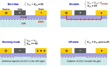
Zero bias: When gate bias (VGS) = drain bias (VDS) = 0V, with the 2DEG present.
On-state: When VDS applied, current starts to flow between source and drain. The exact
mechanism of conduction through the AlGaN layer is unknown. However, after annealing, a strong
structural changes occur in the Ti/Al/Ni/Au metal stack, and a Schottky to ohmic transition is
observed in the temperature range of 600–800 °C. Commonly, it is assumed that the formation of
a TiN metallic compound during annealing, driven by the outdiffusion of nitrogen atoms from
GaN, leaves behind high concentration of nitrogen vacancies below the interface, causing the GaN
to be heavily doped n-type [115], [128]–[130]. Thus favoring the tunneling process of electrons
through the AlGaN barrier and ohmic contact formation.
Off-state: A sufficiently negative VGS needs to be applied to the gate to deplete the 2DEG
underneath. This condition is also referred to as pinch-off.
Blocking mode: This is a more realistic situation when devices are used in power switching applications. The biasing condition is similar to off-state with a much higher bias applied to the
drain. This forms a virtual gate which causes additional depletion of 2DEG in the drift region. The
11
Figure 1.9: GaN HEMT operation modes, starting with the top left going in a clockwise direction: zero bias, on-state, off-state, and blocking mode.
1.5
Key Technological Issues
In spite of the great potential of GaN-on-Si high voltage transistors, its application to power
electronics is currently limited by important challenges. The major issues are discussed below.
1.5.1
High gate-leakage current
A conventional heterojunction-field-effect transistor (HFET) device with Schottky gate suffers
large gate-leakage current that limits device performance. The leakage gets worse as temperature
is elevated. In particular, the gate leakage deteriorates the transistor characteristics by increasing
the subthreshold current and shunting the gate to channel capacitance [39]. Both these factors
12 until time-dependent dielectric breakdown (TDDB) occurs. Hence, a reduction in gate leakage can
potentially delay TDDB and improve life.
Using a metal-oxide-semiconductor HFET (MOSHFET) structure with gate dielectric is a very
effective way to reduce gate-leakage current [13]. The gate metal is isolated from the AlGaN
barrier layer by a dielectric film such as SiO2, Al2O3, HfO2, and so forth, as seen in Figure 1.10.
Hence, the MOSHFET gate behaves more like a MOS gate structure rather than a Schottky barrier
gate in regular HFETs.
Figure 1.10: Cross section of a lateral GaN HFET with gate dielectric (MOSHFET structure).
A properly designed AlGaN barrier layer is fully depleted by electron transfer to the adjacent GaN
layer. Therefore, the gate insulator in the MOSHFET couples with the AlGaN epilayer, ensuring
very low gate-leakage current and allows for a large negative to positive gate voltage swing [88].
Data shows MOSHFET gate-leakage current can be up to six orders of magnitude smaller than for
13
1.5.2
High electric field
In the off-state and blocking mode, there is a high electric field near the gate edge on the drain
side, due to the sharp edges of a rectangular gate. This could generate high energy carriers (hot
electrons) that can be trapped in the passivation layer, AlGaN barrier layer, or in the interface
between these layers. They could widen the surface depletion region thereby leading to
degradation in DC and RF performance. Also, high electric field can cause gate breakdown that
can be attributed to the generation of defects induced by the electric field; when the density of
these defects becomes sufficiently high, a percolative conductive path is formed, and gate leakage
current sharply increases [49].
Device design improvements (Figure 1.11) comprising gate and source-connected field plates are
an effective way to reduce the electric field [116], thereby reducing trapping effect and increasing
breakdown voltages [12], [13]. This further suppresses the increase in on-state resistance as well
as gate leakage degradation. Generally, the longer the field plate, the more output power can be
achieved. However, the capacitance between connected field plate and drain becomes
gate-to-drain capacitance that can lower switching frequencies [13]. Also, the source-connected field
14
Figure 1.11: Cross section of a lateral GaN MOSHFET with gate-connected and source-connected field plates.
1.5.3
Normally-on transistor
For power switching applications, normally-off operation with the threshold voltage above 3V is
strongly required in order to prevent the mis-operation caused by noises [12], [90], [91]. GaN
inadvertently conducts electrical current. The 2DEG in a HEMT device requires a negative gate
bias to turn off the conduction current, thus, presenting the conventional AlGaN/GaN HEMT
devices as normally-on or depletion-mode devices. If the gate fails current will continue to flow.
Normally-off devices or enhancement-mode (E-mode) AlGaN/GaN HEMTs can greatly simplify
circuit designs, improve system reliability, and provide fail-safe operation [90]. Various
techniques have been developed to achieve an E-mode device. The common solutions are:
(a) Recessed Schottky gate [12] – For thick AlGaN layers, Fermi level is pinned by the surface donors. This creates the 2DEG. If the barrier underneath the gate is reduced to a thickness of a
few nanometer (typically 3–5 nm) [116], no polarization induced 2DEG can be formed. Gate
15 these devices may be critical, since the gate is separated from the channel only by a few
nanometer. This leads to large electrical fields at the drain side edge of the gate unless other
precautions are taken [116]. Recessed-gate technique can be used to modulate VTH, however
it may come at the cost of performance degradation and non-uniformity [90], [100].
(b)p-GaN gate [50] – The placement of localized negative charges underneath the gate metal shifts the conduction band of the channel region above the Fermi level and thus creates
normally-off behavior. Essentially, channel is depleted by the high built-in potential of the
P-N junction. Persistent negative charges can be introduced by p-type doped GaP-N or AlGaP-N
layers [116]. Using this structure the threshold voltage value obtained is usually low, around
1V [90], [124].
(c) Fluorine-based plasma treatment [94] – The negatively charged fluorine ion incorporation by implantation into the AlGaN barrier layer. The charge drives away the 2DEG and shifts the
gate-threshold voltage to slightly above 0V with the maximum gate voltage around 1V [124].
Reliability issues may arise since F– incorporation is not stable at high electric fields unless special precautions are taken [116]. While Fluorine plasma treatment was introduced to
provide negative charge, it may affect device uniformity and stability [90], [100].
(d)Inversion-type E-mode MISHFET [93] – The AlGaN barrier layer is completely removed, hence no 2DEG, in the gate region. The gate is placed directly on top of the GaN channel layer
and separated by a suitable gate insulator such as, SiO2, Si3N4, Al2O3 [116]. Therefore, if the
gate is forward biased, an inversion layer is formed under the isolator leading to a current flow.
16 (e.g., inverse piezoelectric effect [112]) may be reduced in this case. However, since this
approach requires a recess, uniformity is questionable.
Figure 1.12: Schematic cross section of common normally-off technological solutions [116].
An alternative solution is a cascode hybrid E-mode structure shown in Figure 1.13 [52], which is
currently the most commercially viable solution [48]. In this configuration, the source of the
high-voltage AlGaN/GaN HEMT is connected to the drain of the low-high-voltage Si power MOSFET and
the gate of the high-voltage HEMT is connected to the source of the Si power MOSFET which
serves as the ground or reference terminal. The device can be controlled by biasing the gate of the
Si power MOSFET while the drain of the GaN HEMT is connected to the load and the output
17
Figure 1.13: Cascode hybrid E-mode structure [52].
In this circuit, the Si MOSFET is turned on with a positive voltage on the gate. When the depletion-mode GaN transistor’s gate voltage goes to near-zero volts, it turns on. Current can now pass
through the depletion-mode GaN HEMT and the MOSFET, which is connected in series with the
GaN HEMT. When the voltage on the MOS gate is removed, a negative voltage is created between
the depletion-mode GaN transistor gate and its source electrode, turning the GaN device off. The
drawbacks of cascode circuit configuration are switching speed limitation [50], larger area, power
loss due to more transistors, and a max operating temperature of 150 °C due to silicon junction
[96]. Cascode configuration is practical for larger than 200 V rating [10]. At such high voltage
rating the low voltage MOSFET does not add significantly to the on-resistance of the cascode
circuit.
1.5.4
DC/RF dispersion or, current collapse or, dynamic R
DS(ON)Current collapse is a phenomenon whereby the drain current decreases as a result of electron
trapping into the AlGaN surface states [11]. This is perhaps the most critical reliability concern.
The main cause of dispersion effects originates from the presence of trap centers related to surface,
bulk, and interface states [13]. These trapping states are assumed to be associated with surface
18 absorbed from the ambient environment [26]. In the off-state, electrons from the gate are injected
into the empty surface donors required to maintain a 2DEG. These surface states, when filled with
electrons, create a layer of charge at or near the surface that act as a virtual gate and deplete the
2DEG in the high field region between the gate and drain. Figure 1.14(a) depicts the mechanism
of RDS(ON) increase and Figure 1.14(b) shows simulated graphical effect. In the on-state, under AC
drive, the electrons contained in the surface layer get detrapped; however, cannot fully modulate
the channel charge due to long-time constant of the donor traps that range from seconds to
microseconds [26]. This results in a reduced channel current and higher on-resistance (symptoms
of dispersion), and an increase in knee voltage [104].
The mechanism is understood as a transient and recoverable reduction in drain current response; a
finite time required by the surface traps to respond to an external voltage step. Similar degradation
is also observed via threshold voltage shift, gate-lag and drain-lag transients. This increases
on-resistance and therefore, limits device performance. Although transient, this effect can cause the
device to excessively self-heat and fail prematurely [67]. Furthermore, electrons can be trapped in
the AlGaN barrier layer itself or in the GaN buffer layer below. Hence, the trap density can increase
as the device ages, making the dynamic RDS(ON) effect worse. The effect is compounded at elevated
temperatures [25]. The high energy electrons can generate traps, further promoting charge
trapping. There are also reports that claim the dispersion effects may be irreversible if certain
critical electrical fields are exceeded [116].
The magnitude of current collapse is strongly dependent on the electric field at the gate-edge where
electrons can be accelerated [53]. Surface passivation, or surface treatments, can be effective at
19
(a) (b)
Figure 1.14: (a) Schematic cross-section of a GaN device showing mechanism of RDS(ON) increase [67] and (b)
dispersion between the large signal AC and DC HEMT characteristics simulated by a 80 μs pulse on the gate [11].
Passivation of AlGaN surface by using different dielectrics has been found to eliminate the
dispersion effect. For instance, SiN passivation has been shown to be more effective than SiO2,
HfO2, and Al2O3 passivated devices at minimizing traps and reducing current collapse [27], [106].
If used in the gate region however, the higher dielectric permittivity of Si3N4 (7.5) vs. SiO2 (3.9)
causes threshold voltage (VTH) increase to be higher.
Device design improvements using gate and source field plates are an effective way to reduce the
electric field thereby suppressing the increase in on-state resistance. Surface passivation, or surface
treatments, can also be effective at reducing the surface trap density and thereby reducing
hot-electron degradation. The use of a conducting substrate acting as a backside field plate helps to
mitigate electron trapping in the buffer region beneath the channel [53]. It was reported that
dynamic RDS(ON) was much improved with GaN devices built on conductive silicon substrates
compared to GaN devices built on non-conductive sapphire substrates. In addition, better
confinement of electrons in the potential well and overall improvement in the material quality of
20 One of the technological solutions that have been proposed as a possible cure for this detrimental
effect consists of using GaN/AlGaN/GaN epitaxial structures with a thin (typically 3–5 nm)
n-type-doped GaN cap layer. It has been suggested to act as a “surface-charge-control” layer that
reduces the effect of surface polarization charge [108], [119], [120]. However, Meneghesso et al.
disputes such claim being concrete [105]. Degradation under RF drive has also been correlated to
different epi structures comprising the AlGaN/GaN HFET. For example, reducing the AlGaN
barrier thickness significantly improved device reliability. This improvement is attributed to a
more stable material structure with less lattice strain in the AlGaN barrier layer.
1.5.5
Hot electron effect
A permanent device degradation after high VDG stress under on-state conditions has been attributed
to the presence of hot electrons [126]. In a GaN HEMT device where extremely high electric field
may be present, electrons can gain sufficient high energy to escape the channel and get trapped in
the AlGaN layer under the gate, or in the gate-drain region where the electric field is maximum,
either at the surface or within the passivation layer, or in buffer traps [125] [127]. This is illustrated
by Figure 1.15. These “hot electrons” may form the so called virtual gate [102] and deplete channel
21
Figure 1.15: Hot electron tunneling into the passivation layer under high stress condition [127].
Hot electron effects, with generation of deep levels and trapping of electrons in the dielectrics
or/and at surfaces and interfaces under the gate as over the gate-drain access region may occur
both, during off-state tests or (more frequently) during semi-on and on-state tests [125].
The term "hot electrons" refers to non-equilibrium electrons which acquire kinetic energy values
sufficient to overcome potential energy barriers, be injected into buffer, barrier or insulating layers
and be trapped there, break atomic bound and create interface states or activate traps. According
to the various experimental conditions, material properties and device weaknesses, hot electrons
may give rise both to parametric, gradual, permanent or recoverable positive or negative threshold
voltage shifts and/or to decrease of transconductance [125]. Hot electron effects can be evaluated
by means of electroluminescence microscopy and spectroscopy.
1.5.6
Inverse piezoelectric effect
This degradation is related to strain relaxation theory driven by electric fields [112]. GaN HEMTs
are predicated on the piezoelectric properties of the material in conjunction with spontaneous
22 the lattice mismatch allows high electron channel densities to form at the AlGaN/GaN interface.
Under large reverse gate stress, the high vertical electric fields concentrated at the gate edge on the
drain side can increase the tensile strain in the AlGaN barrier layer due to the inverse piezoelectric
effect. When a critical drain-gate voltage VDG is reached and the mechanical stress becomes
excessive, strain can relax through crystallographic defect formation, such as dislocations [112],
[113], [117], [118]. These defect states not only degrade IDS and RDS by trapping electrons but also
aid trap-assisted electron tunneling between gate and channel through the AlGaN barrier,
effectively lowering the Schottky barrier height of the gate. The effect is illustrated in Figure 1.16.
Figure 1.16: IGS degradation mechanism for reverse bias stress. Crystallographic defects produced by the
inverse piezoelectric effect provide a leakage path across the AlGaN barrier [113].
In order to prevent this mode of IGS degradation, it is necessary to reduce the elastic energy and
the vertical electric field in the AlGaN barrier. Device designs that mitigate the electric field should
also improve the reliability due to this mechanism. Examples are GaN cap, surface passivation,
23
1.5.7
Post-stress reliability, long-term stability
GaN devices have a tendency to show performance degradation post-stress that may be recoverable
or sometimes irrecoverable [114]. Surface charge plays a major role yet the trapping mechanism
is not fully understood. The trapping and detrapping effects may lead to significant device drift,
with change in the threshold voltage and transconductance [118]. Pre-existing deep levels on the
surface, at interfaces, within the GaN buffer, and within the semi-insulating substrate can originate
from threading dislocations, impurities, ligands, and oxide-defects. These can degrade both the
static and dynamic performance, promoting metastable charge-trapping effects, threshold-voltage
instabilities, and on-resistance increase [25]. There may be process-induced instabilities, especially
in connection with compensating species (Fe or C), contaminants like H, F, O, or defects [125].
Also, after device operation, increased trapping behavior has been observed. At the present time,
physical understanding of the fundamental mechanisms behind device degradation is still
insufficient. The "virtual gate" effect proposed by R. Vetury et al. is usually used to explain device
degradation [102].
In MOSHFETs, threshold voltage instabilities and Time Dependent Dielectric Breakdown
(TDDB) depend on the chosen gate dielectric material and on the related deposition techniques
[49]. A high quality gate insulator with a high breakdown voltage is needed. Time dependent
degradation can be induced by trap creation and formation of conductive percolative paths between
gate and channel [125]. Research has focused on reducing or eliminating device drift and leakage
currents under the high field and high power conditions associated with device operation [13].
Techniques include improving material quality (reducing defect density) of both substrates and
epitaxial layers, surface passivation to combat current collapse and suppress gate-leakage current,
24 The group III-nitride semiconductors have been considered an ideal candidate for high temperature
(TCH > 300 °C) electronic devices due to their large band gap and resulting low thermal carrier
generation rate [25], [51]. On the other hand, thermal and self-heating effects are very pronounced
in any power semiconductor device [85]. Lateral devices have poor thermal handling capability
due to the silicon substrate [1]. Degradation in DC characteristics at elevated temperatures has
been reported. Current collapse has been shown to worsen with increasing temperature [25]. The
positive temperature dependent RON increase could represent a serious issue for GaN-based
electronics, which are supposed to be operated in high-temperature conditions. Such switching
characteristics or the transient characteristics at high temperatures have not been well documented.
Moreover, the mechanisms responsible for reliability issues have not yet been fully established
given the complexity of interface states [101]; however, remain a critical concern preventing
widespread adoption of GaN technology. Devices for power switching applications must
demonstrate long-term stability; in particular they should maintain good current blocking
capabilities in the off-state, constant threshold voltage, low static and dynamic on-resistance.
1.6
Project Goals and Thesis Outline
This dissertation focuses on performance and reliability enhancement of normally-on AlGaN/GaN
lateral MOSHFETs for high voltage switching applications. There was considerable focus on the
development of the device process as well as gaining an understanding of device operation and the
25 This chapter (Chapter 1) covers the essential background on GaN-based transistors. Material
properties and merits are reviewed. Device principals and operation modes are outlined. The key
challenges with GaN devices are discussed in details.
Chapter 2 provides an overview on choice of dielectric materials for GaN MOSHFETs along with
ALD technique. Device fabrication and characterization methods are also discussed.
Chapter 3 provides investigation of ALD oxidants. Devices are characterized in DC, large-signal
microwave power, and under stress. Process optimization through use of O3 oxidant provides
improved DC and RF performance along with enhanced reliability compared to water oxidant
based devices.
Chapter 4 presents a systematic study of AlGaN/GaN MOSHFETs as a function of dielectric
thickness, gate-to-drain distance, and temperature. A comprehensive electrical DC
characterization is performed, and an optimal dielectric thickness is recommended.
Chapter 5 presents investigation of high temperature annealing ambient, nitrogen (N2) and forming
gas (FG). Devices are characterized in DC, large-signal microwave power, as a function of
temperature, and under stress.
Chapter 6 concludes with summary of the results obtained and outlook for future work towards
26
CHAPTER 2: Dielectrics, Fabrication Methods, and
Experimental Procedures
2.1
Choice of Dielectric Materials
There has been a lot of research effort for GaN-based metal-oxide-semiconductor (MOS) devices
due to reduced gate leakage, greater voltage swings, higher drain current, higher transconductance,
and better thermal stability compared with the Schottky-gate devices. In addition, dielectric used
as surface passivation minimizes the current collapse that originates from surface traps.
However, finding the most appropriate dielectric materials is challenging and often involves a
compromise of the required properties such as, permittivity, conduction/valence band offsets,
breakdown strength, thermal stability, and interface trap density. A high dielectric constant is
preferred to preserve maximum channel control but a large conduction band offset (CBO) is
favorable to reduce gate leakage currents. Typically, the bandgaps of insulators show inverse
relation to dielectric constants, i.e. the larger the k value, the smaller the bandgap. Figure 2.1 shows
the requirements of dielectrics on AlGaN/GaN in the gate and passivation regions.
27
2.1.1
Requirements for the Gate dielectric:
For any gate insulator candidate being considered, there should be a large dielectric bandgap
leading to sufficient conduction band offset to GaN to ensure a significant barrier height (> 1 eV)
needed for low gate leakage currents [37], [66]. A large CBO prevents tunneling of electrons
through the dielectric and reduces electron trapping which can cause time-dependent dielectric
breakdown [89]. For example, SiO2 on GaN has a large CBO of 2.56 eV [75].
A high dielectric constant is preferred to maximize gate control over the channel and increase
transconductance [98], [107]. Example of high-k dielectrics are Al2O3 (εr = 9.6) and HfO2 (εr = 18.5) [21]. For the depletion-mode HEMT, insertion of a gate insulator shifts device threshold
voltage (VTH) towards the negative direction due to the decreased gate barrier capacitance.
Dielectrics with relatively low-k characteristics, such as, SiO2 and Si3N4 (εr = 3.9 for SiO2 [21] and
7.5 for Si3N4 [66]), cause large negative VTH shifts [107]. A high-k dielectric as the gate oxide
material to replace SiO2 (or Si3N4) not only minimizes VTH shift but also allows the physical
thickness of the oxide to be increased, thereby reducing the gate leakage current, while maintaining
or increasing capacitance per unit area of the gate oxide.
2.1.2
Requirements for the Passivation dielectric:
In the access area the primary objective is to effectively passivate surface states and minimize
interface traps with AlGaN/GaN. The interface states cause various operational stability and
reliability issues in GaN-based MOSHFETs such as threshold voltage instability and current
28
2.1.3
Choice of Candidates for the Gate Oxide and Passivation:
Table 2.1 lists physical parameters of some of the popular dielectrics on AlGaN/GaN. A brief
description of the dielectrics follow.
Table 2.1: Summary of the physical parameters of various dielectrics relative to GaN [21], [66], [75].
Silicon dioxide (SiO2), Silicon nitride (Si3N4)
On AlGaN/GaN, the most extensively researched dielectrics are SiO2 [65] and Si3N4 [64] which
have been considered both as gate insulators and channel passivation layers [101]. Their appeal is
largely related to their current widespread use in Si-based technologies, and thus they are
well-understood materials. Furthermore, they have been proven effective at reducing leakage current
by ~4 orders of magnitude.
The main advantage of SiO2 is its high conduction band offset to GaN (2.56 eV) [75] that makes
it very effective at suppressing gate leakage. On the other hand, Si3N4 has a higher dielectric
constant (7.5) at the expense of the band gap (5.3 eV). Si3N4 is advantageous because it passivates
nitrogen-vacancy related defects on the AlGaN surface during dielectric growth [101]. Ultimately,
this results in a lower Dit and reduced DC/RF dispersion. For example, the Dit of Si3N4/GaN was
found ~6 times lower than the Dit of SiO2/GaN. Therefore, SiO2 has been associated with
displaying poor gate-lag characteristics [22]. On the contrary, while Si3N4 helps to alleviate the
Dielectric Dielectric constant [21], [66]
Energy band gap (eV) [66]
Conduction band offset to GaN (eV) [75]
ALD SiO2 3.9 9.0 2.56
ALD Al2O3 9.6 8.0 1.96
ALD HfO2 18.5 5.8 1.51
ALD HfAlO 14.0 6.4 1.61
29 problem of current collapse, it suffers from large reverse leakage current due to having smaller
conduction band offset to GaN (1.3 eV) [101]. Also, Si3N4 dielectric has been found to deteriorate
breakdown characteristics. [72].
Aluminum oxide (Al2O3)
Amorphous Al2O3 is one of the leading candidates for insulators in GaN-based devices because of
the wide band gap (8 eV), sufficient permittivity (9.6), high breakdown field (10 MV/cm), high
thermal (~ 900 °C) and chemical stability on AlGaN [21], [24], [66], [75], [91]. Al2O3-passivated
AlGaN/GaN exhibits excellent performance in suppressing gate leakage, likely a result of the large
conduction band offset to GaN (1.96 eV), and reducing current collapse due to relatively low
interface state density [21]. However, the dielectric constant of Al2O3 is still relatively low in
comparison with other materials [75], and thus, Al2O3-passivated devices may also be
characterized by large threshold voltage shift and lower transconductance [24], [43]. Ye et al. [24]
reported a midgap interface trap density of 16nm ALD-Al2O3/GaN at the range of 1011–1012 cm−2
eV−1.
Hafnium oxide (HfO2)
Amorphous HfO2 have shown significant promise because of their high permittivity (18.5) and
sufficient band gap (5.8 eV) [21], [23], [65], [66]. For this reason, HfO2 is currently used to replace
SiO2 as the gate insulator in Si-based MOSFET fabrication, which allows for device scaling [43].
Its conduction band offset to GaN is 1.51 eV [75], which could fulfill the prerequisite for good
gate dielectric, which requires a CBO of at least 1 eV to ensure a substantially low gate leakage
30 Transistors with HfO2 exhibited high drain current, low on-resistance, low leakage currents, and
great immunity to current collapse [23], [72]–[74]. The HfO2 passivation is believed to greatly
reduce the surface trap density and improve reliability [74], [75]. Chang et al. [44] reported 14.8
nm thick ALD-HfO2/GaN with a high drain current (IDS, max ~ 230 mA/mm), low gate leakage
current density (10−8 A/cm2), low interfacial density (5−8 x 1011 cm−2 eV−1), and negligible current collapse. Although it is possible to achieve a lower gate leakage with Al2O3 gate oxide (owing to
larger CBO to GaN), HfO2 still provides adequate low gate leakage while resulting in a less
threshold-voltage shift and higher transconductance compared to Al2O3 [43].
The drawback of HfO2 dielectric is that it is less thermally and chemically stable than Al2O3, where
amorphous HfO2 crystallizes into predominantly monoclinic polycrystalline films on Si at only
400 °C [75]. This is disadvantageous as crystalline structures are more likely to contain grain
boundaries, which enhance leakage.
Hafnium aluminum oxide (HfAlO)
Another solution is to use ternary compounds on AlGaN such as HfAlOx [63], HfSiOx [75], or,
use a stack gate structure (e.g., HfO2/Al2O3) [71] to obtain a good trade-off between dielectric
constant and conduction band offset and achieve better chemical and thermal stability. For
example, Yue et al. [71] fabricated a stack gate structure with HfO2/Al2O3-passivated AlGaN/GaN
MOSHFET using ALD. Their device had minimal C-V hysteresis, a small threshold voltage shift,
a maximum drain current of 800 mA/mm, a peak transconductance of 150 mS/mm, and leakage
current at least six orders of magnitude smaller than an unpassivated HEMT. Furthermore, as long
31 In summary, there have been some significant strides in mitigating reliability issues with dielectric
passivation schemes and gate dielectrics, but there is still no perfect solution. The complexity of
this issue is intricately linked to the reciprocal nature of the dielectric constant and band gap and
may also be related to the different mechanisms responsible for gate leakage and current collapse.
MOSHFETs using insulators, including SiO2 [65], Si3N4 [64], Al2O3 [24], [43] as the gate
dielectrics, have shown to alleviate gate leakage and drain current collapse but at the expense of a
significant decrease in device transconductance [24], [43], [64] and a large negative shift in
threshold voltage [64]. The large VTH shift is due to its relatively small dielectric constant and the
interfacial and volumetric charges [73], [74]. Usage of dielectrics with higher permittivity could
help solve these problems, because larger dielectric constant could result in more efficient
conductivity modulation [37], thus a smaller decrease in transconductance and a moderate increase
in the threshold voltage could be expected in MOSHFETs with high-k gate dielectric, such as HfO2
and HfAlO alloy.
2.2
Atomic Layer Deposition (ALD)
ALD is a thin film deposition technique that is based on the sequential use of a gas phase chemical
process on a substrate. Using precursors, one at a time in a sequential pulse, through the repeated
exposure and self-saturated chemisorption, a thin film is slowly deposited. It is a well-established
method and can provide several advantages such as low-temperature processing, 3D conformal
deposition, good uniformity, and precise thickness control [21]. Therefore, by using ALD it is
possible to deposit high-quality gate dielectrics as well as passivation layers on AlGaN/GaN
substrates with low defect density resulting in performance enhancement and better long-term
32 In ALD of metal oxides, one growth cycle consists of an exposure to metal precursor, a purge
period, an exposure to oxygen precursor, and a second purge period, illustrated in Figure 2.2 [87].
Thus, each cycle results in a monolayer coverage of the sample surface. Typical deposition rates
are 1A/cycle and 10 nm/hr. The deposition process involves a repeated cyclic execution of four
steps:
1. During the first step, metal precursors are introduced into the reactor. Sufficient time is
provided for the precursor molecules to get chemisorbed on the hydroxylated/oxidized surfaces
of the substrate. This is a self-limited reaction which stops once the entire surface is saturated
by the precursor molecules.
2. The unreacted precursor molecules are purged from the reactor by an inert gas like N2.
3. Following purge, an oxidant is introduced and reacts with the new surface functional groups
formed from the previous pulse. Common oxidants include H2O or O3 in a thermal ALD
process, or atomic oxygen in a plasma ALD process. Given sufficient time, this precursor
oxidizes the new surface and eliminates the organic ligand as a gaseous by-product.
4. Once the reaction is completed, the unreacted precursors and the gaseous by-products are
purged out of the chamber. By this purging process, excess reactants do not contribute to
additional film growth.
Depending on the reactivity of the metalorganic precursor, multiple oxidizing chemistries may be
required to ensure completeness of the oxidizing step. Also, an optimization of the ALD process
recipe is required to ensure sufficient precursor quantity and reaction time for each precursor step.
33 specific precursors and the recipe conditions used for different ALD dielectrics are provided in
Table 2.2.
Table 2.2: ALD deposition conditions used for different dielectrics.
Dielectric Metalorganic precursor Oxidizing
precursor
Metalorganic precursor cylinder temperature
Chamber temperature
HfO2 Tetrakis-dimethyl-amino-hafnium
(TDMAH) H2O or O3 75 °C 200 °C
SiO2
3-amino-propyl-triethoxy-silane
(APTS) H2O, O3 100 °C 150 °C
This cyclic self-terminating process enables precise control of the monolayer thickness, large area
film uniformity, highly conformal and pinhole-free film deposition [17], [73]. ALD also enables
low temperature processing [17], [66]. Therefore by using ALD it is possible to achieve low
density of interface states resulting in performance enhancement of the device. For example, Lee
et al. [17] reported a charge density of 8.73 x 1010 cm−2 for ALD SiO2 compared to 3.49 x 10¹¹
cm−2 observed for PECVD SiO2. A drawback of ALD is that it is a relative slow process. However,
the deposition temperature should be kept at higher than the minimum required temperature for
the reaction to occur on the substrate surface. Too low deposition temperature results in a thermally
activated chemisorption as well as decrease in the deposition rate. On the other hand, if the
deposition temperature is too high, chemical bonding cannot sustain. In this work, ALD dielectric
films were deposited in a commercial Savannah S100 system from Cambridge Nanotech. Details
34
Figure 2.2: ALD Pulse sequence and the process for deposition of Al2O3 using TMA and H2O [87].
2.3
Transistor Fabrication
This section presents the details of transistor fabrication. GaN-based materials can be grown on
Si, sapphire (Al2O3), or SiC (6H-SiC) substrates [12], [13]. While high quality GaN epitaxial layers
can be realized using relatively cheap, semi-insulating sapphire substrate it is considered to be
disadvantageous due to low thermal conductivity (0.5 W/cm-K [111]). SiC substrates have high
thermal conductivity (4.9 W/cm-K [111]) however, are not cost effective (100x Si) [124]. Si
substrate, which is typically used [50], on the other hand, allows for low-cost, large diameter, and
acceptable thermal conductivity (1.5 W/cm-K [21]) while tolerating increase in defect densities
due to lattice and thermal mismatch [49]. Of course, the ideal solution would be homo-epitaxy,
that is, GaN grown on bulk GaN, as it allows for homo-epitaxy without any mismatches between
substrate and epitaxial layer. This would offer the lowest density of dislocations and thus, the
highest epitaxial quality. However, bulk GaN is only available in small wafer diameters and still
expensive at 1000x Si, even when compared with SiC at 10x [124]. In order to deposit GaN
35 GaN and the heterogeneous material. This buffer layer typically includes several thin layers of
GaN, AlGaN, and AlN [50].
2.3.1
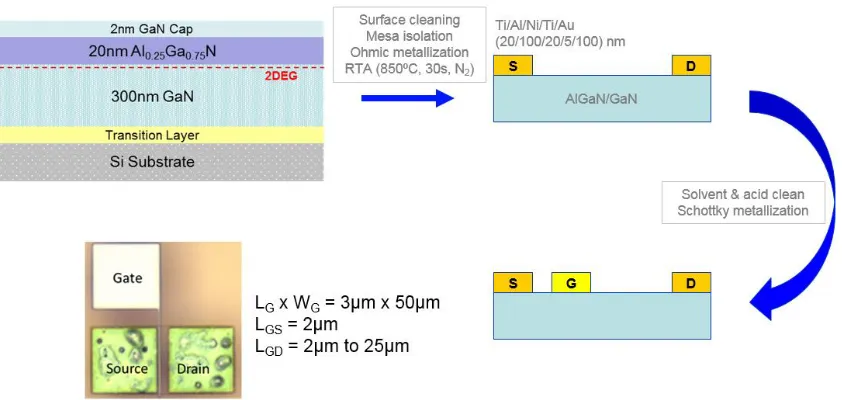
Substrate properties
Devices were fabricated on AlGaN/GaN heterostructure grown on Si <111> substrate, provided
by NTT Advanced Technology Corporation. Table 2.3 outlines the epi-layer structure. The GaN
cap improves dynamic reliability of the HFET device [108], [119], [120]. Figure 2.3 shows a
schematic of a typical substrate with Si (111).
Table 2.3: Epi-layer structure of the vendor substrate.
36
2.3.2
Surface cleaning
GaN surface is typically contaminated with high concentrations of structural defects, point defects,
surface contamination, and native oxide [101]. Gallium nitride forms a thin native oxide of mostly
Ga2O3 [109] in air ambient which impacts the dielectric/GaN interface for a deposited dielectric.
Cleaning and surface processing is therefore an important step in device fabrication. Multiple
surface cleaning techniques have been reported in literature with the most common chemical
cleans consisting of NH4OH or HCl followed by HF chemistries [110]. Furthermore, device
structure requires the deposition of a passivation scheme, gate dielectric, and/or ohmic contact on
the surface, which induces interface gap states as well as additional defect damage depending on
the deposition process. The GaN samples in subsections 2.3.3 and 2.3.4, whenever possible,
underwent solvent and acid clean to ensure the surface was kept as free of defects as possible. For
each of the process steps outlined below, with an exception of post-dielectric deposition, the
samples were exposed to acetone, methanol, isopropanol for 10 min each followed by HCl:H2O
(1:1) for 1 min and HF 1% for 1 minute. This clean process has been found to reduce the surface
carbon and native oxide concentrations [121].
2.3.3
HFET fabrication flow
The HFET fabrication process flowchart and animation are illustrated in Figure 2.4, and Figure
![Figure 1.1: Power electronics market expectation by Yole Développement [2].](https://thumb-us.123doks.com/thumbv2/123dok_us/1210138.1151995/19.612.125.487.505.688/figure-power-electronics-market-expectation-yole-developpement.webp)
![Figure 1.2: Theoretical on-resistance vs. blocking voltage capability for Si, SiC, and GaN based power devices [4]](https://thumb-us.123doks.com/thumbv2/123dok_us/1210138.1151995/20.612.124.476.403.632/figure-theoretical-resistance-blocking-voltage-capability-based-devices.webp)
![Figure 1.4: The Wurtzite geometric structure of GaN Crystal (a) Ga-faced and (b) N-faced [14]](https://thumb-us.123doks.com/thumbv2/123dok_us/1210138.1151995/23.612.136.479.445.646/figure-wurtzite-geometric-structure-gan-crystal-faced-faced.webp)
![Figure 1.6: (a) Net positive charge at the AlGaN/GaN interface caused by the sum of spontaneous and piezoelectric polarization [11] and (b) 2DEG formation and corresponding conduction band energy profile [95]](https://thumb-us.123doks.com/thumbv2/123dok_us/1210138.1151995/25.612.76.539.122.379/positive-interface-spontaneous-piezoelectric-polarization-formation-corresponding-conduction.webp)
![Figure 2.8: Simple schematic of the custom built pulsed-IV setup with an oscilloscope and a pulse generator [21]](https://thumb-us.123doks.com/thumbv2/123dok_us/1210138.1151995/63.612.84.531.72.272/figure-simple-schematic-custom-built-pulsed-oscilloscope-generator.webp)
![Figure 3.5: Comparison of two oxidants for (a) output characteristics (IDS–VDS), and (b) extracted specific on-resistance of the AlGaN/GaN MOSHFETs [16]](https://thumb-us.123doks.com/thumbv2/123dok_us/1210138.1151995/75.612.95.531.76.215/figure-comparison-oxidants-characteristics-extracted-specific-resistance-moshfets.webp)