FINITE ELEMENT METHOD SIMULATION OF PHOTOINDUCTIVE IMAGING FOR CRACKS C.-C. Tai and Y.-L. Pan
Department of Electrical Engineering National Cheng Kung University Tainan, Taiwan
Abstract—In this paper, the numerical simulations of photoinductive imaging (PI) method have been performed using the finite element method (FEM) with the 2D transient to characterize corner cracks at the edge of a bolt hole. The PI imaging results have higher spatial resolution in the area of the defect in 2D models as compared with the conventional eddy current (EC) images. The FEM simulation results of 0.5-mm rectangular defects are showed and analyzed. The dependencies of PI signals on EC frequencies and temperature of the thermal spot are also examined. The results demonstrate that the PI method is applicable to examine the geometric shape of corner cracks.
1. INTRODUCTION
Crack detection and sizing is a critical issue in quantitative nondestructive evaluation (NDE). The ultrasonic method is used predominantly to detect subsurface discontinuities, while the EC method is effective for surface cracks. However, one of the main disadvantages of conventional eddy current method is the low spatial resolution, which is constrained by the size of eddy current probes. The PI method is a hybrid NDE technique that combines eddy current and laser-based thermal wave methods. The use of a focused laser beam provides the method with a microscopic resolution while using eddy current pickup sensors.
equally well to characterize cracks on thick metals. Determining the crack dimensions is the interesting detection of a corner crack on the surface surrounding a bolt hole, such as depth and length [5].
In this article, we use the finite element method to simulate the photoinductive imaging (PI) technique for bolt-hole cracks inspection. Based on the simulation results, we also discuss the effects of EC frequencies and temperature of the thermal spot, and compare the PI results with EC images for a 0.5-mm triangular notch.
2. THE PHOTOINDUCTIVE IMAGING METHOD
Photoinductive mapping of eddy current fields interacting with cracks is a newly devised technique that is similar to photothermal (PT) imaging. The physical principles underlying it are illustrated in Fig. 1, which shows the coil of an eddy current probe carrying a current placed in close proximity to the specimen surface. A focused laser beam generates a localized hot spot on the specimen surface from above. The temperature fluctuation causes a local change in the electrical conductivity, which in turn induces a change in the impedance of the eddy current probe. The electrical conductivity of specimen is given by the expression:
σ = 1
[ρ0( 1 +α(T −T0))]
(1)
whereρ0 is the resistivity at temperatureT0, andαis the temperature
coefficient of the resistivity. T0 is the temperature 293 K, andT is the
actual temperature in the specimen sub-domain.
Figure 1. Inspection geometry of the photoinductive field measurement technique.
vector potential, A, which conforms to the following relation: (jωσ−ω2ε)A+∇ ×(µ−1∇ ×A) = σVloop
L , (2)
where ω denotes the angular frequency, σ the conductivity, µ the permeability, ε the permittivity, L the length, and Vloop the voltage applied to the coil. The conductivity outside the coil is zero. According to the constitutive relation (C.R.), the current density (Je) can be calculated as follows.
Je =σE=−σ
∇V +∂A ∂t
, (3)
where E is the electric field intensity. The electric potential (V) is obtained from Faraday’s law. The defining equation for the magnetic vector potentialA is a direct consequence of the magnetic Gauss’law. The induced current (I) in the coil is calculated by the integration of current density in the cross-sectional area (s) of the coil:
S
Je·ds=I. (4)
3. SPECIMEN AND SIMULATION
moving in the same direction as the previous case. The uniform scan plan with closely spaced scan lines so that flaw orientation and scan spacing would not affect the outcome was assumed. To calculate the impedance edance (∆Z = Vloop/I) of the coil in the simulations, the total induced eddy current of the coil can be obtained by carrying out sub-domain integration of the total current density for the cross-section of the excited coil.
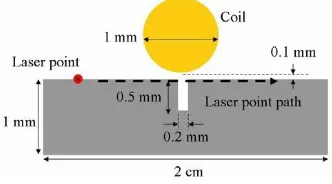
Figure 2. The actual size geometry of the 2D model for PI imaging method. (the bold dotted line is the laser point path).
Figure 3. The simplified 2D model for comparing the characteristics of PI imaging method and EC imaging method.
4. RESULTS AND DISCUSSION
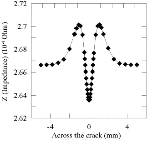
from 200 kHz to 1 MHz and the laser beam temperature from 100◦C to 500◦C. The diffusion of heat from laser beam and the eddy current density distribution around the crack are shown in Fig. 4. The temperature fluctuation causes a local change in the electrical conductivity of the specimen and the current density of the specimen. The lines indicate the contour of induced current density on the coil and the specimen. Figs. 5 and 6 show the signal of coil impedances with EC method and PI method, respectively. The center point of the rectangular notch is 0 mm in x-axis, as shown in Figs. 5 and 6. Fig. 5 is the EC image signals of a 0.5-mm rectangular notch at 600-kHz EC frequency, without laser beam. Fig. 6 is the PI image signals of a
0.5-Figure 4. The diffusion of heat from laser beam and eddy current density distributions. EC frequency, 600 kHz; laser temperature, 500◦C (773 K).
mm rectangular notch at the same EC frequency and 300◦C laser beam temperature. Because the length of the flaw is less than the diameter of the probe, the flaw scan produces a double-peaked response [6]. As shown in the Figs. 5 and 6, both figures conform to this phenomenon. Comparison of flaw impedance measured with two detection method for rectangular notch, the resolution of PI signal is higher than the EC signal. There is a higher sharp edge in PI signal than in EC signal.
Figure 6. The flaw impedances of PI signal for a 0.5-mm rectangular notch in Ti-6A1-4V. EC frequency, 600 kHz; laser temperature, 300◦C.
Figure 7. Images with different EC frequency. (EC scan without the laser beam).
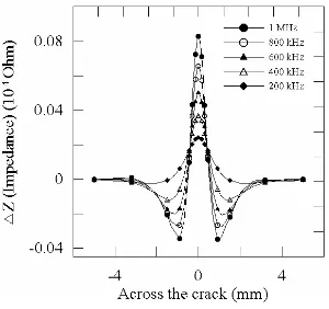
with crack and without crack is reported. As shown in Fig. 7, the eddy currents around the crack are more uniform at lower frequencies. But higher EC frequencies generate a stronger PI signal. Fig. 8 illustrates the signal amplitude is increased when higher eddy current frequencies are applied, and therefore the better crack images are obtained by increasing the eddy current frequency. Furthermore, the impedance difference for 200-kHz case is reversed on the notch area. That may due to deeper skin depth and lower current density on the surface of specimens. For the rectangular notches in this titanium alloy, eddy current frequencies above 200 kHz are more suitable for imaging the cracks.
Figure 8. PI imaging signal with different frequency. Laser temperature, 300◦C.
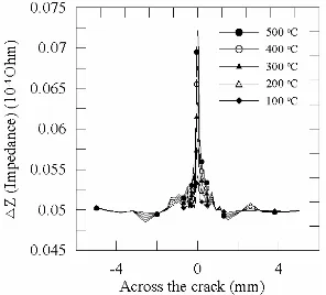
Figure 9 shows that the peak amplitude of PI imaging signals varies with laser point temperature for transverse scans across a 0.5 mm long and 0.2 mm wide notch. There is the same process to clearly display the crack’s shape. When lower laser beam temperatures are applied, the peak amplitude of signal is decreased. Because reducing the temperature will generates higher current density and deeper penetration on the surface of this specimen. That makes the eddy currents around the crack are more uniform at lower laser temperature.
5. CONCLUSIONS
The FEM simulation results demonstrate the feasibility of photoinduc-tive imaging method when applied to the detection of corner cracks. The EC frequency and laser beam temperatures affect PI signal am-plitude and resolution. The PI images have higher spatial resolution in the area of the defect in 2D models when compared with the con-ventional EC images. The higher PI signal amplitude can be obtained by increasing the laser beam temperature.
ACKNOWLEDGMENT
This research was supported by the grant from National Science Council, Taiwan (NSC 96-2628-E-006-256-MY3). Also, this work made use of Shared Facilities supported by the Program of Top 100 Universities Advancement, Ministry of Education, Taiwan.
REFERENCES
1. Moulder, J. C., N. Nakagawa, K. S. No, Y. P. Lee, and J. F. McClelland, “Photoinductive imaging: a new NDE technique,” Review of Progress in Quantitative NDE, D. O. Thompson and D. E. Chimenti (eds.), Vol. 8A, 599, Plenum Press, New York, 1989.
2. Moulder, J. C. and N. Nakagawa, “Characterizing the performance of eddy current probes using photoinductive field-mapping,”
Research in Nondestructive Evaluation, Vol. 4, 221–236, 1992. 3. Hughes, M. S., J. C. Moulder, M. W. Kubovich, and B. A. Auld,
“Mapping eddy current probe fields using the photoinductive effect,” NDT &E International, Vol. 28, 251, 1995.
5. Tai, C.-C. and J. C. Moulder, “Bolt-hole corner crack inspection using the photoinductive imaging method,”Journal of Nondestructive Evaluation, Vol. 19, 81–93, 2000.
6. Auld, B. A., S. R. Jefferies, and J. C. Moulder, “Eddy-current signal analysis and inversion for semielliptical surface cracks,”