INTERFACE AND
PDP-7 INTERFACE AND
INSTALLATION MANUAL
F-78A
3/66Chapter
2
3
4
5
CONTENTS
INTRODUCTION •••.•••.••.•..•....•..•.••••••..••••••••••••••••..•.•••
Programmed Data Transfers ...••••....••.••••.•.••.••...•••..••.• 2
Data Break Transfers ....•...•..•.•••.••..•••.•.•.••••.••••••••.••••• 3
Pertinent Documents
3
Logic Symbols ... • • • • . . . . • . . . • • • • • . . • • • . • • • . • . • • • . • • . • . • • • . • . • • • . . • • 4PROGRAMMED DATA TRANSFERS •.•....•.••...•••.•••••••.•••.••••.••.••
7
TimingCycle ..•.•••..••.•••••••••••••••••••.•••.•••••.•••••.•••.•• 10
lOP Generator .•...••••.•..•••.••••••••.•••••••...••••.•••••• 10
Device Selector (OS) .••••...•.•..• '. . . . • . • . • • . . • • • . • • . • • • . . • • • . . . • • • • 11
Slow Cycle Facility... 13
Input/Output Skip (lOS) ....•....•••••••••.•••..•••.•...•... 14
Information Collector (lC) •.•••..•••••••••••••..••.••...•....•.... 16
Information Distributor (10) .•.••.••.•.•• ••••••••••••••••••. .•••••••.•. 16 Data Transfers into the PDP-7 . . . • . . . . • . . • . • • . . . • . • • . . . • . • . • • . . . . • 18
Data Transfers out of the PDP-7 ...•.•..•••.•••••.••••••••••••.•.•..•. 19
Program Interrupt (Pi)... 19
Multiple Use of lOS and PI .... ...•••....••.... .•...•.• . .•• .•••••.•.•• 22
Example of Programmed Data Input and Output. . . • • . . . . • . • • • . • • • . • . • • 24
DATA BREAK TRANSFERS •...•••.•..••••.•...•.••.•••••••.••.•••••••..• 29
Data Break Fac
iI
ity ...•.•..•...•.••..••••••.•..•••..•..•... 31Data Address . . . • . . . • • . • . • • • • • . • • • • • . . • • • • • . . . • . . . • . . • . . . 33
Data Information Input and Output ...•...•.•...••..•••... 33
DIGITAL LOGIC CIRCUITS .••..•.••••••.•••••••..•.•..•.•••.•••••.•.•••. 37
Inverters ...•••••..••.•••...••..••.•.•..•••.•••••.•.••...•..•.•.... 37
Bus Drivers ...••.•....•...••••..••.•..••••.•.••..•.••••....•.•••... 37
Pulse Ampl ifiers ..•...•...•.•..•.•••••.•.••.. 38
Diode Gates •..•••...•.•....•..•.•.•••••.•.••...•.•.•••.•... , 39
INTERFACE CONNECTIONS •...•..••..•...•..••••..••••.••..•.•...
Interface Connections and Signal Identification
iii
41
CONTENTS (continued)
Chapter
5 (cont) Loading and Driving Considerations ••••••• ~ •••••••• • •• " ~. "0' • " • • •• • • • • • 43
Device Selector ••.•..•...••.• " ...••.•.••.•.• ...
0.
eo_ • • • • • • • • • • • • 73
Information Coil ector ••••••••••••••••••••••••••• " •• ',' • • • • • • • • • • • 74
I nformation Distributor ••••••••••••••• ',' • • • • • •• • • .. • • • • • • • • • • • • • • • 76
Power Clear Output Signals •••••• " • •• • • • • • • • • • •.• • .. • •• •.• • • • • • • • • • • 78
Begin Buffered Output Signal ... 78
RU,n Output Sig.nal ... 0" • : • • • • • • • • • • • 78
Slow Cycle Request Input Signal ••••••••••••••••••..• '.' • • • • • • • • • •• • 78
Program Interrupt Request Input Signal •••••••• ~ • • • • .• • •• • • . • • • • . • . • 78 Data Break Request Input Signal ••••••••••••••••••.• ••• • • • • • • • • . • • 79
Transfer Direction Input Signal •••••••••••••••••••••••••••••.••••• 79
Data Address Input Signal... •• • • •• .. • • • • • • • • • • • • • • ... • • • • • • • • • • 80
Address Accepted Output Signal •••••••••••••••••••••••••••••••••• 80
Data Information Input Signals ••••••••••••••••••••••••••••••••••• 80
Data Ac~epted Output Signal ••••••••••••••••• ,... 80
Data Ready Output Signal •••• , •••••••••••••••••••• -••••••• -. • • • • • • 80
Data Information Output Signals. • • • •• • •• • • • • • • • • • • • • • • • • • • • • • • •• • 81
6 INSTALLATION PLANNING 83
Physical Configuration •••••••••••••••••••••••••••••••••••••••••••••• 83
Environmental Requirements •••••••••••••••••••••••••••••••••••••••••• 83
Power Requirements. • • • • • • • • •• •• . • • • •• • • • • • . • •• • • . . . . • • • • • . • . • •• • •• • 86
Cabl ing Requirements .••••.•.•••••...•.••••.••••••••••.• ~ • • • • • • • • • • . 86
Appendix
PDP-7 DEVICE SELECTOR AND INFORMATION COLLECTOR
REQUIREMENTS FOR STANDARD OPTIONS ••••••••••••••••••••••••••••••• 89
ILLUSTRATIONS
Typical PDP-7lnstallation • ••• •••••••••• ••••••••• •••••• •.••••••••••••••••• vii
3
45
67
89
1011
12 13 14 15 16 17 18 19 20 21 2223
2425
2627
28
29 30 31ILLUSTRATIONS (continued)
Programmed Data Transfer Interface Block Diagram •••.• '" •.•••••..•••••....•
Decoding of lOT Instructions •..•..•.•••••••••••••••••.•••.•••••••••••••••
Programmed Data Transfer Timing Diagram •..•••.•.••..•••..•••..•••.•..•.••
lOP Generator ••.••..••.•••.•••••••••••••••••••••.•••••..••.••..•••.•••
Generation of lOT Command Pulses by Device Selector ••••.•••••••••..•••••.•
Typical Device Selector (Device 34) •.••••.•.••••••••••••••••.•••••.•••••••
Slow Cycle Facility •.•••..•••.••••.•••••••.•••••••••••.••••.•••.••.•••..
Input/Output Skip Fac
iI
ity •..•.•.•.••.••••••••••••••.••.•••••..•••••.••.•Information Collector and Information Distributor •••••••••••.••••.•••..••••••
Programmed Data Input Transfer ••.•..•.• " •.••••.•••.••••••••••••.••.••••...
Programmed Data Output Transfer ...•.•••••••.•.•••••••.•.••...••••••.
Program Interrupt Facility ..•••.••.•••.••.••••••.••••••••••.•.•••••.•••.•.
Multiple Use of lOS and PI ...••.•.••.•...•••••...•••••••• " ••••••••••••••..
Programmed Data Input Flow Diagram ....•.••••..•.•••••.•••....•••••••.•..
Programmed Data Output Flow Diagram .••.•••.•..•.•.••.•••••••..•.••••••.•
Data Break Transfer Interface Block Diagram •••..••••••••••••••••••••••••.•.
Data Break Transfer Timing Diagram .•...•••••..••. '" ••••••••••••.•••..•.
Data Break Fac
iI
ity I nterface of Computer .••..••••.•••••••••...••••....••••Data Address Input Interface of Computer ••.•...•••.•.•••••.•..••••.••••.•.•
Data Information Input and Output Interface of Computer ...•••••••••••.••••..
Inverter Circuit •...••••••••.•••.••••.•••••••.••••.•..••••.•..•..••.•••
Bus Driver Output Circuit .••..•..•..•••.•••••••••••••••.•••••••••...•.••.
Pulse Ampl ifier Output Circuit .•.•.••.•.••••.•..•.•••••••...••••••••••..•.
Diode Gate Circuit .••.•.•••••••.••••.••••.••••••••••••.•.•••••.•••.•.•.
Interface Cable Connector Locations and Assignments ••••••••••.•.••.••••....
Information Collector Channel Assignments ...•.••.•••...•..•••.•.•••••...••
Basic PDP-7 Component Locations ••.••.•..••••••.••.•••..••••.••••.••••.•.
Typical PDP-7 System Component Locations .••••••••••.•.•..••..••.••••••.•.
Basic PDP-7 Installation Dimensions •.•..••••••••....•..•..••.•...•...••..•
TABLES
Table Page
2
3
4
5
Input Signals .••••.•..••••••.•••••••••.••••••.•••••••.••..••..•...••.... 44
Output Signals ..••••.•••••••.•••••••.•.•.••••••••••.••.••••••••.•••••••
Prewired Interface Connections ••.•..•.•.•••••••••••••.••••••••••••••••.•.
lOT Code Assignments ••••••••••••••...••.••••••••••••.•.••....•••.•••••.
Installation Data ••.•••••••••••••••••.••...••••••••••••••••••••••.•••..••
57
64
75
CHAPTER 1
INTRODUCTION
Since the processing power of a computer system depends, in large measure, upon the range and number
of peripheral devices that can be connected to it, the Programmed Data Processor-7 (PDP-7) has been
designed with a very broad, flexible, and expandable interface. This manual defines the interface
char-acteristics of the computer to allow the reader to design and implement any electrical interfaces required
to connect devices to the PDP-7. This manual also provides information for planning the installation of
a PDP-7 system. Information in this manual applies only to PDP-7 systems with serial numbers above 100.
Refer to the PDP-7 Interface and Installation Manual, F-78, dated 1/66, for information on systems with
serial numbers below 100.
The PDP-7 is a digital machine designed for use as a general-purpose computer, an independent
informa-tion handl ing faci I ity, or as the control element in a complex processing system. The PDP-7 is a
single-address, fixed l8-bit word length, parallel processing binary computer using lis complement arithmetic
(21
s complement arithmetic faci I itates mu I tiprec i sion operations). Cyc Ie time of the random-access core
memory is 1 .75 jJsec, permitting a computation rate of up to 285,714 additions per second.
Programming features of the computer include indirect addressing, microprogramming (combining instructions
to occur in one 1 .75~sec machine cycle), and programmed monitoring of peripheral devices. Real-time features of the computer include program interrupt (entry into a subroutine caused by a request from an
I/O device), input/output skip facility (program flow modification as a function of the status of a selected
peripheral device), and high-speed data break channel (direct input/output access to computer core
mem-ory for cycle-steal ing data transfers at a rate of over 10 mi Ilion bits per second). Eight autoindex registers
simplify sorting, searching, and multiple input/output list processing operations. An operator console
pro-vides manual control and visual indication of programmed operations. An l8-bit switch register
per-mits manual entry of data and instructions, or status information to be sensed by the program. The console
displays all active registers, including the memory address register, memory buffer register, accumulator,
link bit, machine state, instruction register, program counter register, and multiplier quotient register of
the optional extended arithmetic element.
The basic PDP-7 system consists of a Type KAl7 A Processor, a Type 149 Core Memory, and a Type KAl1 A
TM
I/O Package composed of FLIP CHIP circuit modules and solid-state power supplies. These hybrid silicon
circuits have an operating temperature range exceeding the limits of 32° to 122°F, so no air-conditioning
is requ ired at the computer si te. Standard 115v, 60-cps power operates the computer. The basic system is self-contained in a 3-bay cabinet 69-1/8 inches high and 61-3/4 inches wide. This unit weighs
ap-proximately 1150 Ib, requiring no subflooring or bracing.
In addition to the standard tape reader, tape punch, and Teletype keyboard/re~ader, the PDP-7 system can operate over 64 input/output devices. Existing interface designs permit connection of a number of
DEC options to the computer, including devices such as line printers, magnetic: tape transports, magnetic
drums, card equipment, analog-to-digital converters, CRT displays, and digitClI plotters. The PDP-7
system can also accept other types of instruments or hardware devices that have an appropriate interface.
The simple I/O techniques of the PDP-7 allow inexpensive, straight-forward device interfaces to be
real ized. Any device interface needs control to determine when an information exchange is to take place
and to specify the location(s} in the computer core memory which accept or yield data. Either the
com-puter program or the transferring device may exercise this control. Transfers made under control of the
computer program are called programmed data transfers. Transfers made under control of the external
device are called data break transfers.
PROGRAMMED DATA TRANSFERS
The majority of I/O transfers occur under control of the computer program. The maximum real istic rate of
transferring 18-b it words is 33 kc in the program interrupt mode. Normally this speed is well beyond that
required for laboratory or process control instrumentation .. To transfer and stqre information under program
control requires about six times as much computer time as under data break control. In terms of real time,
the duration of a programmed transfer is rather small due to the high speed of the computer.
To real ize f~1I benefit of the built-in control features of the PDP-7 programmed I/O transfers should be
used in most cases. Controls for devices using programmed data transfers are usually simpler and less
expensive than controls for devices using data break transfers. Analog-to-digital converters,
digital-to-analog converters, digital plotters, I ine printers, message switching equipment, and relay control systems
typify equipment using the programmed data transfer channels.
Using programmed data transfer channels, simultaneous operation of devices is llimited only by the relative
speed of the computer with respect to the device speeds, and the search time required to determine the
device requiring service. The percent of computer time taken for I/O servicin!~ is roughly:
%1/0
time = sum of device rates (in cps) x service time (fJsec per interrupt) x 10-4For comparison, it takes less t-han 3% of computer running time to read or write conventional
DATA BREAK TRANSFERS
Devices which operate at very high speed or which require very rapid response from the computer use the
data break transfer channel. This channel permits an external device, almost arbitrarily, to insert or
ex-tract words from the computer core memory, bypassing all program control logic. Because the computer
program has no cogn izance of transfers made through this channel, programmed checks of input data are
made prior to use of information received in this manner.
The data break is particularly well-suited for devices that transfer large amounts of data in block form,
e. g., high-speed magnetic tape systems, high-speed drum memories, or CRT display systems containing
memory elements.
PERTINENT DOCUMENTS
The following publications serve as source material and complement the information in this manual.
1. Digital Logic Handbook, C-105. This book describes the functions and
specifica-tions of FLIP CHIP modules and module accessories used in the PDP-7, control interfaces,
and peripheral devices.
2. PDP-7 Brochure, F-71. This leaflet presents the basic functions of the PDP-7
hardware, software, instructions, and standard optional equipment.
3. PDP-7 Users Handbook, F-75. This book contains computer organization
in-formation, detailed information on the function of interface facilities, and
de-scriptions of the timing and operations performed by all instructions.
4. PDP-7 Maintenance Manual, F-77 A. This manual gives functional
descrip-tion, principles of equipment operadescrip-tion, interface, installadescrip-tion, operating
procedures, and detailed maintenance information for machines with serial numbers
above 100.
5. Instruction manuals for appropriate input/output device options used in PDP-7
systems are avai lable.
6. PDP-7 Price List, F-72. This leaflet contains current price information on the
basic computer, computer options, and standard input/output equipment.
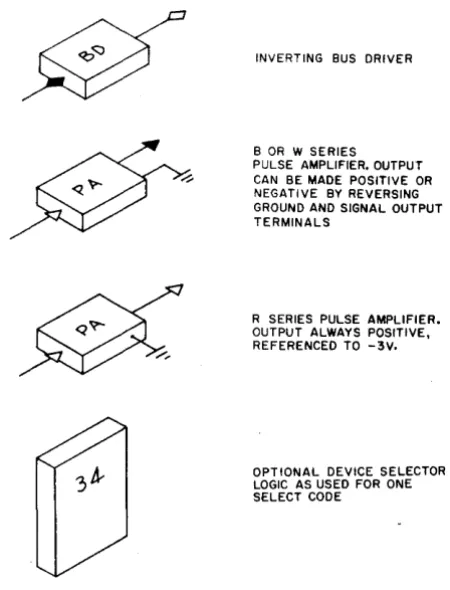
LOGIC SYMBOLS
Figure 2 defines the symbols used to express digital logic circuits and signals in the illustrations of this
manual.
4
- - { >
•
DEC STANDARD NEGATIVE PULSE
DEC STANDARD POSITIVE OR POSITIVE-GOING PULSE
DEC STANDARD NEGATIVE LEVEL
DEC STANDARD GROUND LEVEL
FLOW
-15V LOAD RESISTOR CLAMPED AT -?Iv
PNP TRANSISTOR INVERTER 1. EMITTER
2. BASE 3. COLLECTOR
LOGIC AND GATE FOR NEGATIVE SIGNALS WITH COMPLEMENTARY OUTPUT SIGNALS
LOGIC OR GATE FOR GROUND LEVEL SIGNALS WITH COMPLEMENTARY OUTPUT SIGNALS
LOGIC NAND GATE FOR NEGATIVE SIGNALS
DIODE-CAPACITOR-DIODE GATE 1. CONDITIONING LEVEL INPUT 2. TRIGGERING PULSE INPUT 3. PULSE OUTPUT
FLIP-FLOP (BISTABLE MULTIVIBRATOR) 1. GATED SET-TO-l INPUT
2. GATED CLEAR-TO-O INPUT 3. DIRECT CLEAR-TO-O INPUT 4,5 OUTPUTS
INVERTING BUS DRIVER
B OR W SERIES PULSE AMPLIFIER. OUTPUT CAN BE MADE POSITIVE OR NEGATIVE BY REVERSING GROUND AND SIGNAL OUTPUT TERMINALS
R SERIES PULSE AMPLIFIER. OUTPUT ALWAYS POSITIVE, REFERENCED TO -3V.
OPTIONAL DEVICE SELECTOR LOGIC AS USED FOR ONE SELECT CODE
Figure 2 Logic Symbols (continued)
[image:14.615.215.440.70.365.2]CHAPTER 2
PROGRAMMED DATA TRANSFERS
The PDP-7 is a parallel-transfer machine that collects and distributes data in bytes of up to 18 bits.
Figure 3 shows information flow within the computer to effect a programmed data transfer with input/output
equipment.
BITS 0-3
MEMORY BUFFER REGISTER
(MB)
BITS 15-17
BITS 6-11
lOP PULSES
.
..---.
IOP
GENERATOR
ACCUMULATOR REGISTER
(A C)
DEVICE SELECTOR
(OS)
IOT
COMMAND PULSES
SLOW CYCLE REQUEST
Figure 3 Programmed Data Transfer Interface Block Diagram
CONNECTIONS TO INPUT I OUTPUT
DEVICE
All programmed data transfers take place through the accumu lator, the 18-bit arithmetic reg ister of the
computer. The computer program controls the loading of information into the accumulator (AC) for an
output transfer, and for storing information in core memory from the AC for an input transfer. Information
in the AC for output transfer is power ampl ified and suppl ied to the bussed connections of many peripheral
devices by the information distributor (I D). Then the program-selected device can sample these signal
I ines to strobe AC data into a control or information register. Input data signals arrive from many
periph-eral devices at input mixer circuits of the information collector (IC), which transfers data into the AC.
In the input/output skip facil ity (lOS), command pulses from the device selector (DS) sample the condition
of I/O device flags. The lOS allows branching of the program based on the condition or availability
of peripheral equipment, effectively making programmed decisions to continUE! the current program or
to jump to another part of the program, such as a subroutine that services an I/O device.
The DS generates command pulses during execution of input/output transfer (lOT) instructions. All
in-structions stored in core memory as a program sequence are read into the memory buffer register (MB) to
be executed. The operation code in the four most significant bits (bits 0 through 3) of the instruction is
transferred into the instruction register (lR) and decoded to produce appropriate control signals. When
the operation code is recognized as an lOT instruction, the lOP generator produces time-sequenced lOP
pulsesasa function of the three least significant bits of the instruction (bits 15 through 17 in the MB). The
lOP pulses, with an I/O device selection code in bits 6 through 11 of the instruction, are suppl ied as bus
inputs to all gates of the DS. The gating circuits of the DS associated with a sp1ecific device are enabled
by the select code to regenerate lOPs as specific lOT command pulses. Figure.4 shows the decoding of an
lOT instruction and Figure 5 indicates the timing of the lOP and lOT pulses.
DEVICE CLEAR AC AT EVENT SELECTION TIME 1 IF BIT IS A 1 OPERATION CODE
70a = lOT INSTRUCTION
~ r-~
A
I
:<
I
:<
I :.: I :.: I
>:
I :.: I
'---y-'SUBDEVICE SELECTION
'---y-' "---y--' SUBDEVICE lOP PULSE SELECTION GENERATION CONTROL
Figure 4 Decoding of lOT Instructions
One lOT instruction can generate one, two, or three sequential lOT pulses. These command pulses are
des-ignated by the octal code of the twelve least significant bits of the instruction in which they are generated;
e.g., lOT 3401 (usually bits 4 and 5 are unused and are assumed to be O's unless. otherwise specified).
These lOT command pulses from the DS go to the lOS, the IC, and to a specific I/O device whose action
they control. In this manner, the program produces commands to transfer data into or out of I/O devices;
to cause the program to skip or not skip an instruction based on the condition of (In external device flag;
or to start, stop, or perform operations in devices controlled by a command pulse.
lOT instructions can use the normal computer cycle time of 1.75 Ilsec, or can occur in a slow cycle
ad-justed to the speed of the slowest I/O device. The device selector can be wired to cause entry into a
slow cycle for any device, when its select code is in the lOT instruction being executed. Figure 5 shows
the timing of command pulses for devices using the normal or slow cycle and the availability of the AC
-0
COMPUTER TIME TIMINr, PULSE GENERATOR COMPOSITE OUTPUT (70-NSEC PULSES}
GROUND -3 VOLTS
I ANY lOT INSTRUCTION (FETCH) CYCLE I
t
(1.75 MICROSECONDS) "I I I-120 I I I I -l I 120 I I
150 -l i -I NSEC I 120 --I t- I 150,.-j r-
i
NSEC 120 ,....-+j l-I NSEC I I I I NSEC I I I NSEC I I I I NSEC I I1-240 ...., I 1---640 NSEC----J..- 270- l /+:210..!.-240,..../ 1---640 NSEC--I-270-l !.-210,..! I NSEC I I I I NSEC I I NSEC I NSEC I I I NSEC I I NSEC I
T6 T7 TI T2 13 T4 T5 T6 T7 T1 T2 13 T4 T5 T6
I I J I I I I I I I I J J J J
T7 T3 T4 T5 T6 T7 TI T2 13 T4 T5 T6
MEfv'f)RY BUFFER
REGIS TE R OUTPUT NOT AVAILABLE AVAILABLE ~~25 NSEC
ACCUMULATOR DATA FOR OUTPUT TRANSFER ACCUMULATOR CLEARED FOR DATA INPUT TRANSFER IF MB 14 CONTAINS A 1
r'
lOP GENERATOROUTPUT IOP 2
(400-NSEC PULSES)
IOP4
NOT READY ~_T6+100 NSEC I-T4+20 NSFC
READY NOT READY READY GROUND
-3 VOLTS GROUND
-3 VOLTS GROUND
-3 VOLTS
T4+IOONSEC--+IL ______________________________________ ~
T5 + 20 NSEC--+ .... ! ________ -'
T7+20 NSEC-.... ! ________ -'
TI + 20 NSEC OF NE X T C YC L E - ! ' - -______ ---'
rIOT XXOI GROUND
t
-3 VOLTS T5+40 NSEC-!~ ______ --,
OPTIONAL DEVICE SELECTOR OUTPUT (400-NSEC PULSES)
lOT XX02 GROUND
T7+ 40 NSEC-! .... ________ -' -3 VOLTS
lOT XX09 GROUND
-3 VOLTS TI + 40 NSEC OF NEXT CYCLE--+ .... ! _______ -'
COMPUTER TIME TIMING PULSE GENERATOR COMPOSITE OUTPUT (70-NSEC PULSES) MEMORY BUFFER REGISTER OUTPUT ACr.uMULATOR DATA FnR OUTPUT TRANSFER ACCUMULATOR CLEARED FOR DATA INPUT TRANSFER IF MBI4 CONTAINS A 1
rop GENERATOR COMPOSITE OU' PUT (400-NSEC PULSES) OPTIONAL DEVICE SELECTOR COMPOSITE OUTPUT 1400-NSEC PULSES)
(0) NORMAL CYCLE
ANY lOT INTRUCTION (FETCH) CYCLE _I
I - - - (1.36 MICROSECONDS+2 PRESET PERIODS) I -J I.- 210
I 150 J I I 120 I I I I I I 120 I I 120 I NSEC
I NSEC I-- 120 NSEC-+j ~ I I -+j r-NSEC I -+j I"-NSEC I
1 I..., j4-NSEC I I 1 I PRESET ACCORDING TO SLOWEST I PRESET ACCORDING TO SLOWEST I I I 1 1 I
1-240~ I 1----640 NSEC~270 -I I'-;~0--r-- I/O DEVICE,! MICROSECOND ~ 110 DEVICE,I MICROSECOND ----! r----640 NSEC~N2;E~""" 1 I T6 NSEC T7 Tl T2 13 NSEC T4 T5 N EC T6 MINIMUM T7 MINIMUM TI T2 13 T4 T5 T6
J I J J J J I J I I I I I I I
GROUND
-3 VOLTS
T6 T7 TI T2 T3 T4 T5 T6 T7 TI T2 73 T4 T5
NOT AVA/LABI E ~325 NSEC
AVA/LABL E
NOT REACT' ~ T6+ 100 NSEC I-T4 .,...'0 NSEC
REAc~r
NOT READY T4+ tOO NSEC=-:;j
READY ' - - - '
GROUND I
-3 VOLTS T5 +20 NSEc-1 T7+ 20 NSEC-! T1+20 NSEC---I lOP I lOP 2 OF NEXT CYCLE rop 4
_:~~~~ T5+40 NSEC-I T7+40 NSEC-I TI+40 NSEC--I r IOT XXOI IOT XX02 OF NEXT CYCLE IOT XX04
( b) SLOW CYCLE
Devices which require immediate service from the computer program, or which take considerable computer
time to discontinue the main program until transfer needs are met, can use the program interrupt (PI) fac il ity.
In this mode of operation, the computer can initiate operation of
I/o
equipmEmt and continue the mainprogram until the device requests servicing. A signal input to the PI requestinH a program interrupt causes
storing of the conditions of the main program and initiates a subroutine to service the device. At the
con-clusion of this subroutine, the main program is reinstated until another interrupt request occurs.
TIMING CYCLE
Cycle time of an lOT instruction is either normal or slow, depending upon the device addressed (see
Figure 5). All devices use the normal cycle unless the device selector for the selected equipment is wired
to request a slow cycle.
The normal lOT cycle time is 1 .75 fJsec, or equal to a normal computer cycle. At computer time 5 (T5)
10Pl is produced, at time 7 (T7) IOP2 is produced, and at time 1 (Tl) of the next cycle IOP4 is produced.
Time 1 of the next cycle can be used for IOP4, since time 1 is normally used only to prepare to read the
next instruction into the
MB
from core memory; so the IR andMB
still contain the same information. The time from the start of 10Pl to the start of IOP2 is 450 nseci from the start of IOP2 to IOP4 is 150 nsec.If consecutive lOT instructions occur, the time from the start of IOP4 in the first instruction to the start
of IOP1 of the second instruction is 1 • 15 fJsec.
The slow lOT cycle time produces lOP pulses at the same computer times as during a normal cycle; however,
the delay between timing pulses is adjustable from a 1 fJsec to 4 fJsec. Under special conditions
modifi-cations to the delay modules can produce even longer time delays. In all cases, delays are set to
ac-commodate the slowest device using the slow cycle feature of the computer (this timing exists for all devices
requesting a slow cycle). A complete slow cycle requires a 3.36 fJsec minimum.
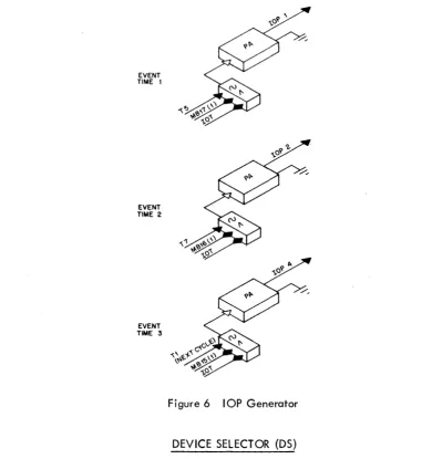
lOP GENERATOR
The logic circuits of the lOP generator are shown in Figure 6. When the instruction register decoder
detects an lOT instruction (the operation code in bits
MBO-MBS
= 111°
2), it generates the lOT signal. The lOT signal conditions one input of each of the three gates that trigger pulse ampl ifiers to produce
the lOP pulses. Each 3-input NAN D gate is operated by the condition of a bil" in the lOT instruction
and a computer timing pulse, to produce one of the sequential lOP pulses. Eac:h lOP pulse goes to one
gate of all device selector channels to allow generation of an lOT command pulse at one of the three
se-quential event times within the instruction. Figure 6 shows the computer timinH pulses and instruction bit
EVENT TIME I
EVENT TIME 2
EVENT TIME 3
Figure 6 lOP Generator
DEVICE SELECTOR (DS)
The DS selects an I/O device or subdevice according to the address code of the device specified in bits
4
through 13 of the lOT instruction. Selection of the device can request a slow cycle. The DS then
gener-ates lOT command pulses for each lOP pulse received, and transmits these commands to the
105,
the IC, and/or the device . Generally, lOT command pulses are used as follows:Command
lOT XX01
lOT XX02
lOT XX04
Use
Applied to the
105
to sense the condition of the device flag.Appl ied to the IC to transfer data into the computer I
or appl ied to the device to initiate a data transfer from the computer and clear device flags.
Appl ied to the device to initiate some operation (start, read, etc.).
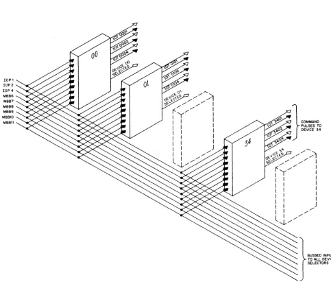
[image:20.613.125.515.51.465.2]Each group of these command pulses requires one channel of the DS, and each channel requires a different
address {or select code}. One device can, therefore, use several channels of the DS. Figure 7 shows
generation of command pulses by several channels of the DS.
[image:21.618.52.535.115.529.2]lOP 1 lOP2 lOP 4 MBBS MBS7 MSSS MBB9 MBSIO MBS11
Figure 7 Generation of lOT Command Pulses by Device Selector
}
COMMAND PULSES TO DEVICE 34
, /
I I I
I I
I
I
J
BUSSED INPUT TO ALL DEVICE SELECTORS
The logical representation for a typical channel of the DS, using channel 34, is shown in Figure 8. A
6-input NAND gate wired to receive the appropriate signal outputs from MB6-11 for select code 34
acti-vates the channel. In the DS module, the NAND gate contains 14 diode input terminals; 12 of these
con-nect to the complementary outputs of MB6-11, cmd 2 are open to receive subdevice or control condition.
signals as needed. Either the 1 or the 0 signal f~om each MB bit is disconnected by removing the appro-priate diode from the NAND gate when establishing the select code. The ground level output of the
for the device. This output also enables three gating inverters, allowing them "to trigger a pulse ampl ifier
if an lOP pulse occurs. The positive output from each pulse amplifier is an lOT command pulse identified
by the select code and the number of the initiating lOP pulse. Three inverters receive the positive lOT
pulses to produce complementary lOT output pulses. A pulse ampl ifier modu Ie can be connected in each
channel of the DS to provide greater output drive or to produce pulses of a specific duration required by
the selected device.
Figure 8 Typical Device Selector (Device 34)
SLOW CYCLE FACILITY
Up to twelve devices can request a slow lOT cycle by connecting the ground-level select signal output
of the DS channel to the slow cycle request facility. This facility consists of a 12-input diode NOR gate
for ground levels as shown in Figure 9. None of the basic PDP-7 input/output devices require a slow
cycle.
[image:22.615.110.553.182.540.2]LEVELS FROM DEVICE SELECTOR TO REQUEST SLOW CYCLE FOR UP TO 12 DEVICES
Figure 9 Slow Cycle Facility
INPUT/OUTPUT SKIP (lOS)
The condition of an I/O device flag and generation of an lOT pulse combine in the lOS to cause the program
to skip over one instruction. Incrementing the program count without executing the instruction at the current
program count causes skipping. The lOS facil ity consists of multiple 2-input ANID gates with outputs
con-nected in parallel to allow any gate to trigger the pulse ampl ifier which producc~s the 10 SKIP pulse. A flag or status level from the device and an lOT XX01 pulse from the appropriate channel of the DS provide
input connections to each gate as shown in Figure 10. In this manner an lOT instruction can check the
status of an I/O device and skip the next instruction if the device requires servicing. Programmed testing
in this manner allows the routine to jump out of a sequence to a subroutine that services the device tested.
Assuming that a device is already operating, a possible program sequence to test its availability follows:
Address
100, 101, 102,
Instruction
703401 600100 10XXXX
Remarks
/SKIP IF DEVICE 34 IS READY /JUMP .-1
[image:23.618.63.438.59.331.2]Figure 10 Input/Output Skip Facility
[image:24.615.148.500.42.679.2]When the program reaches address 100, it executes an instruction skip with 7034m. The skip occurs only
if device 34 is ready when the lOT 3401 command is given. If device 34 is not ready, the flag signal
disqual ifies the
105
gate, and the skip does no1" occur. Therefore, the program continues to the next in-struction which is a jump back to the skip inin-struction. In this example, the program stays in this waitingloop until the device is ready to transfer data, at which time the gate in the
105
is enabled and the skip occurs. When the skip occurs, the instruction in location 102 transfers program control to a subroutineto service device 34. This subroutine can load the AC with data and transfer it to device 34, or can load
the AC from a register in device 34 and store it in some known core memory address.
INFORMATION COLLECTOR (lC)
The information collector is a 7-channel gated Input mixer that transfers bytes of up to 18 bits into the AC
from signals suppl ied by an external device. Each channel consists of 18 2-input diode AND gates,
trig-gered by a common lOT command pulse from the DS. (Usually the lOT instruction that strobes information
into the AC via the IC is microprogrammed with bit 14 containing a 1.so that the:! AC is cleared at event
time 1 ~) Figure 11 shows the IC logic circuit configuration.
The perforated tape reader and I/O status bits each occupy one l8-bit IC channel. The teleprinter
occu-pies eight bits of a third channel. The remaining four and one-half channels are available for connection
to any peripheral and optional input equipment. Each PDP-7 input option connects directly into one or
more channels of the IC. For operation of more than seven input devices, the Ie is easily expandable in
blocks of seven channels to accommodate any number of channels.
INFORMATION DISTRIBUTOR (lD)
The I D is an output bus system that transfers information from the AC to external devices. Accumulator
output signals are buffered by 18 bus driver circuits and driven through cables to the I/O package. The
ID in the I/O package contains nine la-bit connection points, or channels, for each bussed signal; one
channel receives bussed connections from the processor, seven channels are avaiiable for individual
de-vice cable connections, and one channel is for external expansion of the ID. (The paper tape punch and
teleprinter receive AC output signals directly from the bus drivers and do not require connection through
the ID.) If all seven channels are used, the ID can be expanded to any number ()f output channels by
' J
INFORMATION DISTRIBUTOR IN I/O PACKAGE
Figure 11
ONE PAIR at;.RIPS
TERMINAfx~ANSION
::l
FOR 10 TER .... At').
~VEN
PAIRS :VICE~
- - STRIPS[g~NECTIONS
RMINAL STRIPS7 ...
~
CABLE __?NN~/6~~C~~G?~g~E~:O~~~~~
/ " U ),.
~
D)
CONNECTIONSInformation Collector and Information Distributor
[image:26.794.63.746.107.550.2]Figure 12 Programmed Data Input Transfer
DATA TRANSFERS INTO THE PDP-7
I
I
POP-71
EXTERNAL DEVICE
lOT XX02 and lOT XX04 command pulses control an external input device as indicated in Figure 12.
When ready to transfer data into the PDP-7 accumulator, the device sets a flag connected to the lOS.
The program senses the ready status of the flag and issues an lOT instruction to read the contents of the
external device buffer register into the AC. Usually this instruction contains a clear AC command and an
lOT XX02 (lOT XX12) to effect the transfer. If the AC is not cleared before the transfer, the resultant
word in the AC is the inclusive OR of the previous word in the AC and the word lrransferred from the
de-vice buffer register. To clear the AC prior to the transfer, bit 14 of the lOT instruction should contain
a 1. This microprogramming clears the AC at event time 1 (computer time T5), and an lOT XX12 pulse
[image:27.619.53.529.67.458.2]Following the transfer (possibly in the same instruction) the program issues an lOT XX04 command pulse
to initiate further operation of the device. This pulse also clears the device flag. For simpl icity, the
transfer path in Figure 12 shows only a single channel of the IC gates.
DATA TRANSFERS OUT OF THE PDP-7
lOT XX02 and lOT XX04 command pulses control an external output device as indicated in Figure 13.
The AC is loaded with a word (e. g., by a LAC instruction); then the lOT instruction is issued to transfer
the word into the control or data register of the device by an lOT XX02 pulse, and operation of the device
is initiated by an lOT XX04 pulse. The word transferred in this manner can be a character to be operated
upon, or can be a control word sampled by a status register to establish a control mode.
Connecting an output device to the PDP-7 interface adds at least three commands to the instruction
rep-ertoire. These commands use an lOT XX01 pulse to skip ·on the ready condition of the device flag, an
lOT XX02 pulse to effect a transfer from the AC to the device, and an lOT XX04 pulse to initiate
opera-tion of the device.
PROGRAM INTERRUPT (PI)
When a large amount of computing is required, the computer should process data rather than simply wait
for an I/O device to become ready to transfer data. The PI faci! ity, when enabled by the program,
re-I ieves the main program of the need for repeated flag checks by allowing re-I/O device ready flags to
auto-matically cause a program interrupt break. At the break location, program control transfers to a subroutine
which determines the requesting device and initiates an appropriate service routine.
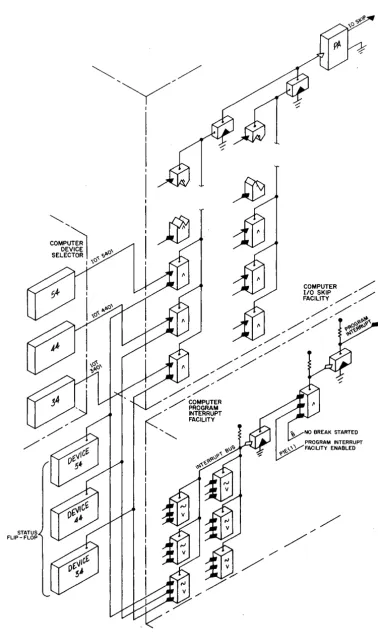
The basic PI faci! ity can accommodate interrupt requests from nine devices and is expandable. As shown
in Figure 14, the PI facility receives a negative signal from the flag of a device to request an interrupt.
This flag signal input to the PI can also connect to the
105
facility to allow the program interrupt sub-routine to detect the device requesting the interrupt if multiple devices are connected to the PI. OnFigure 14, note that any fI ip-flop or flag signal connected to an input of any of the six 3-input NOR
gates of the I/O package triggers the interrupt control circuits of the processor to cause a program
inter-rupt break, (if a break is not already in progress and if the interrupt system is enabl ed).
/
/\-~--/
... :>
0..
... :>
o
o
...
o
o
-0 <D
E
E
o
'-0>
o
'-Q..
<D
'-:>
0>
EXTERNAL DEVICE
COMPUTER PROGRAM rNTERRUPT FACILITY
I
COMPUTER
110 SKIP FACILITY
Figure 14 Program Interrupt Facility
NO BREAK STARTED
PROGRAM INTERRUPT FACILITY ENABLED
If only one device is connected to the PI facil ity I program control can be transferred directly to a routine
that services the device when an interrupt occurs. This operation occurs as follows:
[image:30.613.134.494.57.594.2]SR
Address
1000
1001
1002
0000
0001
2000
3001
3002
3003
1003
1004
Instruction
Remarks
/MAIN PROGRAM
/MAIN PROGRAM CONTINUES
/INTERRUPT REQUEST OCCURS
I NTERRUPT OCCURS
/LlNK, EXTEND AND TRAP FLIP-FLOP STATES,
/EXTENDED PROGRAM COUNT,
/ AND PROGRAM COUNT (PC==1003)
/ ARE STORED IN 0000
JMP SR
/ENTER SERVICE ROUTINE
/SERVICE SUBROUTINE FOR
/INTERRUPTING DEVICE AND SEQUENCE TO RESTORE
/AC, AND RESTORE LAND EPC IF REQUIRED
ION
/TURN ON INTERRUPT
JMP I 0000
/RETURN TO MAl N PROGRAM
/MAIN PROGRAM CONTINUES
MULTIPLE USE OF lOS AND PI
In common practice, more than one device is connected to the PI faci I ity. Therefore, since several devices
can cause an interrupt, the lOS must identify the device requesfing service. When an interrupt occurs, a
routine is entered to identify the device requesting an interrupt and to branch tel an appropriate service
routine. The device can be identified by lOT XXOl pulses that sample a device flags and causethe
pro-gram to branch or not branch according to the status. Figure 15 shows connecti()ns for three typical
de-vices. The following programming example illustrates these functions.
FLG CK
Address
1000
1001
1002
0000
0001
Instruction
Remarks
/MAIN PROGRAM
/MAIN PROGRAM COUNTINUES
/INTERRUPT REQUEST OCCURS
I NTERRUPT OCCURS
JMP FLG CK
lOT 3401
SKP
JMP SR34
lOT 4401
SKP
JMP SR44
lOT 5401
SKP
JMP SR54
/STORE LINK, EPC, AND PC
/(PC=1003)
/ENTER ROUTINE TO DETERMINE WHICH
/DEVICE CAUSED INTERRUPT
/SKIP IF DEVICE 34 IS REQUESTING
/NO - TEST NEXT DEVICE
/ENTER SERVICE ROUTINE 34
/SKIP IF DEVICE 44 IS REQUESTING
/NO - TEST NEXT DEVICE
/ENTER SERVICE ROUTINE 44
/SKIP IF DEVICE 54 IS REQUESTING
/NO - TEST NEXT DEVICE
COMPUTER /
110 SKIP ' . /
FACILITY / , " '
-' /
/ ,
~. / ' / ~Of:3~~~ ".- , ~i('i-~-:'
' /
~'/ ,
' /
/ ,
"
/
/ ,
" /
/ "
" /
/ "
" . / COMPUTER ,,"'- PROGRAM
(
INTERRUPT FACILITY
'''-...
I
I
I
II
I
I
I
I
Figure 15 Multiple Use of lOS and PI
23
[image:32.617.138.516.50.692.2]
Assume that the device that caused the interrupt is an input device (e. g., tape reader). The following example of a device service routine might apply:
Tag
SR
Instruction
DAC TEMP lOT XX12 DAC I 10 ISZ COUNT SKP
JMP END
LAC TEMP ION JMPIO
Remarks
/SAVE AC
/TRANSFER DATA FROM DEVICE BUFFER TO AC /STORE IN MEMORY LIST
/CHEC K FOR END /NOT END
/END. JUMP TO ROUTINE TO HANDLE END OF /L1ST CONDITION
/RESTORE LAND EPC IF REQUIIRED /RELOAD AC
/TURN ON INTERRUPT /RETURN TO PROGRAM
If the device that caused the interrupt was essentially an output device (receiving data from computer),
the lOT - then - DAC I 10 sequence might be replaced by a LAC I 10 - then - lOT sequence.
EXAMPLE OF PROGRAMMED DATA INPUT AND OUTPUT
The following example, explaining the function and connections of the Teletype unit and Type 649B
Teletype control, summarizes interfacing a device with programmed input and output data transfers, using
both program interrupt and I/O sk ip fac it ities. Figure 16 shows the sequence of operations for a transfer
into the computer from the keyboard, and Figure 17 shows the sequence for printing information transferred
out of the computer.
Assume that a program is in progress and the keyboard of the Teletype is manuall)' operated to send
infor-mation into the computer. When the key is struck, the control generates the 8-bit character and shifts
it into a keyboard buffer one bit at a time. When the character is complete in the register, the keyboard
flag is set to request a program interrupt. If the program interrupt is enabled (mean ing the program in
operation can be interrupted), when the flag is rclised a break occurs at the conclusion of the instruction
in progress. During the break cycle the contents of the link, trap mode bit, extended program counter
(EPC), and the program counter are stored at core memory address 000000, and the next instruction is
taken from address 000001 .
This instruction is usually a jump to an interrupt routine which checks the status of flags for all equipment
connected into the system. When this routine issues lOT instruction 700301, the 1 status of the keyboard
flag is identified and program control jumps to a subroutine that services the keyboard. This subroutine
OPERATING PROGRAM
BREAK REQUEST
BREAK GRANTED (PROGRAM INTERRUPT DIS-ABLED TO PREVENT OTHER INTERRUPTS FROM OCCUR-RING UNTIL THIS INTERRUPT IS COMPLETED)
CONTINUE PROGRAM
T
KEYBOARD OPERATIONS AND SUBROUTINES
I
I
I
~
Figure 16 Programmed Data Input Flow Diagram
25
[image:34.619.165.500.57.671.2]-~~--OPERATING PROGRAM
BREAK REQUEST
BREAK GRANTED
INITIALIZING COMMAND
CONTINUE PROGRAM
T
TELEPRINTER OPERATIONS AND SUBROUTINES
CLEAR TELEPRINTER
FLAG
I
~
I
[image:35.619.68.479.58.683.2]Octal
700312-06XXXX
20XXXX
700042
620000
Mnemonic
KRB
DAC I STORE
LAC AC SAVE
ION
JMPIO
Remarks
/CLEAR AC, THEN LOAD AC FROM CONTENTS
/OF KEYBOARD BUFFER, AND CLEAR KEYBOARD
/FLAG
/WRITE CHARACTER AT ADDRESS CONTAINED
/IN AUTOINDEX REGISTER IISTOREII
/RESTORE AC FROM LOCATION IIAC SAVEll
/ENABLE INTERRUPT SYSTEM FOR NEXT CHARACTER
/RETURN TO MAIN PROGRAM FROM ADDRESS
/STORED IN 00000 WHEN BREAK WAS STARTED
Upon completion of this subroutine the main program continues and the keyboard awaits the next manual
key operation.
Assume that the main program has accumulated and stored data in core memory, and that the data is to
be printed by the Teletype while the main program
conti~ues.When the program recognizes the need to
print, it initial izes a print subroutine (by setting an autoindex register equal to the core memory address -1
for the dater, establ ishing a check for the last character to be printed, initial izing a counter to track the
number of characters printed, etc.) and then enters the print subroutine to print the first character. The
basic print subroutine might be similar to the following:
Octal
Mnemonic
22XXXX
LAC I 10
44XXXX
ISZ COUNT
741000
SKP
60XXXX
JMP END
700406
TLS
700042
ION
620000
JMPIO
Remarks
/LOAD CHARACTER INTO AC FROM ADDRESS
/SPECIFIED BY AUTOINDEX REGISTER 10
/COUNT CHARACTERS
/NOT LAST CHARACTER
/LAST CHARACTER
/TRANSFER CHARACTER FROM AC INTO PRINTER
/BUFFER, CLEAR PRINTER FLAG, AND INITIATE
/PRINTING
/RESTORE LAND/OR EPC IF NECESSARY, THEN AC
/ENABLE INTERRUPT SYSTEM FOR NEXT CHARACTER
/BREAK
/RETURN TO MAIN PROGRAM FROM ADDRESS
/STORED IN ADDRESS 000000
Exit from this subroutine reestabl ishes the main program which now continues until interrupted by a
pro-gram break. Having been initiated by the subroutine, mechanical printing of the first character continues
until complete, then raises the print flag. The print flag in the 1 state indicates that the teleprinter has
printed the last character and is ready to receive another character, and requests a program interrupt.
Ifthe interrupt system is enabled, at the end of the current instruction the break state is entered to store the
contents of the L, EPC, and PC in address 000000. The next instruction is then taken from address 000001,
and program control is transferred to the interrupt routine. The program interrupt routine, as described
previously for the keyboard, senses the status of flags for all devices connected to the interrupt facility
until it determines the device requesting serViCE!. When the TSF instruction is given (lOT 700401) to skip
on the ready status of the printer flag, the print subroutine is again entered to load and print the next
character. At exit from the subroutine the main program is reentered from the point of the program break.
If the main program is an arithmetic routine that uses the I ink or a routine using extended memory, the
AC,
L,
and EPC must be restored by the device service routine prior to issuing the ION instruction. Res-toration of the L is accompl ished by an instruction sequence such as:Octal
200000 740010
Mnemonic
LAC 0
RAL
Remarks
/LOAD WORD CONTAINING L
/ROTATE TO RESTORE L
Restoration of the EPC is described in the PDP-7 Users Handbook, F-75, under the description of the
CHAPTER 3
DATA BREAK TRANSFERS
The data break facility allows one I/O device to transfer information directly with the PDP-7 core memory
on a cycle-stealing basis. Up to four dbvices can connect to the data break facility through the optional
Type 173 Data Interrupt Multiplexer.
Data break information transfers occur directly between the computer MB and a data register of the device,
and therefore do not affect the arithmetic or program control elements of the PDP-7. Transfer rates of up
to 571,000 words per second, or over 10 million bits per second, can be realized through this independent
data handling channel.
Figure 18 shows information flow to effect a data break transfer with an
I/o
device. Figure 19 indicates timing requirements for input and output control and data signals, and the availability of register datasignals. MEMORY ADDRESS REGISTER (MA) MEMORY BUFFER REGISTER (MB) DATA BREAK FACILITY DATA ADDRESS (15) DATA INFORMATION (18 BITS IN)
DATA INFORMATION
(18 BITS OUT)
ADDRESS ACCEPTED ..
...
DATA
ACCEPTED ..
...
DATA
READY ..
DATA BREAK ... REQUEST
:-" TRANSFER .... DIRECTION (IN)
~
CONNECTIONS TO INPUT I OUTPUT DEVICE
Figure 18 Data Break Transfer Interface Block Diagram
External devices requesting storage or retrieval access to core memory supply the following signals to
the computer:
DATA BREAK REQUEST
TRANSFER DIRECTION
DATA ADDRESS (15 bits)
DATA INFORMATION (18 bits)
- 3v for assertion
- 3v for into PDP-7, ground for out
- 3v for 1, ground for 0
- 3v for 1, ground for 0
w
o
COMPUTER TIME
DATA BREAK REQUEST
TRANSFER DIRECTION
DATA ADDRESS
NO REQUEST
REQUEST
NOT AVAILABLE
AVAILABLE
NOT AVAILABLE
AVAILABLE
~ 1.-,20 NSEC I ,
,- 600 NSEC
.'1
760 NSECa,.
390 NSEC . , . 600 NSEC al " - - 6 4 0 NSECa,
, I " I I ,
T5 T6 T7 Tl T2 T3 T4 T5 T6 T7 TI T2 T3
L _____ I _ I 1 I I I I I " ,
- --T I -~ - - - ----.- -- - - , - - - , - - ---T
LATEST POSSIBLE TIME
TO REQUEST A BREAK EARLIEST POSSIBLE TIME TO REMOVE REQUEST REQUEST MUST BE REMOvED BY T5 FOR THE NEXT CYCLE '.:...:'T~N~F ~DRES~ACCEP~D _ _ _ _ _ -.J IF NEXT CYCLE IS NOT TO BE A BREAK
- - - ,
LATEST POSSIBLE TIME TO DETERMINE DIRECTION IS T3 EARLIEST POSSIBLE TIME TO REMOVE DIRECTION IS AT END OF DATA ACCEPTED (IN) OR DATA READY (OUT)
~ ____________________________________ ~L _ _ _ _ _ _ _ _ _ _ _ _ _ _ _ _ _ _ _ _ _ _ _
LATEST POSSIBLE TIME TO DETERMINE ADDRESS iSTI- .,
OF BREAK EARLIEST POSSIBLE TIME TO REMOVE ADDRESS IS AT END OF ADDRESS ACCEPTED
NOTAVAILABLE - - - , - - - - - , i
DATA INFORMATION
I
LATEST POSSiBLE TiME TO DETERMINE - - , tEARLIEST POSSIBLE TIME TO REMOVE INPUT WORD (TO COMPUTER) INPUT WORD IS AT T3 IS AT END OF DATA ACCEPTEDAVAILABLE
-GROUND
ADDRESS ACCEPTED (70-NSEC PULSE)
DATA ACCEPTED (70-NSEC PULSE)
DATA READY (400-NSEC PULSE)
-3 VOLTS GROUND -3 VOLTS GROUND -3 VOLTS
u
I TIu
IT3
NOT AVAILABLE .
-DATA INFORMATION
!==
(FROM COMPUTER) T2+325 NSEC
AVAILABLE
NO BREAK
BREAK CYCLE
BREAK
I TI
I
[image:39.798.61.742.59.509.2]The computer provides the following signals to the device using the data break facility:
ADDRESS ACCEPTED
DATA ACCEPTED
DATA READY
DATA INFORMATION (18 bits)
Standard DEC 70-nsec negative pulse when
device-supplied address is strobed into MA.
Standard DEC 70-nsec negative pulse when'
device-supplied information is strobed into MB.
Standard DEC 400-nsec negative pu Ise when
information is avai lable in MB for strobing
by external device. The external device can
use this pulse to strobe the MB information into
its register either directly or (when gate set-up
time is required) after a delay of up to 1 !-,sec.
- 3v for 1, ground for 0
DATA BREAK FACILITY
The data break facility controls entry into the break state to execute a data break, and produces the
pulses that strobe address and data into the computer and indicate data is ready to be strobed out of the
computer. Figure 20 shows the interface circuits of the data break facility.
Data break requests are synchronized with the computer timing cycle and the execution of instructions
by a DATA SYNC flip-flop. The T5-DlY pulse (T5 delayed 50 nsec) sets this flip-flop if the DATA
BREAK REQUEST (or DATA RQ) signal level is at - 3v (making a request), or clears it if the request is
not made (signal level is at ground). When set, the DATA SYNC flip-flop causes generation of a BK RQ
(or BREAK REQUEST) signal level that establishes the break state for the next cycle if the current cycle
completes an instruction. Therefore, to initiate a data break the DATA BREAK RE QUEST signal must be
present (negative) at the time the T5-Dl Y pulse occurs during the cycle immediately preceding the break.
Similarly, when the break is granted the DATA BREAK REQUEST signal must be removed (ground or open)
by the time the T5-DlY pulse occurs or the next cycle will also be a break state.
Note that a break state (but not a data break) can also be caused by a program interrupt (PROG SYNC (1)
signal) or by the real-time clock (ClK SYNC (1) signal).
The 1 status of the DATA SYNC flip-flop combines with the break condition of the major state generator
to produce a DATA. B signal level that enables generation of the ADDRESS ACCEPTED (or ADDR ACC),
DATA ACCEPTED (or DATA ACC), and DATA READY (or DATA RDY) pulses.
The 70-nsec negative ADDRESS ACCEPTED pu Ise occurs at T1 time of all data break cyc les to strobe the
15 device-supplied DATA ADDRESS signals into the computer MAand EMA (extended MA) registers.
This pulse, available at the interface, can be used by the device to remove the DATA BREAK REQUEST
signal or to clear or change the data register in preparation for the next cycle.
The 70-nsec negative DATA ACCEPTED pulse occurs at T3 time of the data break cycle if the
device-supplied TRANSFER DIRECTI'ON signal level is at - 3v to specify a data direction into the computer.
This pulse strobes the 18'devic,e-supplied DATA INFORMATION signals into the MB and is available at
the interface for use by the device to clear and/or change the data buffer register for the next cycle.
The direction of a dat<:J break transfer is always ,stated with respect to the computer. The TRANSFER
DIRECTION signal should be - 3v to specify a tra'n'sferinto the PDP-7, or should be ground to specify
a transfer out of the PDP-7. This signal should be
presen~(:1t th~
time the data break request is mode;however, it need not be present unti I T3 of the break cy<;:I,e.'
The 400-nsec negative DATA READY pulse occurs at T3time of all data break cycles. This pulse is not
used in the computer but is produced for the device to u,se directly, or delayed to allow for gate setup
time, to strobe the 18 computer DATA INFORMATION signals into its data buffer register.
DATA ADDRESS
Fifteen DATA ADDRESS (or DA) signals are recieved from the external device to specify the core memory
address to be used for the data break transfer. These signals are - 3v to signify a binary 1. They shou Id
be present when the data break request is made, but may be delayed if they are settled prior to T1 time
of the break cycle. These sign~ls'are received by'a2-input NAND gate at the 1 input of each MA
flip-flop and extended MA flip-flip-flop. Since the MA contains 13 bits, the flip-flip-flops are designated MAS through
MA17. The two extension fl ip-flops are added to the IT,Iost significant end of the register and are
de-signated EMA3 and EMA4. Each of these flip-flops is loaded with the information on the DATA ADDRESS
lines suppl ied by the device when the ADDRESS ACCEPTED pu Ise occurs. The data break fac
iI
itygen-erates the ADDRESS ACCEPTED pulse at T1 time of a break cycle caused by a negative DATA BREAK
REQUEST signal. Figure 21 shows this data address interface logic of the computer.
DATA INFORMATION INPUT AND OUTPUT
Input data from an external device is received by the MB during a data break as 18 DATA INFORMATION
(or DI) signal levels. The DATA INFORMATION input signals should be present when the data break
request is made, but can be delayed if they are settled prior to T3 time of the break cycle. Each - 3v
signal (binary 1) enables a 2-input NAND gate at the 1 input of an MB flip-flop. The DATA ACCEPTED
pulse strobes all these gates. This pulse is generated in the data break facility at T3 of the break cycle
by negative DATA BREAK REQUEST and TRANSFER DIRECTION signals which request an input data break.
Figure 22 shows the data information input interface to the MB.
Figure 21 Data Address Input Interface of Computer
Output data from the computer during a data break is supplied to the external device as an- l8-bit MB
buffered DATA INFORMATION word. The negative binary 1 output of each MB flip-flop is buffered by
a non-inverting bus driver and supplied to the interface connection for strobing by the device. The
DATA INFORMATION signals are available by T3 time of the break cycle and must be strobed by the
DATA READY pulse (or a pulse derived from it) no later than 400 nsec after T2 time of the cycle
[image:43.619.38.550.113.478.2]Figure 22 Data Information Input and Output Interface of Computer
[image:44.620.83.589.61.402.2]