for Optoelectronic Device
Applications
A thesis by
Vinod Kumar Gupta
Submitted to the University of London for the Degree of Doctor of Philosophy and Diploma of Imperial College.
Physics Department
All rights reserved
INFORMATION TO ALL U SE R S
The quality of this reproduction is d ep en d en t upon the quality of the copy subm itted.
In the unlikely even t that the author did not sen d a com plete manuscript and there are m issing p a g e s, th e se will be noted. Also, if material had to be rem oved,
a note will indicate the deletion.
uest.
ProQ uest U 643123
Published by ProQ uest LLC(2015). Copyright of the Dissertation is held by the Author.
All rights reserved.
This work is protected against unauthorized copying under Title 17, United S ta tes C ode. Microform Edition © ProQ uest LLC.
ProQ uest LLC
789 East E isenhow er Parkway P.O. Box 1346
Abstract
In this thesis growth on patterned substrates has been studied for the lateral bandgap control of the quantum well (QW) structures, utilising indium migration from the side facets onto the adjoining (1 0 0) surfaces, leading to the possibility of integration of multi
functional optoelectronic devices. InGaAs/GaAs/AlGaAs single quantum well (SQW) lasers and InGaAs/InAlAs QW heterostructures were grown by molecular beam epitaxy (MBE) on (100) GaAs and In? substrates respectively, patterned to produce (100) mesa top surfaces with angled side facets. Chemical beam epitaxy (CBE) was used for the growth of InGaAs/InP heterostructures over In? substrates, patterned into undercut mesas with (100) top surfaces using chemically assisted ion beam etching (CAIBE).
Indium migration behaviour was compared by growing two InGaAs/GaAs/AlGaAs SQW graded index separate confinement heterostructure (GRINSCH) lasers by MBE over patterned GaAs substrates. The first laser was grown using As: throughout, whereas the active region of the second laser was grown using As4. It is observed that the use of As4
facilitates the migration process whilst the use of Asi completely stops it. However, the broad area devices of both lasers exhibit extremely low threshold current densities and very high external quantum efficiencies. Split contact devices were made by growing InGaAs/GaAs/AlGaAs SQW GRINSCH lasers by MBE over variable step width mesas patterned on GaAs substrates using a newly designed mask. Electrical measurements on partially pumped devices showed bistability or pulsation behaviour depending on the bias conditions on the unpumped section.
Growth of InGaAs/InP heterostructures by CBE on undercut mesas showed facetting behaviour producing atomically flat (Ill)B planes. Complete triangular shape structures bounded by very smooth ( lll) B facets were produced on mesas as narrow as
2 .0 pm. This shows the strong possibility of growing one dimensional (ID) quantum
Table of Contents
Title...1
A bstract... 3
Table of C ontents... 5
Acknowledgements... 9
Introduction... 11
1. Optical Properties of Low Dimensional Structures...15
1.1 Introduction...15
1.2 Band Structure in III-V Semiconductors... 16
1.2.1 Envelope Function Approximation...20
1.2.2 Density of States... 22
1.3 Optical Transitions... 24
1.3.1 Band-to-Band Recombination... 26
1.3.1.1 Matrix Element... 28
1.3.1.2 Oscillator Strength...29
1.3.2 Excitonic Effects... 29
1.3.2.1 Bulk Semiconductors...30
1.3.2.2 Quantum Wells... 31
1.4 Optical Characterisation...32
1.4.1 Photoluminescence (PL)...33
1.4.1.1 Effects of well width fluctuations...35
1.4.1.2 Effects of alloy fluctuations...36
1.4.2 Photoluminescence Excitation (PLE)...36
1.4.3 Time Resolved Photoluminescence (TRPL)... 37
1.4.4 Cathodoluminescence...38
1.5 Optical Devices...39
1.5.1 Quantum Well Lasers...39
1.5.1.1 Gain and Threshold Current Density... 41
1.5.2 Optical Modulators... 48
1.5.3 Split Contact Devices... 50
1.5.3.1 Wavelength Tuning... 51
1.5.3.2 Passive Modelocking...53
1.6 Conclusions...55
1.7 Reference...56
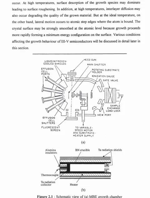
2. Epitaxial growth of III-V Compound Semiconductors...59
2.1 Introduction...59
2.2 Molecular Beam Epitaxy (MBE)...60
2.2.1 Growth Process...60
2.2.2 Growth Dynamics... 63
2.2.3 Growth of III-V Compounds... 65
2.2.3.1 Effects of Substrate Temperature...6 8 2 2 3 2 Effects of Arsenic Flux... 69
2.2.4 Dopants...70
2.2.5 Advantages and Disadvantages of MBE...71
2.3 Chemical Beam Epitaxy (CBE)...72
2.3.1 Growth Mechanism... 72
2.3.2 Growth of GaAs/AlGaAs Heterostructures...73
2.3.3 Growth of InGaAs/InP Heterostructures...75
2.3.4 Advantages and Disadvantages of CBE...76
2.4 Metal Organic Chemical Vapour Deposition (MOCVD)...76
2.4.1 Growth Process...77
2.4.2 Growth of III-V Compounds and... 78
Multilayer Structures 2.5 Conclusions...79
2.6 References...80
3. Patterned Substrates Overgrowth... 83
3.1 Introduction...83
3.2.1 Adatom Migration...8 6
3.2.2 Optoelectronic Device Applications...89
3.2.3 Optimum Growth Conditions...92
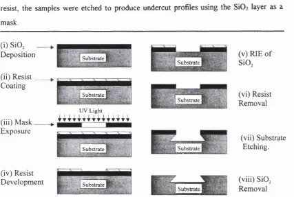
3.3 Substrate Patterning...96
3.3.1 Substrate Cleaning... 97
3.3.1.1 Solvent Cleaning... 97
3.3.1.2 Plasma Etching...98
3.3.2 Photolithography... 98
3.3.2.1 Resist Coating... 99
3.3.2.2 Exposure...100
3.3.2.2 Development...101
3.3.3 Wet Chemical Etching...102
3.3.4 Dry Etching...105
3.3.4.1 Reactive Ion Etching (RIE)...106
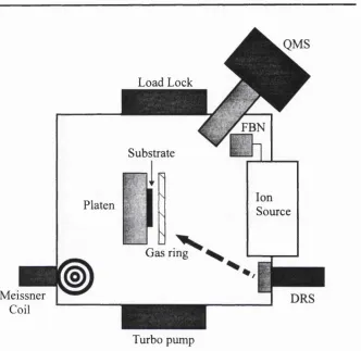
3.3.4.2 Chemically Assisted Ion Beam Etching (CAIBE)...108
3.3.5 Resist Removal...112
3.3.6 Pre-Growth Cleaning...113
3.3.6.1 Cleaning Process for GaAs Substrates...113
3.3.6.2 Cleaning Process for InP Substrates... 114
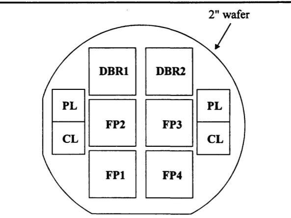
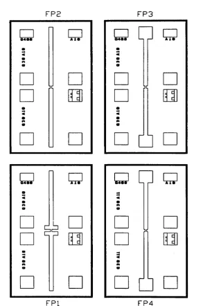
3.4 Mask Design...114
3.4.1 Regrowth M ask...114
3.4.2 Device Mask...123
3.5 Conclusions...127
3.6 References...127
4. GaAs Based QW Devices Epitaxially Grown o n ...129
Patterned Substrates 4.1 Introduction...129
4.2 Experimental Arrangement...130
4.2.1 Light Source...130
4.2.2 Monochromator...132
4.3 InGaAs/AlGaAs SQW Lasers Grown by MBE...136
4.3.1 Layer Structure...137
4.3.2 Growth Conditions...138
4.3.3 PL/PLE Spectra...138
4.3.4 Evidence of Photonic Coupling...143
4.3.5 Carrier Escape and Photon Recycling...145
4.3.6 Broad Area Devices...146
4.4 InGaAs/AlGaAs Split Contact Devices...152
4.4.1 Fabrication Process...152
4.4.2 Easing Characteristics...157
4.4.3 Bistability and Self Pulsation...159
4.5 Conclusions... 164
4.6 References... 164
5. InP Based QW Structures Epitaxially Grown o n ... 167
Patterned Substrates 5.1 Introduction... 167
5.2 Experimental Arrangement...168
5.3 The InGaAs/InAlAs System...170
5.3.1 Layer Structure...170
5.3.2 PL and CL Characterisation...171
5.3.2 Simple Analytical Model...176
5.4 Selective Area Epitaxy of InGaAs/lnP...178
5.4.1 Substrate Patterning...181
5.4.2 Growth Conditions...181
5.4.3 Structural Characterisation...182
5.4.4 Optical Characterisation...189
5.5 Conclusions... 193
5.6 References... 193
Acknowledgement
It gives me great pleasure to express my sincere gratitude to all those who have provided help, inspiration, and encouragement during the course of this project. First, 1 would like to thank Professor R.A.Stradling for offering me a studentship at the Solid State Experimental Group and for his encouragement in getting a Commonwealth Scholarship. This project has been completed in collaboration with the Institute for Microstructural Sciences, National Research Council, Ottawa, Canada. 1 would like to thank the Director General of the IMS, Dr. Peter Dawson, for inviting me to use institute’s facilities and for the financial support during my stay in Canada. 1 am eternally indebted to Dr. Robin Williams for his invaluable help, brilliant ideas and excellent supervision throughout this project at both places.
1 could not have completed this thesis without the help of Dr. Keith Bamham, who stepped in for Robin when he left Imperial College, and went out of his way to find additional funding when times were hard. 1 also thank him for supervising my thesis in
the final stages.
Thanks to Dr. Andrew Pratt (Oki Electricals Ltd., Tokyo) for all his initial help and fruitful discussions and with whom 1 enjoyed working. 1 am also thankful to Dr. Carl Norman (Toshiba Cambridge Research Centre Ltd., Cambridge) for his involvement in the project and for doing extensive CL measurements. Thanks to Dr. Ray Murray for lending his expertise whenever 1 approached him and allowing use of his laboratory
facilities to do some experiments when my experimental setup was moved to Canada.
(SiGe Microsystems Inc., Ottawa) for providing me his expertise in operating the MBE machine.
Thanks to many friends in the Experimental Solid State Group for their general help, discussions and for their friendship. In particular, I would like to name a few : Dr. Mark Pullin, Dr. K. Vodopyanov, Dr. Vassilis Chazapis, Harvey Hardaway, Jôrg Heber, Dr.Jenny Nelson, Dr.Jenny Bames, Dr.James Connolly, Steve Webb, Paul Griffin, Ian Ballard, Ned Ekins-Daukes, Nish Malde, and Brendan Serapiglia. My special thanks are due to Phil Davies for many helpful discussions. Last but certainly not the least, many thanks to Jean Leveratt and Derek Podger for all the cheerful conversations we had.
The Commonwealth Scholarship Commission and the British Council have helped over the years with financial support, assistance with academic and practical problems, and administrative help. I thank them for this invaluable and all encompassing approach. I would also like to thank the Ministry of Human Resources and Development, Government of India for administrative help and the Board of Governors of the Bundelkhand Institute of Engineering and Technology, Jhansi (India) for granting me study leave.
I would never be able to thank enough to my parents, brother and sister who have always encouraged me to do my best and who have given me tremendous love and affection. I owe a great debt to them for bearing the pain of our separation.
A major objective in the field of semiconductor optoelectronics is the integration on a single semiconductor substrate of many diverse device functionalities. For the growth of III-V semiconductor heterostructures using molecular beam epitaxy (MBE), a particularly effective technique to facilitate this integration is that of growth on patterned substrates. This technique utilises variations in the growth rate on different crystal planes which are associated with different effective incorporation coefficients and geometric considerations due to the directional beam nature of MBE. ^ Additionally, by suitable design of patterned mesas, interplanar adatom migration from side facets onto the (1 0 0) growth surface can produce controlled lateral patterning of quantum well
(QW) heterostructures.^’^ Such lateral control allows optimised variations in energy bandgap and index of refraction which can be exploited for the integration of many optoelectronic devices such as laser/passive waveguide, laser/modulator or segmented contact mode-locked lasers.
This thesis deals primarily with an investigation of growth on patterned substrates with the aim of fabricating ‘Split Contact Devices’ for optoelectronic device applications. Strained InGaAs/GaAs QW lasers have the potential advantage of low threshold current and high differential quantum efficiency, making them suitable for optoelectronic integrated circuits (OEICs). In addition, by varying the amount of indium and the thickness of the QW , the emission wavelength can be tuned between 870 nm -1100 nm for a number of interesting applications including 980 nm pumps for Er^^-doped fibre amplifiers and 1060 nm high power pumps for frequency doubled blue-green lasers. For the growth of strained InGaAs/GaAs QWs on patterned substrates by MBE using arsenic tetramers (As^) as the group-V source material, previous studies have indicated that the indium migration process is very sensitive to the specific growth conditions, in particular the substrate temperature and the group-V flux."^ It has been shown that
indium migration can be controlled by choice of the arsenic flux during growth of a multi-quantum well (MQW) structure on a variable step width mesa, leading to the possibility of integrated structures in which not only the bandgap but also the effective
number of active quantum wells is controlled from region to region/
In the present work a further investigation of indium migration behaviour has been carried out by changing the nature of the arsenic species from arsenic tetramers (As^) to arsenic dimers (AS2) during the growth of InGaAs/GaAs QWs on (100) GaAs substrates
patterned into ridges and grooves. A completely different migration behaviour is observed when arsenic is supplied in the form of AS2 by cracking As^ molecules at high
temperature in a valved cracker attached to the arsenic cell. We have also compared the luminescence behaviour and lasing properties of two InGaAs/GaAs/AlGaAs single quantum well (SQW) graded index separate confinement heterostructure (GRINSCH) lasers where the first laser was grown using As2 throughout and the second was grown
using As2 for everything except the active region which was grown using As^.^ Both
lasers exhibit extremely low threshold current density, very high internal quantum efficiencies and very low internal losses.
Split contact, ridge waveguide, devices have been fabricated using a mask system which was designed to produce devices with variable mesa widths for different lengths of the gain and absorber sections. The observed bistable behaviour in the light-current (LI) characteristics of these devices show their possible use in memory applications or fast switching devices.
excess of 70 meV7 Low temperature photoluminescence (PL) and cathodoluminescence (CL) characterisation of InGaAs/InAlAs QWs grown on patterned InP substrates reveal an emission peak corresponding to the facet intersection with the (100) surface. One important observation with respect to this emission is that the peak position remains invariant irrespective of the width of the patterned mesa. A simple analytical model based on diffusion of growth species has been developed which utilises this particular emission from the facet intersection to calculate the effective flux and relative increase in indium concentration at different points on the mesa top. Good agreement between the experimental and calculated values has been observed.
Recently, quantum wire (QWR) structures with quasi-one dimensional (ID) quantum confinement of charge carriers have attracted wide interest due to their unique optical properties. Very large exciton binding energy, modified electro-absorption and electro refraction spectra, enhanced optical non-linearities and optical gain make these structures very useful for applications in many novel optoelectronic devices*. The higher optical gain and narrower spectral gain profile make it possible for QWR lasers to operate at extremely low threshold currents and show reduced temperature sensitivity and higher modulation speed.^ However, the fabrication of such structures on a nanometer scale is extremely difficult. One of the important requirements to achieve efficient luminescence from QWRs is the formation of defect free smooth interfaces. To achieve this objective, fabrication techniques in which wires are formed completely in-situ seem attractive. Previously, GaAs wires have been successfully formed completely
in-situ in V-grooved substrates.'^ Alternatively, facets may be formed in-situ and overgrown. We have used chemical beam epitaxy (CBE) to generate (111)B facets completely in-situ through the growth of InGaAs/InP layers on undercut InP mesas patterned by chemically assisted ion beam etching (CAIBE). Atomically flat facets have been generated and an attempt has been made to grow InGaAs wires just before the completion of inverted-V shape structures on patterned InP substrates.
techniques routinely used for the growth of semiconductor devices. The technique of growth on patterned substrates is reviewed in chapter 3. Substrate patterning, mask design, wet chemical etching and photolithography are also within the content of chapter 3. Results for GaAs based quantum well structures and devices are described in chapter 4. Chapter 5 describes the characterisation of structures grown on InP substrates. Finally conclusions and future recommendations are drawn in chapter 6.
References
^ W.T.Tsang and A.Y.Chao, Appl. Phys. Lett., 55 (6), 293 (1977).
^ S.Nilsson, E.Van Gieson, D.J.Arent, H.P.Meir, W.Walter and T.Forster, Appl. Phys. Lett., 55(10), 972(1989).
^ D.J.Arent, S.Nilsson, Y.D.Galeuchet, H.P.Meir and W.Walter, Appl. Phys. Lett., 55 (25),2611 (1989).
^ A.R.Pratt, Ph.D. Thesis, University of London (1995).
^ A.R.Pratt, R.L.Williams, C.E.Norman, M.R.Fahy, A.Marinopoulou and F.Chatenoud, Appl. Phy. Lett., 65 (8), 1009 (1994).
^ M.Dion, V.K.Gupta, Z.R.Wasilewski, C.E.Norman, A.R.Pratt, P.Chow-Chong and R.L.Williams, Procd. Of 15* IEEE - ISLC Conf., Haifa, Israel ( 1 3 - 1 8 Oct. 1996 ). ^ V.K.Gupta, R.L.Williams, Z.R.Wasilewski, M.Dion, G.C.Aers and C.E.Norman, Procd. IEEE - LEGS’96 Annual Meeting, Boston, Massachusetts ( 1 8 - 2 1 Nov. 1996 ). * H.Sakaki, Surf. Sci. 267, 623 (1992).
^ Y.Arkawa, and A.Yariv, IEEE J. Quantum Electron. 22, 1887 (1986).
DIMENSIONAL STRUCTURES
1.1 Introduction
With the advent of growth techniques such as molecular beam epitaxy (MBE) and metal organic chemical vapour deposition (MOCVD), it is now possible to grow very thin semiconductor heterostructures with monolayer precision. The reduced dimensionality of these structures has many important consequences for the electronic and optical properties of the material due to quantum confinement of charge carriers. The simplest structure which is most commonly used in many optical devices consist of a thin layer of a narrow bandgap material embedded between layers of higher bandgap material. The motion of the charge carriers in such a quantum well (QW) structure perpendicular to the layer plane becomes quantised allowing only discrete energies, while motion parallel to the layer remains unimpeded. These structures show excellent optical properties and find many important applications in day to day life as evidenced by semiconductor lasers in CD players, printers, bar code readers and LEDs for braking lights of cars. The next stage in the development of functional optoelectronic devices may require the charge carriers to be constrained in more than one dimension as in quantum wires and dots and an understanding of the optical properties of these structures will be crucial.
1.2 Band Structure in III V Semiconductors
It is very important to know the electronic band structure for a proper understanding of many optical properties such as absorption and gain in semiconductors. Due to their direct band-gap nature, III-V semiconductors are the material of choice for most optical devices. Many physical phenomena occurring near the bandedge are of great interest. Hence, our main interest here is to know the conduction and valence band structure of direct gap semiconductors near the bandedge.
The energies and wavefunctions of the charge carriers in semiconductors can be derived from the Hamiltonian, which satisfies the symmetry of the crystal. For a periodic background potential V(r), the Schrodinger equation can be written as
Hy/(r) =
2/Wo
V +F ( r ) y/(r) = Ey^(r) (1.1)
The general solution of the above equation can be written in the form of Bloch functions^ as
V^,(r) = e'*"X(r), (1.2)
where the cell periodic part Uk(r) has the same periodicity as the crystal. While the Bloch
Px, Py and pz. In general, the central cell part can be written for the electrons in bulk semiconductor as
2 4
(1.3)
1=1 w=l
where the first summation represents the sum over the two atoms that make up a unit cell of the semiconductor crystal, and the second sum represents the 4 atomic-like functions s, px, py, and pz. The coefficients Cm represent the relative mixtures of the atomic-like functions in the central cell part of the electronic state. At certain values of
k,
the central cell part becomes a pure combination of only s-type states or only p-type states which has a well defined spatial symmetry. In addition to orbital angular momentum, an electron state also has spin angular momentum associated with the spin motion. Therefore, it is useful to express the states of the electron in terms of the total angular momentum which also include the spin-orbit interaction term according to the following simple transformation={L + S f = Û + 2 L » S + S \ (1.4)
Taking the z-axis to lie along the crystal (100) direction, we can write the basis wavefunctions for the valence band at the Brillouin zone centre u(0,r) :
I’^l)
i"l)
3 l\
I _ }}
2’ 21
I l\
i
2’ 21
= ;^(|Px> + i|p,))t
= ~ ;^ ( |P x ) - '|P y ) ) '* '
= [(I Z’. ) + 'I
= + ' | /’>’)) '*'+|p«> 'f']
(1.5)
(1.6)
(1.7)
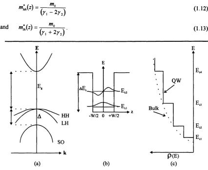
consisting of three branches near the top of the band, as shown in Figure 1.1. Each branch has two fold degeneracy due to up and down spin. The central cell character of these states is p-type. In terms of the total angular momentum states, we use the following for these states
and
Heavy - Hole states
Light - Hole states
Spin Split - Off states :
2 21
2 21
The spin split off band is depressed on the energy axis by an amount A due to the spin - orbit interaction. Due to the simplicity of the conduction band-edge, the E vs k relation near the conduction band-edge is given by a simple parabolic relation. However, the problem is more complicated for the valence band because of very strong interaction of the heavy-hole (HH) and light-hole (LH) states. Due to this interaction, the valence band becomes four-fold degenerate at the band-edge. In the Kohn-Luttinger formalism the HH and LH states are derived using a phenomenological Hamiltonian which is invariant under rotations and is constructed with the two vectors k and J as
H =
2/Wn r, + - ^ 2)*
2 /,(k .J )= (1,8)
where mo is the ffee-electron mass and y, are the Luttinger parameters. Taking the wavevector k along z-axis, the Hamiltonian (1.8) will take the form
H =
2njr y A + - r 2 - ' ^ r 2 ^ j (1.9)
where mj is projection of J along the direction of k. The two resulting eigen values for HH and LH states are then given by
h^k-and
2m,
h^k
2/w,
(y, - 2 / J for mj = ± 3/2
0
21.2
(Xi + 2^2) • for mj = ± 1/2
(1.10)
These two bands are still degenerate at k = 0, but the degeneracy is lifted at finite k
values due to the different effective hole masses
=
and ml{z) =
(y, - 2r : )
(1.12)
(1.13)
E
HH LH
SO
(a)
k
aE,
^ f
^c2
--- ► -W/2 0 +W/2
(b)
QW
X
Bulk
P(E)
(c)
Figure 1.1 : Schematic illustration of (a) band diagram of a direct-gap III-V semiconductor, (b) conduction band energy level diagram of a QW structure, and (c) a comparison of density of states function between bulk and QW system.
Typical values of Luttinger parameters for some important III-V semiconductors are given in the Table 1.1 below.
Table 1.1 : Values of the Luttinger parameters for some important III-V
semiconductors.
Material Yi Y2
GaAs 6.85 2 .1
InAs 19.67 8.37
InP 6.35 2.08
2 1.2 h^k
2m (1.14)
where Ec is the conduction bandedge and m* is the effective mass of the electrons. In general the effective mass of the carriers is given by the second derivative of the energy E, with crystal momenta p = .
1 d^E 1 d^E
(115)
dp^ ft" dk^
The effective mass for a narrow parabola at the band-edge, therefore, would be smaller in comparison to a wide parabola.
1.2.1 Envelope Function Approximation
The quantised energy levels in a QW can be calculated using Envelope Function Approximation^ (EFA). In EFA the wavefunctions of electrons confined to the QW can be written as
exp(yk^ • r„ ), (1.16)
where the subscript c (or v) and n = 1,2,— denote the conduction band (or valence
band) and the number of quantised energy levels in the well respectively. The Bloch functions, U c (r) are assumed similar in the two semiconductors constituting the well. In
(1.16), kn and rn represent the wave vector and position vector of electrons both parallel to the interface of the heterojunction and ( p c n ( z ) is the slowly varying envelope function.
The slowly varying part of the wavefimction can be obtained by solving the Schrodinger equation for one dimensional potential well
1 d
2 dz
+ F(z) (1.17)
/w*(z) dz
The eigen functions, (pen, can be calculated from (1.17) by distinguishing the effective
mass of electrons within the well and barrier by and respectively. Hence,
Cosl
Sin
n: even
or, ?>„(r) = 5exp (2m ’/ /o r (H S W /2) (1.19)
where, A and B are constants and W represents the width of the quantum well. The depth of the potential well for conduction band electrons is replaced by the band off-set AEc- Using the appropriate boundary conditions at the interfaces, that the wavefimction
( p c n ( z ) and ^lm*{z) d ç ^ld z^ should be continuous across the boundary, the energy
eigen functions for conduction band electrons can be calculated from the following equation.
% = tan
i n (1.20)
An illustration of a solution for the conduction band states is shown in Figure 1.1. The number of bound states is given by
\ + Int 2 * 2
TT^n (1.21)
showing that there is always one bound state. Taking into account discrete states along the z-direction and continuous states parallel to the interface, the total energy of electrons confined within the well can be written as
n^ E = +
2m
Àkl^K)
(1.22)For the valence band, as has been discussed in the bulk case, multiple sub-bands occur due to the quantisation of electron motion in z - direction. However, the quantum confinement o f the charge carriers in a QW system is expected to modify the band structure for the in-plane motion of the carriers, leading to a removal of band degeneracy. In a successive perturbation approach, the QW potential is treated as a first perturbation to the
k
= 0 unperturbed states which lifts the degeneracy between the mj =± 3/2 and ± 1/2 bands. The Luttinger interaction is then added as a new perturbation to the QW levels. If we insert in (1.8) the values k%= kj_, and ky = 0, the k-dispersion in a [1 0 0] direction perpendicular to the z-axis is then given by
rC~k]
and for mj = ± 1/2 (1.24)
In transverse dispersion, the heavy-hole band, therefore, has a light mass mo/(yi + 72)
whereas the light-hole band now has a heavy mass mo/(yi - 72
)-A typical valence bandstructure of 100 Â Ga)-As/)-AlGa)-As QW is shown in Figure 1.2\ It can be seen that the E vs kn relations are no longer parabolic and degeneracy between HH and LH bands is lifted at kn= 0 because of quantum confinement.
0.00
HHl
LHl
-0.02
HH2 -0.04
I
-0.06
I
HH30.08
-0.10
LH2
-0.12
0.04 0.03 0.02 0.01 0.00 0.01 0.02 0.03 0.04
<— (110) Wave Vector ( 1 /A) ( 100) —►
Figure 1.2 : Valence band structure of 100A GaAs/AlGaAs QW structure showing non-parabolicity of the bands. The HH and LH states are split due to quantum confinement at kn=0.
1.2.2 Density o f states
In a 3-dimensional system, the density of states function can be derived by dividing the k- space volume between vector k and k + dk by the k-space volume per electron state. Denoting the energy and energy interval corresponding to k and dk as E and dE, we can therefore write the following expression for the number of electron states in the conduction band between E and E + dE as
where V = L^ is the volume of the crystal. Assuming a parabolic band nature near the bandedge to substitute for k in (1.25) using the relation E = {h^k^ a n d
accounting for the spin degeneracy, the final expression for the density of states per unit volume for the conduction band electrons in a bulk semiconductor can be written as
^ rVi
P.o(E)= • (126)
TT^n-Following exactly the same procedure, the density of states function of electrons in a 2D system (QW) can be derived and is given by
P2d{E) = - ^ . (1.27)
Tin
As can be seen from the above expression, the density of states in a 2D system is constant and independent of carrier energy. In a multi sub-band system, however, the total density of states at energy E is calculated by summing over all sub-band states and as a result it varies in a step wise manner. We can express it mathematically as
°° i w *
= (1.28)
where H(x), the Heaviside function which is equal to unity when x > 0 and is zero when X < 0. The comparison of density of states between a 3D and 2D case is shown in Figure 1.1. In the 3D case, the density of states function is shown by dotted line. This modification in the density of states function in QW structures leads to some important consequences for the recombination of charge carriers, such as :
(i) The Recombination process involves electron and hole assemblies of definite energies i.e. less broadening of recombination radiation.
(iii) Enhanced electron - phonon interaction and the possibility of lasing action occurring with the participation of phonons.
(iv) The effective bandgap of the material increases by the sum of the electron and hole confinement energies.
Finally, in a 1 D system or a “quantum wire”, the density of states is given by
p ,o (£ ) = — (1. 29)
7m
We note that as the dimensionality of the system changes, the energy dependence of the density of states also changes.
1.3 Optical Transitions
of suitable momentum to satisfy the momentum conservation rule. In order for the right phonon collision to occur, an electron has to dwell in the conduction band for a longer time. Since no crystal is perfect, there are impurities and defects in the lattice that manifest themselves as traps and recombination centres. It is most likely that the electron and hole will recombine non-radiatively through such n defect center, and the excess energy is dissipated into the lattice as heat. The probability of radiative recombination in an indirect bandgap semiconductor such as Si, or Ge, is therefore greatly reduced due to competing non-radiative processes.
In an intrinsic semiconductor under thermal equilibrium the position of the Fermi level Ef
is constant throughout and it lies within the bandgap. This means that the concentration of the free carriers, both electrons and holes, are constant throughout the crystal. However, when excess carriers are generated within the semiconductor, the crystal departs from the thermal equilibrium state and as a result the Fermi level splits into quasi- Fermi levels for electrons and holes respectively. The non-equilibrium carrier concentrations may then be calculated using the following distribution functions
f=(E) = --- 7 ^ - - - O-30)
E - E,
1 + exp 'FC
V kgT j
fv(E) = --- (1.31)
1 + exp Epv - E
V kgT j
where Epc and Efv are quasi-Fermi levels for electrons and holes respectively. The
difference (Epc - Efv) is a measure of the deviation from the equilibrium state. The non equilibrium electron and hole concentrations are given by the following integrals
n=\UE)pAE)dE (1.32)
Ec
E,
where Ec and Ev are the bandedge energies of the conduction and valence band respectively. Thus, in Boltzmann approximation ( E - Ef » kgT ) under low carrier
injection, the integrals (1.32) and (1.33) yield the following expressions for non- equilibrium electron and hole densities
n - exp V k j
p = exp
k j
(1.34)
(1.35)
where Nc and Nv are constants and are called effective densities of states in the conduction and valence band respectively. It is also evident from the above expressions of the carrier densities for electrons and holes that the charge neutrality condition does not hold in non-equilibrium condition i.e.
np;^nf (1.36)
where n; is the intrinsic carrier density of the charge carriers. It is also important to note that these results will change under high injection in a semiconductor laser.
1.3.1 Band-to-Band Recombination
When excess carriers are generated in a semiconductor by means of either optical excitation or current injection, a dynamic equilibrium is established within the crystal which makes excess carrier densities of both types of charge carriers equal (An = Ap). The density of excess carriers returns to the equilibrium values after the excitation source is removed. The excess carriers decay usually following an exponential law ~ exp(-t/i), where i is defined as lifetime of excess carriers. In general, the excess carriers decay by radiative and/or non-radiative recombination as has been discussed previously. Therefore, the total lifetime x can be expressed as
- = - + — (1.37)
’’‘•T â K 'T T h r.
<■’*>
where Rr (= An/Xr) and R^r (=An/Xnr) are radiative and non-radiative recombination rates per unit volume respectively. Therefore, to achieve high internal quantum efficiency, the ratio x/Xnr should be as small as possible, or Xnr should be as large as possible.
The radiative recombination rate of electrons and holes in a semiconductor at equilibrium is given in terms of recombination constant B as
R, = Bnf = B{n„Po ) (1.39)
where n, is the intrinsic carrier concentration, the square of which is equal to the product of equilibrium concentrations of electrons and holes. The value of the recombination constant is different for different materials and chiefly depends on the band structure of the material. Direct band-gap semiconductors usually have values of B ranging from 10'" to 10'^ cm^s*^ and indirect band-gap semiconductors have values of B ranging fi"om 10'" to 10'" cm^s'\
The recombination rate of a system which has departed fi'om equilibrium is
increased by a factor npjn^ with respect to the equilibrium rate R,. and can be written as
T. ) = + p „ + A w ) ^ . (1.40)
Therefore, the carrier lifetime during the radiative recombination process may be found out from
For low injection levels, such that An < no, po
r, = when « n^ = (1.42)
or, = {b n when n^ « p^ = (1.43)
When An » no, po, the doping level no longer affects the radiative lifetime, which then depends on the excitation level according to
r , s ( 5 A « ) '. (1.44)
This is the bimolecular recombination regime, when the lifetime changes with An and this is the situation which occurs in the undoped active region of a double heterostructure (DH) laser.
1.3.1.1 Matrix Element
Photons interact with the semiconductor through electric dipole coupling to cause transitions of electrons from valence band(s) to the conduction band. The interband transition probability can be calculated using time dependent perturbation theory in which the interaction Hamiltonian takes the form Hint. = -er;.^ where Ç is the electric field vector of the light and ~er[ the dipole associated with the electron. The transition rate is given by the Fermi’s golden rule^
Wi,r = N ,.f f5 (E , - E, + t o ) (1.45)
where Mj,f is the momentum matrix element and corresponds to the initial and final electron states with energies Ei and Ef respectively. The summation is taken over all initial and final states separated by ha . Since these states form part of a continuum the summation may be replaced by an integral
w = ^ £ " K / |V ; ( £ ) û E (1.46)
where pj(E) is the joint density of states function and describes the density of e-h pairs of specific energy and momentum participating in a given optical transition by emission or absorption of photons of energy E {= hœ) .
The interband optical matrix element for a QW system can be written using (1.16) as
= - e j (1.47)
where (pcn(z) and (pvm(z) are the electron and hole envelope wave functions, kc and kv are
over localised integrals involving only Bloch functions for all individual unit cells centred at Ri, the above equation can be written as
The integral in equation (1.48) is independent of Rj and is equal to QP where Q is unit cell volume and P the usual 3-D matrix element that contains the selection rules due to band symmetries and light polarisation. In the transverse direction, perpendicular to the QW plane, the summation within the bracket, gives a null contribution unless kc = ky. Only those vertical transitions between electron and hole states are therefore allowed which have the same principal quantum number n (An = 0 selection rule).
1.3.1.2 Oscillator Strength
The oscillator strength / , describes the strength of a particular optical transition and is proportional to the number of k-states coupled to a given energy range. It is defined in terms of momentum matrix elements given by
f = = (149)
where, mo is the free electron mass and i and f are initial and final states of a given transition. In the case of bulk semiconductors, due to k-conservation in optical transitions, only very few states are coupled within a given energy range. Therefore, only a small fraction of the total electrons can participate in any particular transition. However, in contrast to the bulk semiconductor, in a QW structure the step like density of states function allows all electrons and holes in the same quantised sub-band to have same k% vector which leads to better matching of electron and hole wavefunctions and therefore “concentrates” the oscillator strength.
1.3.2 Excitonic Effects
which a free electron is transferred to the conduction band and a free hole is left in the valence band. At energies lower than the bandgap there are absorption peaks which correspond to processes in which electron and hole are bound to one another via long range Coulomb interactions. Such a mutually bound electron-hole pair leads to bound levels, the lowest of which is one exciton Rydberg (R“ ) below the continuum level and in which the electron and hole are bound to each other within an exciton Bohr radius (a«x).
Two different kinds of excitons have been postulated^. In strongly ionic crystals with low mobility and dielectric constant, as in alkali halides, excitons wavefunctions are localised and have a radius comparable with the interatomic spacing. These excitons are called the Frenkel excitons. In contrast to the Frenkel excitons, in type IV or III-V semiconductors having a large degree of covalent bonding, high mobility and large dielectric constant, excitons wavefunctions spread over many unit cells of the crystal. These excitons are called Wannier - Mott excitons.
1.3.2.1 Bulk semiconductors
Pursuing the analogy with the hydrogen atom, one can derive the expression for the bound states of exciton in bulk semiconductors as given by
where n = 1,2,3,— , = (m*) ’ + (m*) \ M = ml + ml, hk is the momentum of the
centre of mass. At k = 0 and taking the zero of energy at the top o f the valence band, Eq. (1.50) can be written as
U ex
E „ = E , - - ^ (1.51)
where the exciton Rydberg, R“ = tiR/e^ and represents the binding energy of the n =1 free exciton. Similarly, one could evaluate the ground state wave function for n =1 exciton state to be
Vu{'t) = [nal,y''^^e (1.52)
(1.53) He
In bulk GaAs with m* = 0.067m^, m* = 0.45m^ and e = 13.5, Rex = 5 meV and acx =
110 A. Clearly, such an exciton is only going to be stable at very low temperature because at higher temperature it can easily be ionised into a free electron and hole due to the small binding energy.
In bulk semiconductors, the oscillator strength per unit crystal volume is given by
(1.54)
h Ttaf
where as is the Bohr radius. The factor l/jtag implies an increase in the optical
absorption for excitons over band to band transitions. An overall increase in oscillator strength per transition is given by N/n, where N is the number of unit cells in the crystal and n the number of unit cells in the exciton volume. This represents the number of excitons that can be closely packed in the crystal.
1.3.2.2 Quantum Wells
The carrier confinement in a QW structure significantly changes many properties of this two particle state. The 2D exciton exhibits properties of a 2D hydrogen atom, which means that the binding energy may be up to four times larger than in bulk 3D case. In a real QW excitons have finite but limited spatial extent in the growth direction and the wave function is squashed into an oblate ellipsoid. This is modelled by a parameter v such that the exciton binding energy and oscillator strength can be given by
E „ = 7 ÿ (155)
( n - v )
and f oe- — (1. 56)
( n - v )
oscillator strength of excitonic states significantly. However, the binding energy is strongly well width dependent. As the well width increases the binding energy approaches the bulk value since the envelope functions become delocalised. R“ increases with decreasing well width for the opposite reason. For smaller well widths R“ drops as the envelope functions leak into the barrier. The increased oscillator strength of e-h pairs in a QW system reduces the lifetime of the excitons significantly as compared to the bulk case and well resolved exciton peaks can be observed even at room temperature in the absorption spectrum just below each step in the density of states function.
1.4 Optical Characterisation
Optical characterisation techniques make use of the “luminescence” produced by the charge carriers due to radiative recombination from excited states to the ground state. A semiconductor material can be excited in a number of ways including optical excitation, high energy electron beam excitation or by charge injection and the resulting luminescence is called photoluminescence (PL), cathodoluminescence (CL) or electroluminescence (EL) respectively. Each feature of the luminescence spectrum shows a finger-print of a definite electronic transition. The possible radiative transitions may be due to (i) recombination of fi’ee electrons and holes, (ii) recombination of electrons and holes bound to an ionised impurity, (iii) recombination of fi-ee-excitons or (iv) bound- exciton recombination when excitons become localised in the vicinity of an impurity. The luminescence associated with the processes (i) and (iii) is called intrinsic luminescence
PL and CL both have been frequently used in this project for the assessment of material quality and growth dynamics on patterned substrates. A brief detail of the principle and application of these techniques is given here.
1.4.1 Photoluminescence (PL)
Photoluminescence (PL) , with its ability to identify impurities and defects, is the most widely used optical method for material characterisation in both cases of bulk semiconductors and low dimensional structures. In a typical PL experiment, luminescence is excited in the sample by absorbing photons from a laser, usually in the barrier layer of a QW, creating electron-hole pairs. The electron and hole are then readily captured by the well as hot particles, but rapidly thermalises down to the lowest available energy configuration via emission of LO phonons. At low temperatures and relatively low excitation densities, these electrons and holes bind themselves to form excitons, with a further lowering of energy, which subsequently decay giving rise to free-exciton luminescence^. Therefore, intrinsic luminescence due to free-exciton recombination dominates in the PL spectra. The energy of the photon emitted when a free-exciton collapses radiatively is
h o ) ^ E ^ - R ^ (1.57)
where R“ is the binding energy of the n = 1 free-exciton. As discussed earlier, if the material contains donors and acceptors with concentrations > 10*^ cm'^ then at low temperature virtually all of the free-excitons are captured, giving rise to impurity specific bound-exciton luminescence. Bound-exciton luminescence lines are very sharp with photon energy given by
hû) = E ^ - R ^ - E ^ ^ . (1.58)
The spectral lines associated with bound-exciton decay are observed at energy Ebe below
the excitonic ei-hhi intrinsic luminescence, where E b e is the binding energy of the exciton
to the impurity^. A blue shift in the absorption spectrum relative to the emission spectrum at low temperatures is characteristics of bound-excitons. For bulk semiconductors, E b e is
whereas those associated with the acceptors lie between 27 to 35 meV above the valence band maxima. The binding energy of excitons bound to donors is therefore expected to be less than that for acceptors. In a QW structure, the binding energy depends both on the well width and position of the impurity within the well*.
radiative lifetime of the carriers*^. The increase in the radiative lifetime of the carriers with temperature results in a decrease of the luminescence efficiency, as given by Eq. (1.38). Moreover, at high temperatures excitons dissociate into fi’ee carriers and band-to- band recombination dominates.
Excitonic luminescence in QW heterostructures is very sensitive to spatial and chemical variations within and close to the quantum well. The full width at half maximum (FWHM) of the PL peak is generally considered as a measure of the layer or interface quality. However, many factors contribute to the FWHM of the PL spectrum and great care must be taken in interpreting the PL emission. Here, we will discuss briefly a few of the important parameters which can significantly affect the QW emission.
1.4.1.1 Effect of Well Width Fluctuations.
Fluctuations in the well width change the confinement energy of the exciton and, hence, the FWHM of the PL spectrum. In an infinite deep well approximation, the confinement energy of a carrier is proportional to the square of the reciprocal of well width d (E oc 1/d^). An uncertainty of Ad in the well width will, therefore, cause an uncertainty in the
energy AE ( oc Ad/d^). Though, the infinite deep well approximation does not apply to a
1.4.1.2 Effect of Alloy Fluctuations.
The exciton wave function is never wholly confined to the quantum well and a part of the wave function penetrates into the barrier regions. The random compositional variations in the QW inevitably causes random variations in transition energy. The influence of such fluctuations on PL line width depend on what fraction of the exciton wave function penetrates into the barrier regions*^. Then it becomes obvious to think that in quantum wells with ternary barriers, for example GaAs/AlGaAs systems, alloy broadening would be most severe for narrow wells as the exciton wave function samples a larger volume of the barrier region On the other hand, for InGaAs/GaAs system the effect of alloy broadening should be more severe for wide wells.
Though PL spectra can provide a great deal of information about material quality and concentration of defects or impurity levels, it does not give complete information about the composition and width of the active region in a QW structure. A knowledge of emission and absorption spectra together, on the other hand, can provide a more detailed understanding of the quantum well material*^.
1.4.2 Photoluminescence Excitation ( PLE )
important feature of PLE which shows its ability to measure all of the inter sub-bands transition energies in contrast to the ground state data provided by conventional PL. Knowing the positions of the first two sub-band transitions fi'om the PLE spectra of a QW structure, it is then possible to determine the well width and its composition by fitting the data to a finite well model.
1.4.3 Time Resolved Photoluminescence ( TRPL )
Due to the increasing application potential of QW heterostructures for the development of high speed photonic devices, a proper understanding of carrier dynamics in these structures is very important. Time resolved photoluminescence spectroscopy is a standard technique employed for PL decay measurements in QW structures. The radiative life time, Xr, of carriers in QW structures is found to be an order of magnitude shorter than those observed in bulk material of comparable quality. Therefore, the gain g, which is proportional to the spontaneous radiative life time x , , should be improved by the same factor in QW lasers causing, in turn, a reduction in the threshold current*^. The reduced radiative life time of the carriers in 2D structures is explained due to the enhanced overlap of electron and hole wavefunctions resulting an increase in oscillator strength in these structures. The carrier lifetime and the recombination dynamics, however, depend also on the quality of hetero-interfaces and the impurity contents in the well and adjacent barrier layers. Therefore, it is a sensitive probe of the quality of the quantum well material.
1.4.4 Cathodoluminescence ( CL )
Cathodoluminescence (CL) is a particular mode of operation of the scanning electron microscopy (SEM), which provides measurements with high spatial resolution for microcharacterisation of semiconductors. Cathodoluminescence as the name suggests is the emission of light as a result of electrons (‘cathode ray’) bombardment. Both PL and CL provide much the same information about the energy states of the sample, however, in the case of CL the energy dissipation volume (^ 1 pm^) is orders of magnitude smaller than that corresponding to PL Therefore, the intensity of the luminescence signal is low in CL as compared to PL However, an important advantage of CL, in addition to the high spatial resolution, is its ability to obtain more detailed depth - resolved information by varying the electron-beam energy*^.
R = - V ; (1-59)
where p is the density of the material, k depends on the atomic number of the material and is also a function of energy and a depends on the atomic number and electron beam energy. For the electron beam energy range of 5 - 25 keV and atomic numbers 10 < Z <
15, Everhart and Hoff^ calculated the penetration range to be
(1.60)
V p ;
where p is in g/cm^ and Eb is in keV.
CL is more suited for layer characterisation grown on patterned substrates as its high spatial resolution allows a direct comparison of the relative luminescence efficiency of small regions (such as ridge top) as well as mapping of the emission wavelength as a function of distance from the ridge side walls.
1.5 Optical Devices
The ability to fabricate quantum well structures with very smooth interfaces, has given rise to the invention of many optical devices with superior performance in standard applications or with new functionalities. Quantum confinement of charge carriers in these structures greatly modifies their optical properties which leads to many interesting applications in the field of optoelectronics. In this section, we discuss briefly a few of the important properties of these quantum well devices, particularly lasers, modulators and segmented contact devices which allow integration of multifunctional components on a single substrates.
1.5.1 Quantum Well Lasers
formed and, under forward bias conditions, electrons and holes move towards the active region where they recombine radiatively, giving rise to photons of energy equal to the bandgap of the active region. However, these photons can also be absorbed through a reverse process that generates electron-hole pairs. When the current through the junction exceeds a critical value, a condition known as population inversion is achieved in which the rate of photon emission exceeds that of absorption resulting in stimulated emission
in which the emitted photon has exactly the same energy and momentum as the incident photon The semiconductor material is then able to amplify the electromagnetic radiation and is said to exhibit optical gain. A Fabry-Perot (FP) cavity is formed by the cleaved facets of the semiconductor material which provides the optical feed back to build up the necessary photon density within the cavity for stimulated emission. The optical feed back is strongest for those wavelengths of electromagnetic radiation which correspond to one of the longitudinal modes of the cavity.
Electrons
r r
(A lG aA s Top
contact E,
(AlGaAs) p-AIGaAs
GaAs n-A lG aA s Bottom contact
Figure 1.3 : Schematic of (a) a GaAs/AlGaAs DH laser, (b) corresponding band diagram and spatial mode profile of the emitted light.
quantum-mechanical effects are expected to occur. As a consequence, motion of the carriers perpendicular to the growth plane gets quantised giving rise to discrete energy levels and leading to a step like density of states function. A QW laser therefore has a larger density of states near the bandedge and so it is harder to achieve inversion as compared to a DH laser. However, for the same reason the gain in a QW laser is much greater than a DH laser. Therefore, for the same gain threshold current is much smaller in a QW laser as compared to a DH laser.
The medium gain gü, at threshold in a FP cavity is obtained by applying the condition for self sustained oscillations, which states that the optical wave intensity after a round trip in the cavity must be equal to its initial amplitude^V This is conveniently written as
IqRiR; exp[(rgu, - a J2L] = I, (1.61)
where T is the optical confinement factor representing the fraction of the light confined into the active region. The total internal loss coefficient a, used in Eq.(1.61) includes all sources of loss and in more general terms it can be written as
“ i = T a .+ ( l- r ) a ,+ a „ „ (1.62)
where a , is the loss term in the active region mainly associated with free carrier absorption, etc, represents losses in claddings on both side of the active layer and Ogcat. is the scattering loss at heterostructure interfaces. Eq. (1.61) can be rewritten in the form
r g . = a . + ^ l n ^ (1.63)
In QW lasers with very thin active layer, F can become very small (F oc W^). As a result, the optical wave is less confined in the active layer and most of the wave function leaks into the barrier regions. The confinement factor can be significantly increased using the separate confinement heterostructures (SCH) scheme. In SCH, the optical confinement is provided separately by a set of optical confining layers on either side of the QW while the carrier confinement still occurs in the well.
1.5.1.1 Gain and Threshold Current Density
g ( E ) = . fM V i( E X n ( E ) - f.( E - E .)) d E (1.64)
where n, is the refractive index, M is the interband matrix element, p,(E) is the joint density of states of conduction and valence band states separated by the transition energy Et ( = E1-E2 = hv ). For a given current injection, ^(E) and fv(E) are the values of the
Fermi - Dirac distribution functions in the conduction and valence bands, respectively. Equation (1.64) can be written in a more simple form as^
g(E) = a „ ( E X f ,( E ) - f ,( E - E .) ) (1.65)
where Oo(E) is the absorption loss of the unpumped medium. In non-degenerate semiconductors under equilibrium, the Fermi level lies within the bandgap with ^ = 0 and fv = 1, the gain is negative and material is lossy due to absorption. In the case of a fully inverted system fc = 1, fv = 0, the gain is equal to the loss. Therefore, in order to achieve net gain, the material need to be pumped such that f g ( E ) - f y ( E - E j ) 0 . This is the
Bernard - Durrafourg condition^. Substituting the relevant expressions for fè and fv, this can be expressed in terms quasi-Fermi levels for electrons in the conduction band and for holes in the valence band as
Epc - E p v >Ej. (1.66)
states function, there is larger number of carriers at the sub-band edge which contribute to the gain at its peak Therefore, the spectral gain curve has a steeper slope in case of 2D as compared to 3D case. However, the gain saturates at a given finite value when the electron and hole states are fully inverted, whereas gmax never saturates in 3D due to filling of an ever increasing density of states. The peak gain, gmax, almost varies linearly with injected carrier density and can be written as
8m« = g = A ( J - J o ) (1.67)
where A is the differential gain and Jo is called transparency current density.
E=E ,-Ej=hv
g
E
n
>E
n
(a) (b) (c)
Figure 1.4 : Graphical presentation of (a) Bernard - Durrafourg condition for stimulated emission, (b) build up of gain in a DH laser (top) and in a QW laser (bottom), and (c) variation of peak gain as a function of injected carrier density in a DH (top) and QW (bottom) lasers.
Combining Eqs. (1.63) and (1.67) an expression for the threshold current density can be deduced, which is given by
1
a . + ^ l n
VR1R2/
(1.68)
the width of the active region. However, below a critical thickness (about 1000 A for GaAs), the last term in (1.68) increases dramatically as the confinement factor diminishes very fast due to its quadratic dependence in comparison to slight increase in the differential gain. As a result the threshold current density increases. As discussed earlier in section 1.5.1, the confinement factor F can be optimised in QW lasers, using the separate confinement heterostructure scheme, and can be made independent of active layer thickness. However, for very thin wells the quantised energy levels within the well are pushed up and some carriers may spill over into the optical confining layers resulting in an increase in the threshold current density. Therefore, minimising the threshold current density in QW lasers require optimisation of various design parameters. Use of graded index separate confinement heterostructures (GRIN-SCH), where the composition of the optical confining layers is graded between low and high levels, increases the carrier capture efficiency within the well which has a favourable effect on the threshold current density.
Owing to the gain saturation effect in QW lasers, due to the step like density of states, there exists an optimum number of QWs for minimising the threshold current for a given total loss atoui- In a multiple quantum well (MQW) laser consisting of N wells, assuming the carrier density in each well is constant, the modal gain Fg* can be increased by N times the modal gain of a SQW laser^'*. Consequently the gain saturation effect can be avoided by increasing the number of wells although the injected current to achieve this gain also increases by the same factor. The choice of using a MQW or a SQW laser depends very much on the total loss within the system. For a low loss system the use of SQWs will require minimum injection current to achieve the necessary gain. Whereas for high loss system, the use of MQW is preferable because the gain stems fi’om the steeper part of the gain - current curve instead of saturated part of the SQW gain curve.
1.5.1.2 Effects of Strain
conduction band mass and m* is the heavy valence band mass. Due to asymmetry in the effective masses of the electron and hole, the density of states is much greater in the valence band than that in the conduction band. When the carrier injection level is increased, the quasi-Fermi level for electrons, E f c , moves much faster into the
conduction band, even before the quasi-Fermi level for holes, E f v , has reached the
valence band edge This requires, roughly, more than double the injection level for achieving transparency in comparison to the ideal situation of equal density of states in conduction and valence bands. This situation is even worse in case of the bulk semiconductors where the ratio of density of states function is proportional to
If a thin layer of a semiconductor with different lattice constant than the substrate is grown then the lattice mismatch is accommodated by the tetragonal distortion of the overgrown layer producing built in strain in the system. For example, when a layer of a semiconductor with lattice constant larger than the substrate material is grown, the layer is compressed in the growth plane and relaxes by expanding along the growth direction. As long as the thickness of the mismatch epilayer is below a critical thickness, the strain produced is uniform and no misfit dislocation are produced. In III-V semiconductors, this built-in strain destroys the cubic symmetry of the lattice and removes the degeneracy of heavy-hole and light-hole bands. An important consequence of this splitting is that the effective mass of holes, and hence the density of states at the valence band-edge decreases dramatically as a function of strain The reduced hole mass allows the inversion condition to be reached at a lower injection density. This effect was originally proposed by Adams^^ who pointed out three main advantages, reduced current density to achieve inversion, reduced intervalence band absorption, and reduced Auger recombination, respectively, due to valence band modification by growing a strained layer of InGaAsP on GaAs. Yablonovitch and Kane^^ have demonstrated, by their numerical calculations, a considerable reduction in the valence band effective mass in the plane of the active layer, under biaxial compression, and have predicted threshold current density as low as 10.0 A/cm^ under ideal circumstances.
maxima. Under biaxial compression, the upper valence band has the heavy-hole character along the growth direction, ki, whereas, it has comparatively light-hole character parallel to the growth plane, kn. However, the nature of splitting is reversed for tensile strain. The effect of strain on band structure of a III-V semiconductor is shown in Figure 1.5^^. It is the in-plane effective mass of the hole which determines the density of states and hence, optical gain and threshold current density whereas the effective mass along the growth direction determines the confinement energy in a strained quantum well heterostructure. The hydrostatic component does not change the symmetry of valence band states. Its main effect is to change the overall bandgap. The combined effect of both components of strain can be written in terms of the hydrostatic deformation potential a and the tetragonal shear deformation potential b as^*
AEy, = - 2 a s
c „ + be
- be
^ C „ + 2 C „ ^ C„
C,, + 2C,2 Cn
(1.69)
(1.70)
where AEhh and AEu, represent the shift in the heavy - hole and light - hole valence band edge with respect to the conduction band edge respectively, Cÿ are elastic coefficients, and the strain is given by
Aa.
e = ± (1.71)
where ao is the lattice constant of the substrate material. The sign in Eq.(1.71) is chosen to be positive for biaxial compression and negative for biaxial tension.
Another important effect of introducing strain in semiconductor lasers is control over polarisation of the emitted light^^. Emitted light is TE or TM polarised depending on whether the electron combines with heavy or light-hole. Valence band states are four fold degenerate at the band maxima and are described by Eqs.(l.S) and (1.6) in section 1.2. Electrons recombining with y-like and z-like valence states contribute to TE and TM gain, respectively while electrons recombining with x-like states contribute only to spontaneous emission. Averaging over all the states results in equal contributions to light polarised along the three directions. However, in a strained layer structure, this four fold degeneracy is broken and ±3/2 states dominate recombination under biaxial compression, while ±1/2 states dominate recombination under biaxial tension. The ±3/2 states have no z-like component so that TE gain will be enhanced relative to TM gain under compressive strain. Conversely, ±1/2 states have 2/3 z-like character so that TM gain will be enhanced under tensile strain.
CB
I
SO
r
K
CB
SO
r
Hl(a) (b)