© 2018 IJSRST | Volume 4 | Issue 2 | Print ISSN: 2395-6011 | Online ISSN: 2395-602X Themed Section: Science and Technology
An Efficient Reversible PLA Implemented In BIST for More Fault Coverage
K. Jhansi1, Dr. G. N. Kodanda Ramaiah2, R. Naresh Naik3
1M. Tech, Kuppam Engineering College, Kuppam, Chittoor Dist, Andhra Pradesh, India 2Professor & HOD, Kuppam Engineering College, Kuppam, Chittoor Dist, Andhra Pradesh, India 3Assistant Professor, Kuppam Engineering College, Kuppam, Chittoor Dist, Andhra Pradesh, India
ABSTRACT
Reversible logics are one of the most vital logics in present and it has different areas for its application ,those are low power CMOS, quantum computing, nano technology,digital signal processing etc., Logic synthesis for reversible logic differs considerably from standard logic synthesis. Reversible logic has been motivated by consideration of zero-energy computation thus it reduces the power utilization. A programmable logic array (PLA) is a kind of programmable logic device used to implement combinational logic circuits,Re- conFigure urability and structural regularity of Programmable Logic Devices caused wide use of it by the logic designers. Here in this paper we propose a design algorithm for a PLA with a newly designed low cost 3×3 reversible NMG circuit for implementing multi-output ESOP (Exclusive-OR Sum of Product) functions. In addition to this work is to make the design efficient reversible PLA implemented in built in self test (BIST) to enhancing the testing properties like power, fault coverage. The total work has been implemented in Xilinx 14.3 tool using verilog code.
Keywords : Reversible Logics, PLA, ESOP, BIST.
I.
INTRODUCTION
Reversible computing has emerged as a possible low cost alternative to conventional computing in terms of speed, power consumption, and computing capability. According to Landauer [1] in 1961, every operation performed by a conventional computer dissipates at least kTln2 amount of energy for every erasure of bits,wherek is theBoltzmann constant and T is the temperature where computation is performed. Reversible circuits are capable to provide less or almost zero heat dissipation [2]. With providing low power VLSI designs, this sort of computing has interesting applications in various areas including quantum computing [5], nanotechnology, cryptography, bioinformatics etc.
Reversible computing is the application principle of recycling to the computing. It is based on the fact that
input can be reconstructed from output. Like conventional circuits, the reversible circuits should also be protected from faults. Depending on their detection time, these approaches have been categorized into offline and online. This paper extends an existing PLA which is made of AND array logic and OR array logic thus provides output as Sum of Products (SOP) by Reversible PLA made ofNMG (new mux gate) gate which provides output as ESOP (Exclusive-OR Sum of Product) approach and extended by testable substitution of this PLA in Built in Self Testto enhancing the testing properties like power, fault coverage.
and Its Procedure. In Section 5 the simulation results are shown and last of all this paper is concluded in section 6.
II.
REVERSIBLE LOGICS AND
PROGRAMMABLE LOGIC ARRAY
In this section, basic definitions and ideas related toReversible Logic and Programmable Logic Array are presented with Figure s
2.1 REVERSABLE LOGICS
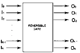
Reversible Gates are the circuits in which number of outputs is equal to the number of inputs and there is a one to one mapping between the vector of inputs and outputs.It helps to determine the outputs from the inputs as well as helps to uniquely recover the inputs from the outputs. The general structure of a reversible gate is shown in Figure 1
Figure 1. A n × n Reversible Gate
2.1.1Constant Inputs
This alludes to the quantity of data sources that are to be kept up steady at either 0 or 1 keeping in mind the end goal to incorporate the given sensible capacity.
2.1.2Garbage Outputs
Garbage Outputs indicates the number of outputs which are not used in the synthesis of a given function. In certain cases these become mandatory to attain reversibility. Therefore garbage is the number of outputs added to make an n-input k-output
2.1.3Quantum Cost:
Quantum cost may be defined as the cost of the circuit in terms of the cost of a primitive gate. It is calculated by the number of primitive reversible logic gates (1*1 or 2*2) required to realize the circuit. The quantum cost of a circuit is the minimum number of 2*2 unitary gates to represent the circuit keeping the output unchanged. The quantum cost of a 1*1 gate is 0 and that of any 2*2 gate is the same, which is 1.
2.1.4Basic Reversible logic gates:
Some of the important reversible logic gates are: NOT Gate, Feynman Gate, Toffoli Gate, Fredkin Gate and Peres gate as give below
NOT Gate:
The simplest Reversible gate is NOT gate and is a 1*1 gate. The Reversible 1*1 gate is NOT Gate with zero Quantum Cost is as shown in the Figure 2.
Figure 2. NOT Gate
Feynman Gate:
Figure 3 shows The Feynman gate which is a 2*2 gate and is also called as Controlled NOT and it is widely used for fan-out purposes. The inputs (A, B) and outputs P=A, Q= A XOR B. It has quantum cost one
Figure 3. Feynman Gate
Double Feynman Gate:
is O (P, Q, R). The outputs are defined by P=A, Q=A⨁B, R=A⨁C.
Figure 4. Double Feynman Gate
Toffoli Gate:
Figure 5 shows a 3*3 Toffoli gate. The input vector is I (A, B, C) and the output vector is O(P, Q, R). The outputs are defined by P=A, Q=B, R=AB XOR C Quantum cost of a Toffoli gate is 5
Figure .5 Toffoli Gate
Fredkin Gate:
Figure 6 shows a 3*3 Fredkin gate. The input vector is I (A, B, C) and the output vector is O (P, Q, R). The outputs are defined by P=A, Q=A′BAC and R=A′C AB. Quantum cost of a Fredkin gate is 5
Figure 6. Fredkin Gate Peres Gate:
Figure 7 shows a 3*3 Peres gate. The input vector is I (A, B, C) and the output vector is O (P, Q, R). The outputs are defined by P = A, Q = AB, R=ABC. Quantum cost of a Peres gate is 4
Figure 7 Peres Gate 2.2 PROGRAMMABLE LOGIC ARRAY
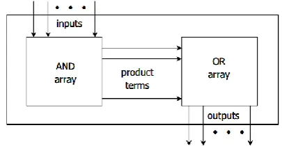
Programmable Logic Array is a programmable gadget used to execute combinational rationale circuits. The PLA has an arrangement of programmable AND planes, which connect to an arrangement of programmable OR planes, which would then be able to be restrictively supplemented to deliver an output in Sum of Products (SOP) form. This design takes into consideration a substantial number of rational capacities to be blended in the total of items standard structures.
A Programmable Array Logic Array (PLA)consists of two planes, the first one isprogrammable AND plane and the second one isprogrammable OR plane which is all togetherknown as AND-OR PLA. The architecture of PLA is shown in Figure 8
Figure 8. Architecture of Programmable Logic Array
Figure 9. Example of PLA 2.2.1ESOP PLA:
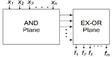
PLAconsists of two planes, the first one is programmable AND plane and the second one is programmable OR plane which is all together known as AND-OR PLA. When the second plane works as Ex-OR, then it is called AND Ex- OR PLA and the Output of this PLA is to be in the form of Exclusive-OR Sum of Products (ESOP). The Architecture of ESOP PLA is shown in Figure 10
Figure 10. AND-EXOR Programmable Logic Arrays
III.
EXISTING REVERSIBLE PROGRAMMABLE
LOGIC ARRAY
A Programmable Array Logic Array (PLA)consists of two planes, the first one isprogrammable AND plane and the second one isprogrammable OR plane which are made by using Reversible Logics called as Reversible PLA.
The architecture of Reversible PLA is shown in Figure 11
Figure 11. Reversible PLA
The design of Reversible PLA was first proposed in[11], which has used Feynman and Toffoli gates to realizeReversible PLA for multi-output ESOP operation whereToffoli gate is used for AND operation and Feynman gateis used for Ex-OR operation. In [12] Fredkin gate is used in AND plane of reversible PLA for AND operation which costs 5 for each gate resulting higher quantum cost.
3.1 Proposed Reversible gate:
A 3×3 reversible gate namely New Mux (NMG)Gate is proposed which is drawn in Figure .12. The NMG gate can be defined as Iv = (A, B, C) and Ov = ((P = A⊕B),(Q= B’C⊕AC’),( R= BC⊕ AC’)), Where Iv and Ov are the input and outputvectors respectively. The corresponding truth table of theNMG gate is shown in TABLE 1.
It can be verifiedfrom the truth table that the input patterncorresponding to a particular output pattern can beuniquely determined.
3.2 Design of Reversible Programmable Logic Array(RPLA):
In this structure, we will synthesize the multiple-output ESOP functions using different conFigure urations of NMG gates.
Figure 13. Different modes of operation of (a), (b) & (c) Feynmandouble gate, (d). Feynman gate and (e) &
(f).NMG gate
In multi-output ESOP, some products may becommon among different output functions. We will alsotake the advantage of those terms like as irreversible PLA.The main constraint is that the fan-out of all signals in areversible gate is one.In the synthesismethod for multi-output ESOP using the RPLA, it isassumed that the multi-output circuit has been alreadyminimized and is available in an ESOP format. Forconvenience we will denote different modes of operationof NMG, Feynman and Feynman Double gate as shown inFigure . 13.
Example 1: Consider the following ESOP functions:
F1= AB’C⊕A’B F2= A’B’C⊕AC F3 = AB’C⊕BC’⊕A’B F4 = AC
F5 = BC’⊕A’B⊕AC
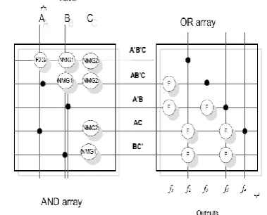
We constructed Reversible PLA circuit of example 1 taken above. Such that For the multi-output function given in Example1, the frequency of A’Bis 3 as it is shared among theoutput functions F1, F3, F5; whereas the frequency of
A’B’Cis one, as it is shared only by F2.Table II shows thefrequency of each product terms for Example 1.
TABLE 2. Frequency Table for the ESOP Given In Example 1
The Feynman Double gates in AND plane are used tocopy the input variables and their complement which removes the fan-out problems. Whereas, the NMG gatesare used for AND operations. The realization of AND plane generatesthe order of Productsand EX-ORplane will be constructed according to Feynman gate properties. The realizationof the proposed reversible PLA is shown in Figure 14.
IV.
PROPOSED BUILT IN SELF TEST (BIST)
AND ITS PROCEDURE
After the implementation of Reversible PLA it is used in the Built in self test such that the implementation of the built in self test with PLA is shown below
4.1 Built In Self Test:
A built-in self-test (BIST) or built-in test (BIT) is a mechanism that permits a machine to test itself. Engineers design BISTs to meet requirements such as:
• High reliability
• Lower repair cycle times
Built-In-Self-Test is used to make faster, less-expensive integrated circuit manufacturing tests. The IC has a function that verifies all or a portion of the internal functionality of the IC. In some cases, this is valuable to customers, as well.
4.1.1 Basic Architecture:
As equipments are replaced by circuitry, so it is obvious that compressed implementations of test pattern generator and response analyzer are to be designed. The basic architecture of BIST is shown in Figure 15
Figure 15. BIST Architecture
A typical BIST architecture consists of
• TPG - Test Pattern Generator
• TRA – Test Response Analyzer (comparator) TPG can generate test patterns for CUT. It will be dedicated circuit or a micro processor. Patterns generated may be pseudo random numbers or deterministic sequence. Here we are using a Low Power Linear Feedback Shift Register (LP-LFSR) for generating random numbers.CUT is the circuit or chip in which we are going to apply BIST for testing stuck at zero or stuck at one error.
TRA will check the output of CUTand verify it with the pre defined functions having Output of LFSR as input & give the result as error or not. ROM is used to generate the predefined functions and a multiplexer is used in between the TPG and CUT which can select the input of CUT as Test patterns or normal input.
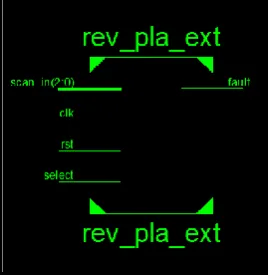
4.2 Implementation of Reversible PLA in BIST Reversible PLA is used in The BIST to test the PLA for Faults such That the Testing time will be reduced in BIST and Utilizes less power compared to other testing procedures. The fault coverage of BIST is high so that Testing of PLA is more effective.
The Reversible PLA is placed in the place of Circuit under test and the input to this PLA is from multiplexer such that it can feed the input from TPG or Conventional input which is given as input to TPG. And a comparator can compare the result from CUT and conventional results from conventional design with TPG outputs as inputs and then provides output as the CUT is faulty or not.
V.
SIMULATION RESULTS
Figure 17. Block diagram
Figure 18. RTL Schematic
Figure 19. Power Report
Figure 20. Simulation Results
VI.
CONCLUSION
In this paper, compact structure of Reversible Programmable Logic Array (RPLA) is presented. A reversible gate with low cost is proposed to generate the AND terms of RPLA. Using this property we can
ensure the reduction of gate count. The design proposed for RPLA that can realize any multi-output ESOP (Exclusive-OR Sum of Product) function. In addition, simulation of the proposed gate has shown that it works correctly. In embedded circuits and other technologies for making low power consumption, reversible PLAs are useful and This Reversible PLA can be tested by using Built in self Test Such That the power utilization will be reduced during the test.
VII.
REFERENCES
[1]. R. Landauer,"Irreversibility and heat generation in the computing process." IBM J. Res. Dev., vol.5,no. 3, pp. 183-191, 1961.
[2]. C.H. Bennett,"Logical reversibility of computation". IBM J. Res. Dev. vol.17, no. 6, pp. 525-532, 1973.
[3]. G.Schrom and S.Selberherr .Ultra-low-power cmos technology .In Semiconductor Conf, Romania, 2002. E. Knill, R. Laamme, and G. J. Milburn .A scheme foreseen quantum computation with linear optics. Nature, 409:46– 52, January 2001.
[4]. M.A .Nielsen and I.L. Chuang .Quantum computation and quantum information, 2001. [5]. R. C. Merkle. Two types of mechanical
reversible logic. Nanotechnology, 4(2):114–131, January 1993.
[6]. H .Fleisher and L. I. Maissel .An introduction to array logic. IBM J .of Research and Development, 19, 1975.
[8]. A. Mishchenko and M. Perkowski .Logic synthesis of reversible wave cascades. In International Workshop on Logic Synthesis, pages 197–202, June 2002.
[9]. M. Perkowski, A. B. P. Kerntof and et al. Regularity and symmetry as a base of efficient realization of reversible logic circuits. In International Workshop on Logic Synthesis, pages 245–252, June 2001.
[10]. D. Maslov and G. Dueck. Reversible cascades with minimal garbage. IEEE Transactions on CAD, 23(11):1497–1509, November 2004. [11]. A .R. Chowdhury, R. Nazmul, and H. M.
H.Babu."A new approach to synthesize multiple-output functions using reversible programmable logic arrays" In IEEE 19rd International Conf. on VLSI Design, pages 311– 316, Hyderabad, India, 2006
[12]. R. Rahman, L. Jamal and H.M.H. Babu, "Design of Reversible Fault Tolerant Programmable Logic Arrays with Vector Orientation", Interna-tional Journal of Information and Communication Technology Research, pp. 337-342, 2011
[13]. S.K. Mitra, L. Jamal, Mineo Kaneko and H.M.H. Babu,"Design and Minimization of Reversible Programmable Logic Arrays", Proc. of Symposium on VLSI,GLSVLSI’12, NY, USA, pp. 215-220, 2012.
[14]. Robert Treuer, Vinod K. Agarwal, Hideo Fujiwara "A New Built-In Self-Test Design for PLA's with Hligh Fault Coverage and Low Overhead"IEEE Transactions on ComputersVolume 36 Issue 3