-Nx586™ Processor
Databook
PRELIMINARY December 6, 1994
NexGen,
Incorporated 1623 Buckeye DriveMilpitas, CA 95035
Copyright © 1993, 1994 by NexGen, Inc.
The goal of this databook is to enable our customers to make informed purchase decisions and to design systems around our described products. Every effort is made to provide accurate information in support of these goals. However, representations made by this databook are not intended to describe the internal logic and physical design. Wherever product internals are discussed, the information should be construed as conceptual in nature. No presumptions should be made about the internal design based on this document. Information about the internal design of NexGen products is provided via nondisclosure agreement ("NDA") on a need to know basis.
The material in this document is for information only and is subject to change without notice. NexGen reserves the right to make changes in the product specification and design without reservation and without notice to its users. THIS DOCUMENT DOES NOT CONSTITUTE A WARRANTY OF ANY KIND WITH RESPECT TO THE NEXGEN INC. PRODUCTS, AND NEXGEN INC. SHALL NOT BE LIABLE FOR ANY ERRORS THAT APPEAR IN THIS DOCUMENT.
All purchases of NexGen products shall be subject to NexGen's standard terms and conditions of sale. THE WARRANTIES AND REMEDIES EXPRESSLY SET FORTH IN SUCH TERMS AND CONDITIONS SHALL BE THE SOLE WARRANTIES AND THE BUYER'S SOLE AND EXCLUSIVE REMEDIES, AND NEXGEN INC. SPECIFICALLY DISCLAIMS ANY AND ALL OTHER WARRANTIES, WHETHER EXPRESS, IMPLIED OR STATUTORY, INCLUDING THE IMPLIED WARRANTIES OF FITNESS FOR A PARTICULAR PURPOSE, AGAINST INFRINGEMENT AND OF MERCHANTABILITY. No person is authorized to make any other warranty or representation concerning the performance of the NexGen products. In particular, NexGen's products are not specifically designed, manufactured or intended for sale as components for the planning, design, construction, maintenance, operation or use of any nuclear facility or other ultra-hazardous activity, and neither NexGen nor its suppliers shall have any liability with respect to such use.
Trademark Acknowledgments
NexGen, Nx586, RISC86, NexBus, NxPCI, NxMC and NxVL are trademarks of NexGen, Inc.
IBM, PC AT, and PS/2 are registered trademarks of International Business Machines, Inc. Tri-state is a registered trademark of National Semiconductor Corporation. VESA and VL-Bus are a trademark of Video Electronics Standards Association.
Restricted Rights and Limitations
NexGen
ContentsContents
Preface ... v
Notation ... v
Related Publications ... vii
The Nx586 ProcessorFeatures ... 1
Nx586 Processor with Floating-Point Execution Unit Features ... 2
Nx586 Signals ... 4
NxS86 Pinouts by Signal Names ... 6
NxS86 Pinouts by PGA Pin Numbers ... 9
NxS86 Pinouts by JEDEC Pin Numbers ... 11
NxS86 NexBuslNexBusS Signals ... 17
NexBuslNexBusS Arbitration ... 17
NexBuslNexBusS Cycle Control. ... 19
NexBus Cache Control ... 21
NexBus Transceivers ... 23
NexBuslNexBusS Address and Data ... 24
NxS86 L2 Cache Signals ... 29
NxS86 System Signals ... 30
NxS86 Clocks ... 30
NxS86 Interrupts and Reset ... 32
NxS86 Test and Reserved Signals ... 33
NxS86 Alphabetical Signal Summary ... 34
Hardware Architecture ... 41
Bus Structure ... 41
Processor Bus ... 42
L2 Cache Bus ... 4S Internal 64-bit Execution Unit Bus ... .4S Operating Frequencies ... · ... 46
Internal Architecture ... 47
Contents
NexGen
Storage Hierarchy ... 48
Transaction Ordering ... 51
Cache and Memory Subsystem ... 52
Characteristics ... 52
Level-2 Cache Power-on RESET Configurations ... 53
Cache Coherency ... 54
State Transitions ... 55
Invalid State ... 57
Shared State ... 58
Exclusive State ... 58
Modified State ... 59
Interrupts ... 59
Clock Generation ... 60
Bus Operations ... 61
Level-2 Asynchronous SRAM Accesses ... 61
Level-2 Synchronous SRAM Accesses ... 63
NexBus and NexBus5 Arbitration and Address Phase ... 64
NexBus Basic Operations ... 64
NexBus5 Single-Qword Memory Operations ... 66
NexBus5 Cache Line Memory Operations ... 71
NexBus5 110 Operations ... 71
NexBus5 Interrupt-Acknowledge Sequence ... 71
NexBus5 Halt and Shutdown Operations ... 72
Obtaining Exclusive Use Of Cache Blocks ... 73
NexBus5 Intervenor Operations ... 74
Modified Cache-Block Hit During Single-Qword Operations ... 74
Modified Cache-Block Hit During Four-Qword (Block) Operations ... 75
Electrical Data ... 77
Mechanical Data ... 79
Glossary ... 83
Index ... 89
ii Nx5861M
NexGen
FiguresFigures
Figure 1 Nx586 Functional Block Diagram ... 3
Figure 2 Nx586 Signal Organization ... 5
Figure 3 Nx586 Pin List, By Signal Name ... 6
Figure 4 Nx586 Pin List, By PGA Pin Name ... 9
Figure 5 Nx586 Pin List, By JEDEC Pin Name ... 11
Figure 6 Nx586 PGA Pinout Diagram (Top View) ... 13
Figure 7 Nx586 PGA Pinout Diagram (Bottom View) ... 14
Figure 8 Nx586 JEDEC Pinout Diagram (Top View) ... 15
Figure 9 Nx586 JEDEC Pinout Diagram (Bottom View) ... 16
Figure 10 NexBusINexBus5 Address and Status Phase ... 24
Figure 11 Byte-Enable Usage during I/O Transfers ... 26
Figure 12 Byte-Enable Usage during Memory Transfers ... 26
Figure 13 Bus-Cycle Types ... 27
Figure 14 Nx586 Bus Structure Diagram ... .41
Figure 15 Nx586 Basic System Diagram ... .42
Figure 16 Nx586 with Systems Logic containing NexBus Transceivers ... .43
Figure 17 Example System with the Nx586 and NexBus5 ... .44
Figure 18 System Clocking Relationships ... .46
Figure 19 Nx586 Internal Architecture ... .47
Figure 20 Storage Hierarchy (Reads) ... .49
Figure 21 Storage Hierarchy (Writes) ... 50
Figure 22 Cache Characteristics ... 52
Figure 23 L2 Cache SRAM Interface Modes ... 53
Figure 24 Basic Cache-State Transitions ... 55
Figure 25 Cache State Controls ... 56
Figure 26 Bus Snooping ... 57
Figure 27 Clocking Modes ... 60
Figure 28 Level-2 Asynchronous Cache Read and Write ... 62
Figure 29 Level-2 to Level-l Asynchronous Cache Line Fill ... 62
Figure 30 Level-2 Synchronous Cache Read and Write ... 63
Figure 31 Fastest NexBus Single-Qword Read ... 65
Figure 32 Fastest NexBus Single-Qword Write ... 65
Figure 33 Fastest NexBus5 Single-Qword Read ... 67
Figures
NexGen
Figure 34 Fast NexBus5 Single-Qword Read with a delayed GXACK ... 67
Figure 37 Fastest NexBus5 Single-Qword Write ... 70
Figure 38 NexBus5 Single-Qword Write With Wait States ... 70
Figure 39 Interrupt Acknowledge Cycle ... 72
Figure 40 Halt and Shutdown Encoding ... 72
Figure 41 NexBus5 Single-Qword Read Hits Modified Cache Block ... 75
Figure 42 Nx586 Package Diagram (top) ... 80
Figure 43 Nx586 Package Diagram (side) ... 81
Figure 44 Nx586 Package Diagram (bottom) ... 82
NexGen
PrefacePreface
This databook covers the Nx586™ processor (called the processor). The databook is written for
system designers considering the use of these devices in their designs. We assume an experienced audience, familiar not only with system design conventions but also with the x86 architecture. The
Glossary at the end of the book defines NexGen's terminology, and the Index gives quick access to
the subject matter.
NexGen's Applications Engineering Department welcomes your questions and will be glad to provide assistance. In particular, they can recommend system parts that have been tested and proven to work with NexGen™ products.
Notation
The following notation and conventions are used in this book:
Devices and Bus Names
•
•
•
•
•
•
Processor or CPU-The Nx586 processor described in this book.
NxVLTM Systems Logic-The NxVL system controller described in the NxVL System Controller Databook.
NxPCFM Systems Logic-The NxPCI system controller described in the NxPCI System Controller Databook.
NxMCTM Memory Logic-The NxMC memory controller described in the NxMC Memory Controller Databook.
NexBus5 System Bus-The NexGen system bus, including its multiplexed address/status and data bus (NxAD<63:0» and related control signals.
NexBus Processor Bus-The Nx586 processor bus, including its multiplexed address/status and data bus (AD<63:0» and related control signals.
Signals and Timing Diagrams
•
Active-Low Signals-Signal names that are followed by an asterisk, such as ALE*, indicate active-low signals. They are said to be "asserted" or "active" in their low-voltage state and "negated" or "inactive" in their high-voltage state.Preface
•
•
•
•
•
•
Data•
•
•
•
•
•
viNexGen
Active-High Signals-Signal names, such as GALE, that indicate active-high signals. They are said to be "asserted" or "active" in their high-voltage state and "negated" or "inactive" in their low-voltage state.
Bus Signals-In signal names, the notation <n:m> represents bits n through m of a bus. Reserved Bits and Signals-Signals or bus bits marked "reserved" must be driven inactive or left unconnected, as indicated in the signal descriptions. These bits and signals are reserved by NexGen for future implementations. When software reads registers with reserved bits, the reserved bits must be masked. When software writes such registers, it must first read the register and change only the non-reserved bits before writing back to the register.
Source-In timing diagrams, the left-hand column indicates the "Source" of each signal. This is the chip or logic that outputs the signal. When signals are driven by multiple sources, all sources are shown, in the order in which they drive the signal. In some cases, signals take on different names as outputs are logically ORed in group-signal logic.
Tri-state®-In timing diagrams, signal ranges that are high impedance are shown as a straight horizontal line half-way between the high and low level.
Invalid and Don't Care-In timing diagrams, signal ranges that are invalid or don't care are filled with a screen pattern.
Quantities-A word is two bytes (16 bits), a dword or doubleword is four bytes (32 bits), and a qword or quadword is eight bytes (64 bits).
Addressing-Memory is addressed as a series of bytes on eight-byte (64-bit) boundaries, in which each byte can be separately enabled.
Abbreviations-The following notation is used for bits and bytes: Bits b as in "64b/qword"
Bytes B as in "32B/block" kilo k as in "4kB/page" Mega M as in "1Mb/sec"
Giga G as in "4GB of memory space"
Little Endian Convention-The byte with the address xx ... xxOO is in the least-significant byte position (little end). In byte diagrams, bit positions are numbered from right to left: the little end is on the right and the big end is on the left. Data structure diagrams in memory show small addresses at the bottom and high addresses at the top. When data items are "aligned," bit notation on a 64-bit data bus maps directly to bit notation in 64-bit-wide memory. Because byte addresses increase from right to left, strings appear in reverse order when illustrated according to the little-endian convention.
Bit Ranges-In a range of bits, the highest and lowest bit numbers are separated by a colon, as in <63:0>.
Bit Values-Bits can either be set to 1 or cleared to O.
Nx5861111
NexGen
Preface•
Hexadecimal and Binary Numbers-Unless the context makes interpretation clear,hexadecimal numbers are followed by an h, binary numbers are followed by a b, and decimal numbers are followed by a d.
Related Publications
The following books treat various aspects of computer architecture, hardware design, and programming that may be useful for your understanding of NexGen products:
NexGen Products
•
•
•
NxVL System Controller Databook, NexGen, Milpitas, CA,
Tel: (408) 435-0202.
NxPCI System Controller Databook, NexGen, Milpitas, CA,
Tel: (408) 435-0202.
NxMC Memory Controller Databook, NexGen, Milpitas, CA,
Tel: (408) 435-0202. Bus Standards
•
•
VESA VL-Bus Version 2.0, Video Electronics Standards Association, San Jose CA 1993. PCI Local Bus Specification Revision 2.0, Peripheral Component Interconnect Special Interest Group, Hillsboro, Oregon, 1993.
x86 Architecture
•
•
John Crawford and Patrick Gelsinger, Programming the 80386, Sybex, San Francisco, 1987. Rakesh Agarwal, 80x86 Architecture & Programming, Volumes I and II, Prentice-Hall, Englewood Cliffs, NJ, 1991.
General References
•
John L. Hennessy and David A. Patterson, Computer Architecture, Morgan Kaufmann Publishers, San Mateo, CA, 1990.NexGenlM
Nx586 Features and SignalsThe Nx586 Processor
Features
NexGen has independently developed a high performance x86 processor design utilizing state-of-the-art technologies. The Nx586 processor is the first implementation of NexGen's innovative and patented RISC86 microarchitecture and also includes the five key elements found in 5th generation processors: Superscalar execution, on-chip Harvard architecture LI code and data caches, branch prediction, 64-bit wide buses, and advanced floating point capabilities. The NexGen Nx586 processor is an advanced 5th generation 32-bit Superscalar x86 compatible processor that provides market leading performance. The Nx586 represents the core building block of a new class of personal computers.
The following are some of the key features of the Nx586 Processor:
• Full x86 Binary Compatibility-Supports 8, 16 and 32-bit data types and operates in real, virtual 8086 and protected modes.
•
•
•
•
•
•
•
•
•
•
Patented RISC86™ Superscalar Microarchitecture-Multiple operations are executed simultaneously during each cycle.
Multi-Level Storage Hierarchy-Branch prediction, readable write queue, on-chip Ll code and data caches and unified L2 cache.
Separate (Harvard Architecture) on-chip Ll Code and Data Caches-supports on-chip 4-way, 16kByte Code and 16kByte Data caches using MESI Cache Consistency Protocol. On-Chip L2 Cache Controller- supporting 4-way, unified, MESI modified write-back cache coherency protocol on 256kB or 1MB of external cache using standard asynchronous SRAMs.
Patented Branch Prediction Logic-Reduces both control dependencies and branch cycle counts.
Dual-Port Caches-64-bit reads and writes are serviced in parallel in a single clock cycle. Caches Decoupled From Processor Bus-Both the Ll and L2 caches are accessed on separate dedicated buses.
Two-Phase, Non-Overlapped Clocking-Integrated phase-locked loop bus-clock doubler. Processor operates at twice the system bus frequency.
Three 64-Bit Synchronous Buses-NexBus (the processor bus), L2 SRAM bus, and internal Floating-Point Unit bus and is fully integrated into the processor microarchitecture. NexBus and NexBus5 Support- The Nx586 supports both NexBus interface protocols.
PRELIMINARY Nx586lM
Nx586 Features and Signals
NexGen
1MNx586 Processor
with Floating-Point Execution Unit
Features
The NexGen Nx586 Processor is available with an integrated floating-point execution unit. The floating-point execution unit is an expansion of the Nx586 superscalar pipelined micro architecture. It adds specific x86 architecture floating point operations including arithmetic, exponential, logarithmic, and trigonometric functions. This execution unit is part of the RISC86 pipeline to ensure maximum floating-point calculation speed. This version of the Nx586 is plug compatible with the Nx586. The following are some of the key features:
2
• Nx586 Feature Set-Includes all the features of the Nx586.
•
•
•
•
•
•
MCM Technology-The Processor and Floating-Point Unit are housed in a Multi-Chip-Module.
Fully Integrated Floating-Point unit into RISC86 Microarchitecture-Operates in parallel with the Nx586 Address, and Integer Units. Increased performance due to Speculative floating-point requests.
Binary Compatible-Runs all x86-architecture floating-point binary code.
Optional- No hardware reconfiguration necessary if not present. Pin compatible with Nx586.
Dedicated Internal 64-Bit Processor Bus-Fast, synchronous, non-mUltiplexed interface to Nx586 Processor Core.
High Bus Bandwidth- Simple arbitration on the Floating-Point bus to maximize bandwidth. Arbitration and data transfers occur in parallel, one clock apart.
Nx5861M
NexGen
llolNx586 Features and Signals
The Nx586 processor fully implements the industry standard x86 instruction set to be able to run the vast amount applications and operating systems available. This implementation is accomplished through the use of NexGen's patented RISC86 microarchitecture. The innovative RISC86 approach dynamically translates x86 instructions into RISC86 instructions. As shown in the figure below, the Nx586 takes advantage of RISC performance principles. Due to the RISC86 environment, each execution unit is more specialized, smaller and compact. The RISC86 microarchitecture contains many state-of-the-art computer science techniques to achieve very high performance, including Register Renaming, Data Forwarding, Speculative execution, and Out-of-Order execution.
Nx586 Processor
Branch Prediction
Cache
Instruction Cache
RISC86™
Instructions
~
Address
Unit
Prefetch Buffer
Execution
Unit #1
Figure 1 Nx586 Functional Block Diagram
Execution
Unit #2
L2 Cache Cntr L 1 Cache Cntr
Data Cache
Floating
Pt. Unit
Level 2 Cache SRAM
The Level-2 cache controller is on chip for increased performance and reduced access overhead. The L2 cache controller does not have to arbitrate for the dedicated L2 Cache bus. L2 cache accesses can begin on any clock cycle. The greatest advantage comes when the CPU operating frequency is high. Accesses to the L2 cache remain at full speed and not at the slower system bus rate. Therefore, the Nx586 scales in performance linearly with respect to the operating frequency.
PRELIMINARY Nx586llo1 Processor
[image:14.615.120.508.230.564.2]Nx586 Features and Signals
NexGen
mNx586 Signals
Figure 2 shows the signal organization for the Nx586 processor. The processor core supports signals for NexBus (the processor bus) or NexBus5 (the system bus), L2 cache, and the optional Floating-Point Unit. Many types of devices can be interfaced to the NexBus5, including a backplane, multiple Nx586 processors, shared memory subsystems, high-speed I/O, and industry-standard buses. All signals are synchronous to the NexBus5 clock (NxCLK) and transition at the rising edge of the clock with the exception of four asynchronous signals: INTR*, NMI*, GATEA20, and SLOTID<3:0>. All bi-directional NexBus5 signals are floated unless they are needed during specific time periods, as specified in the Bus Operation chapter. The normal state for all reserved bits is high.
NexBus is the original processor protocol that defines how a localized processor, coprocessor and L2 cache are connected to the NexBus5 system interface protocol in a mUlti-processor type of environment. Processors using the NexBus standard must provide bus transceivers to convert the NexBus interface to NexBus5.
One type of NexBus signals deserve special mention:
• Buffered Address and Data Bus-Address, status and data phases are multiplexed on the AD<63:0> bus. This bus is interfaced to NexBus5 through transceivers, for which control signals are provided by the processor.
Two types of NexBus5 signals deserve special mention:
4
• Group Signals-There are several group signals on the NexBus5, typically denoted by signal names beginning with the letter "G." Active-low signals such as ALE* are driven by each NexBus5 device, and the NexBus5arbiter derives an active-high group signal (such as GALE) and distributes it back to each device.
• Central Bus Arbitration-Access to the NexBus5 is arbitrated by an external NexBus5 Arbiter. NexBus5 masters request and are granted access by this Arbiter. For the Nx586 processor, central bus arbitration has the advantage of back-to-back processor access most of the time while supporting fast switching between masters. Typical systems logic will provide the combined functions of NexBus5 Arbiter, and Alternate-Bus Interface (the system-logic interface to other system buses). The memory controller function may be included or designed as a separate device connected to NexBus5.
NexGen
lMs Processor Bu (NexBus5 or N exBus)
Arbitration Cycle Control Cache Control Transceiver Control Address/Data
..
" A ~6/
..
/
7/ v
6/ .. /
3/
/
t,
64
\
/
v
[image:16.617.111.520.125.617.2]11
Figure 2 Nx586 Signal Organization
PRELIMINARY
Nx586 Features and Signals
L2 Cache , - - - Cache Control
I I
Cache Bank , - - - Address
Data
j .t. ~ -'"
;:>-21/ 15V 64
/
"" ... ,....----;,.
..
Nx586 Processor
t
3Y :10/ 6 1/11
____ 7
11,----Nx586lM Processor Floating-Point Unit 1// Interrupt
System and Test Special Use Interrupt and Reset Clock
Mode and Chip Selects
Nx586 Features and Signals
NexGen™
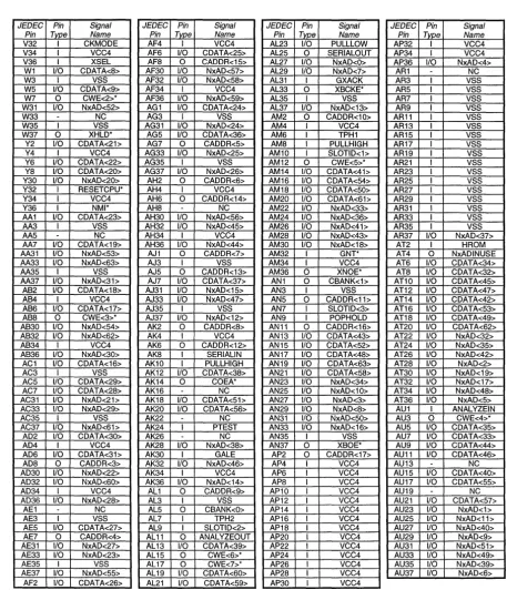
Nx586 Pinouts by Signal Names
PGA JEDEC Pin Signal PGA JEDEC Pin Signal PGA JEDEC Pin Signal
Pin# Pin# Type Name Pin# Pin# Tvpe Name Pin# Pin# Tvpe Name
449 J37 0 ALE* 195 AT14 I/O CDATA<42> 12 AE1 - NC 18 AU1 I ANALYZEIN 185 AN13 I/O CDATA<43> 17 AR1
-
NC 168 AL11 0 ANALYZEOUT 155 AU9 I/O CDATA<44> 19 B2-
NC 340 N31 0 AREQ* 163 AT10 I/O CDATA<45> 20 D2-
NC 34 AM2 0 CADDR<10> 171 AU11 I/O CDATA<46> 21 F2 - NC 90 AN5 0 CADDR<11> 179 AT12 I/O CDATA<47> 22 H2-
NC 107 AK6 0 CADDR<12> 217 AN17 I/O CDATA<48> 23 K2-
NC 88 AJ5 0 CADDR<13> 227 AT18 I/O CDATA<49> 25 P2-
NC 106 AH6 0 CADDR<14> 80 N5 I/O CDATA<5> 37 A3-
NC 142 AF8 0 CADDR<15> 225 AM18 I/O CDATA<50> 56 B4-
NC 169 AN11 0 CADDR<16> 224 AK18 I/O CDATA<51 > 74 A5 NC 35 AP2 0 CADDR<17> 201 AN15 I/O CDATA<52> 77 G5-
NC 141 AD8 0 CADDR<3> 211 AT16 I/O CDATA<53> 78 J5 NC 123 AE7 0 CADDR<4> 209 AM16 I/O CDATA<54> 79 L5-
NC 124 AF7 0 CADDR<5> 219 AU17 I/O CDATA<55> 84 AA5 NC 32 AH2 0 CADDR<6> 240 AK20 I/O CDATA<56> 93 B6-
NC 14 AJ1 0 CADDR<7> 251 AU21 I/O CDATA<57> 95 F6-
NC 33 AK2 0 CADDR<8> 249 AN21 I/O CDATA<58> 96 H6 NC 15 AL1 0 CADDR<9> 248 AL21 I/O CDATA<59> 97 K6-
NC 89 AL5 0 CBANK<O> 6 N1 I/O CDATA<6> 98 M6 NC 16 AN1 0 CBANK<1> 232 AL19 I/O CDATA<60> 101 V6 NC 100 T6 I/O CDATA<O> 241 AM20 I/O CDATA<61> 111 A7 NC 7 R1 I/O CDATA<1> 243 AT20 I/O CDATA<62> 114 G7 NC 27 V2 I/O CDATA<10> 233 AN19 I/O CDATA<63> 115 J7 NC 119 U7 I/O CDATA<11> 99 P6 I/O CDATA<7> 116 L7 NC 118 R7 I/O CDATA<12> 9 W1 I/O CDATA<8> 132 F8 NC 26 T2 I/O CDATA<13> 83 W5 I/O CDATA<9> 133 H8 NC 82 U5 I/O CDATA<14> 361 V32 I CKMODE 134 K8 NC 8 U1 I/O CDATA<15> 192 AK14 0 COEA* 135 M8 NC 11 AC1 I/O CDATA<16> 138 V8 0 COEB* 143 AH8 NC 103 AB6 I/O CDATA<17> 117 N7 0 CWE<O>* 148 A9 NC 29 K2 I/O CDATA<18> 137 T8 0 CWE<1>* 151 G9-
NC 121 AA7 I/O CDATA<19> 120 W7 0 CWE<2>* 156 B10 NC 81 R5 I/O CDATA<2> 140 AB8 0 CWE<3>* 158 F10-
NC 139 Y8 I/O CDATA<20> 55 AU3 0 CWE<4>* 159 H10 NC 28 Y2 I/O CDATA<21> 177 AM12 0 CWE<5>* 164 A11 - NC 102 Y6 I/O CDATA<22> 200 AL15 0 CWE<6>* 166 E11 NC 10 AA1 I/O CDATA<23> 216 AL17 0 CWE<7>* 167 G11-
NC 13 AG1 I/O CDATA<24> 359 P32 0 DCL* 172 B12 NC 105 AF6 I/O CDATA<25> 330 AK30 GALE 174 F12 - NC 31 AF2 I/O CDATA<26> 339 L31 GATEA20 175 H12 NC 86 AE5 I/O CDATA<27> 378 R33 GBLKNBL 180 A13-
NC 122 AC7 I/O CDATA<28> 429 F36 GDCL 182 E13 - NC 85 AC5 I/O CDATA<29> 368 AM32 GNT* 183 G13-
NC 136 P8 I/O CDATA<3> 113 E7 GREF 187 AU13-
NC 30 AD2 I/O CDATA<30> 430 H36 GSHARE 188 B14-
NC 104 AD6 I/O CDATA<31> 322 P30 GTAL 190 F14-
NC 147 AT8 I/O CDATA<32> 349 AL31 GXACK 191 H14-
NC 129 AU7 I/O CDATA<33> 3n N33 GXHLD 196 A15 NC110 AT6 I/O CDATA<34> 36 AT2 HROM 198 E15 NC
92 AU5 I/O CDATA<35> 375 J33 INTR* 199 G15
-
NC87 AG5 I/O CDATA<36> 323 T30 IREF 204 B16 NC
125 AJ7 I/O CDATA<37> 341 R31 0 LOCK* 206 F16
-
NC176 AK12 I/O CDATA<38> 1 C1 NC 207 H16 NC
184 AL13 I/O CDATA<39> 2 E1
-
NC 208 AK16-
NC24 M2 I/O CDATA<4> 3 G1 NC 212 A17 NC
203 AU15 I/O CDATA<40> 4 J1 NC 215 G17 NC
193 AM14 I/O CDATA<41> 5 L1 NC 220 B18 NC
Figure 3 Nx586 Pin List, By Signal Name
NexGen™
Nx586 Features and SignalsPGA JEDEC Pin Signal PGA JEDEC Pin Signal PGA JEDEC Pin Signal Pin# Pin# Tvpe Name Pin# Pin# Tvpe Name Pin# Pin# TJ'Qe Name
222 F18 NC 267 AU23 liD NxAD<1> 439 AF36 liD NxAD<59> 223 H18 NC 307 AT28 liD NxAD<2> 364 AD32 lID NxAD<60> 228 A19 NC 297 AN27 liD NxAD<3> 456 AC37 lID NxAD<61> 230 E19 NC 443 AP36 liD NxAD<4> 363 A832 lID NxAD<62> 231 G19 NC 444 AT36 liD NxAD<5> 381 AA33 I/O NxAD<63> 235 AU19
-
NC 463 AU37 lID NxAD<6> 73 AT4 0 NxADINUSE236 820 NC 312 AL29 lID NxAD<7> 452 R37 NxCLK
238 F20 NC 313 AN29 I/O NxAD<8> 447 E37 OWNA8L
239 H2O NC 315 AU29 lID NxAD<9> 76 E5 P4REF
244 A21 NC 281 AN25 lID NxAD<10> 453 U37 PHE1
246 E21 - NC 283 AU25 lID NxAD<11> 379 U33 PHE2 247 G21 - NC 459 AJ37 lID NxAD<12> 153 AN9 POPHOLD 252 822
-
NC 460 AL37 liD NxAD<13> 272 AK24 PTEST 254 F22 NC 441 AK36 lID NxAD<14> 319 H30 PULLDOWN 255 H22 NC 348 AJ31 lID NxAD<15> 355 F32 PULLDOWN 256 AK22-
NC 387 AN33 lID NxAD<16> 160 AK10 PULLHIGH 260 A23 - NC 370 AT32 lID NxAD<17> 145 AM8 PULLHIGH 262 E23-
NC 331 AM30 liD NxAD<18> 357 K32 0 PULLHIGH 263 G23 - NC 333 AT30 lID NxAD<19> 376 L33 lID PULLHIGH 268 824 NC 325 Y30 I/O NxAD<20> 432 M36 lID PULLHIGH 270 F24 - NC 345 AC31 I/O NxAD<21> 433 P36 lID PULLHIGH 271 H24-
NC 327 AD30 liD NxAD<22> 450 L37 lID PULLHIGH 276 A25 NC 383 AE33 lID NxAD<23> 451 N37 lID PULLHIGH 278 E25 - NC 347 AG31 lID NxAD<24> 264 AL23 lID PULLLOW 279 G25 NC 384 AG33 lID NxAD<25> 214 E17 I RESET* 284 826 - NC 458 AG37 lID NxAD<26> 362 Y32 I RESETCPU* 286 F26 - NC 346 AE31 I/O NxAD<27> 150 E9 lID SCLKE 287 H26 - NC 438 AD36 lID NxAD<28> 144 AK8 I SERIALIN 288 AK26 - NC 382 AC33 lID NxAD<29> 280 AL25 0 SERIALOUT 292 A27 NC 437 A836 lID NxAD<30> 448 G37 0 SHARE* 294 E27 NC 455 AA37 lID NxAD<31> 130 88 I SLOTID<O> 295 G27 - NC 259 AT22 lID NxAD<32> 161 AM10 I SLOTID<1> 300 828-
NC 257 AM22 lID NxAD<33> 152 AL9 I SLOTID<2> 302 F28-
NC 265 AN23 lID NxAD<34> 127 AN7 I SLOTID<3> 303 H28 NC 275 AT24 lID NxAD<35> 431 K36 liD SRAMMODE 308 A29 - NC 273 AM24 lID NxAD<36> 374 G33 TESTPWR* 310 E29-
NC 462 AR37 lID NxAD<37> 108 AM6 TPH1 311 G29 - NC 304 AK28 lID NxAD<38> 126 AL7 TPH2316 830 NC 426 AU35 lID NxAD<39> 57 E4 VCC4
318 F30 - NC 299 AU27 lID NxAD<40> 58 F4 VCC4
334 A31
-
NC 289 AM26 lID NxAD<41> 59 H4 VCC4336 E31 NC 291 AT26 I/O NxAD<42> 60 K4 VCC4
337 G31 NC 305 AM28 lID NxAD<43> 61 M4 VCC4
338 J31 NC 440 AH36 lID NxAD<44> 62 P4 VCC4
353 832 NC 366 AH32 lID NxAD<45> 63 T4 VCC4
356 H32 NC 367 AK32 lID NxAD<46> 64 V4 VCC4
371 A33 - NC 385 AJ33 liD NxAD<47> 65 Y4 VCC4
373 E33 - NC 407 AT34 lID NxAD<48> 66 A84 VCC4
380 W33 - NC 389 AU33 lID NxAD<49> 67 AD4 VCC4
390 834 NC 350 AN31 lID NxAD<50> 68 AF4 VCC4
408 A35 NC 352 AU31 lID NxAD<51> 69 AH4 VCC4
427 836 NC 343 W31 lID NxAD<52> 70 AK4 VCC4
428 036 NC 344 AA31 lID NxAD<53> 71 AM4 VCC4
445 A37 NC 326 A830 lID NxAD<54> 72 AP4 VCC4
[image:18.615.104.533.124.633.2]436 Y36 I NMI* 457 AE37 lID NxAD<55> 94 06 VCC4 446 C37 0 NPIRO* 329 AH30 liD NxAD<56> 109 AP6 VCC4 321 M30 0 NREO* 328 AF30 lID NxAD<57> 131 08 VCC4 296 AL27 liD NxAD<O> 365 AF32 liD NxAD<58> 146 AP8 VCC4
Figure 3 Nx586 Pin List, By Signal Name (continued)
Nx586 Features and Signals
NexGen
lMPGA JEDEC Pin Signal PGA JEDEC Pin Signal PGA JEDEC Pin Signal
Pin# Pin# Type Name Pin# Pin# Type Name Pin# Pin# Type Name
157 010 VCC4 324 V30 VOOA 261 C23 VSS
162 AP10 VCC4 38 C3 VSS 266 AR23 VSS
173 012 VCC4 39 E3 VSS 277 C25 VSS
178 AP12 VCC4 40 G3 VSS 282 AR25 VSS
189 014 VCC4 41 J3 VSS 293 C27 VSS
194 AP14 VCC4 42 L3 VSS 298 AR27 VSS
205 016 VCC4 43 N3 VSS 309 C29 VSS
210 AP16 VCC4 44 R3 VSS 314 AR29 VSS
221 018 VCC4 45 U3 VSS 335 C31 VSS
226 AP18 VCC4 46 W3 VSS 351 AR31 VSS
237 020 VCC4 47 AA3 VSS 372 C33 VSS
242 AP20 VCC4 48 AC3 VSS 388 AR33 VSS
253 022 VCC4 49 AE3 VSS 409 C35 VSS
258 AP22 VCC4 50 AG3 VSS 410 E35 VSS
269 024 VCC4 51 AJ3 VSS 411 G35 VSS
274 AP24 VCC4 52 AL3 VSS 412 J35 VSS
285 026 VCC4 53 AN3 VSS 413 L35 VSS
290 AP26 VCC4 54 AR3 VSS 414 N35 VSS
301 028 VCC4 75 C5 VSS 415 R35 VSS
306 AP28 VCC4 91 AR5 VSS 416 U35 VSS
317 030 VCC4 112 C7 VSS 417 W35 VSS
332 AP30 VCC4 128 AR7 VSS 418 AA35 VSS
354 032 VCC4 149 C9 VSS 419 AC35 VSS
369 AP32 VCC4 154 AR9 VSS 420 AE35 VSS
391 034 VCC4 165 C11 VSS 421 AG35 VSS
392 F34 VCC4 170 AR11 VSS 422 AJ35 VSS
393 H34 VCC4 181 C13 VSS 423 AL35 VSS
394 K34 VCC4 186 AR13 VSS 424 AN35 VSS
395 M34 VCC4 197 C15 VSS 425 AR35 VSS
396 P34 VCC4 202 AR15 VSS 358 M32 0 XACK*
397 T34 VCC4 213 C17 VSS 386 AL33 0 XBCKE*
398 V34 VCC4 218 AR17 VSS 461 AN37 0 XBOE*
399 Y34 VCC4 229 C19 VSS 320 K30 1/0 XCVERE*
400 AB34 VCC4 234 AR19 VSS 454 W37 0 XHLO*
401 A034 VCC4 245 C21 VSS 442 AM36 0 XNOE*
402 AF34 VCC4 250 AR21 VSS 360 T32 0 XPH1
403 AH34 VCC4 54 AR3 VSS 342 U31 0 XPH2
404 AK34 VCC4 75 C5 VSS 434 T36 0 XREF
405 AM34 VCC4 91 AR5 VSS 435 V36 I XSEL
[image:19.617.83.498.131.731.2]406 AP34 VCC4 112 C7 VSS
Figure 3 Nx586 Pin List, By Signal Name (continued)
8 Nx586lM
NexGen
lMNx586 Features and Signals
Nx586 Pinouts by PGA Pin Numbers
PGA Pin Signal PGA Pin Signal PGA Pin Signal PGA Pin Signal
Pin Tvpe Name Pin Tvpe Name Pin Tvpe Name Pin Tvpe Name
1 NC 57 VCC4 113 I GREF 169 0 CADDR<16>
2 NC 58 VCC4 114 I PULLHIGH 170 I VSS
3 NC 59 VCC4 115 NC 171 I/O CDATA<46>
4 NC 60 VCC4 116
-
NC 172 NC5 I/O NPTAG<O> 61 VCC4 117 0 CWE<O>* 173 I VCC4 6 I/O CDATA<6> 62 VCC4 118 I/O CDATA<12> 174
-
NC 7 I/O CDATA<1> 63 VCC4 119 I/O CDATA<11> 175 - NC 8 I/O CDATA<15> 64 VCC4 120 0 CWE<2>* 176 I/O CDATA<38> 9 I/O CDATA<8> 65 VCC4 121 I/O CDATA<19> 177 0 CWE<5>* 10 I/O CDATA<23> 66 VCC4 122 I/O CDATA<28> 178 I VCC4 11 I/O CDATA<16> 67 VCC4 123 0 CADDR<4> 179 I/O CDATA<47>12 NC 68 VCC4 124 0 CADDR<5> 180 NC
13 I/O CDATA<24> 69 VCC4 125 I/O CDATA<37> 181 I VSS
14 0 CADDR<7> 70 VCC4 126 I TPH2 182 - NC
15 0 CADDR<9> 71 VCC4 127 I SLOTID<3> 183
-
NC 16 0 CBANK<1> 72 VCC4 128 I VSS 184 I/O CDATA<39> 17 NC 73 0 NxADINUSE 129 I/O CDATA<33> 185 I/O CDATA<43> 18 I ANALYZEIN 74 NC 130 I SLOTID<O> 186 I VSS19 - NC 75 I VSS 131 I VCC4 187
-
NC20 NC 76 I P4REF 132 NC 188 NC
21 NC 77 NC 133 I PULLHIGH 189 I VCC4
22 NC 78 NC 134 NC 190
-
NC23 NC 79 NC 135 NC 191 - NC
24 I/O CDATA<4> 80 I/O CDATA<5> 136 I/O CDATA<3> 192 0 COEA* 25 NC 81 I/O CDATA<2> 137 0 CWE<1>* 193 I/O CDATA<41> 26 I/O CDATA<13> 82 I/O CDATA<14> 138 0 COEB* 194 I VCC4 27 I/O CDATA<10> 83 I/O CDATA<9> 139 I/O CDATA<20> 195 I/O CDATA<42> 28 I/O CDATA<21> 84 NC 140 0 CWE<3>* 196 - NC 29 110 CDATA<18> 85 I/O CDATA<29> 141 0 CADDR<3> 197 I VSS 30 I/O CDATA<30> 86 110 CDATA<27> 142 0 CADDR<15> 198 - NC 31 I/O CDATA<26> 87 I/O CDATA<36> 143 NC 199
-
NC 32 0 CADDR<6> 88 0 CADDR<13> 144 I SERIALIN 200 0 CWE<6>* 33 0 CADDR<8> 89 0 CBANK<O> 145 I PULLHIGH 201 I/O CDATA<52> 34 0 CADDR<10> 90 0 CADDR<11> 146 I VCC4 202 I VSS 35 0 CADDR<17> 91 I VSS 147 I/O CDATA<32> 203 I/O CDATA<40>36 HROM 92 I/O CDATA<35> 148 NC 204 NC
37 NC 93 NC 149 I VSS 205 I VCC4
38 VSS 94 I VCC4 150 110 SCLKE 206
-
NC39 VSS 95 NC 151 NC 207 - NC
40 VSS 96 NC 152 I SLOTID<2> 208
-
NC41 VSS 97 NC 153 I POPHOLD 209 I/O CDATA<54>
42 VSS 98 NC 154 I VSS 210 I VCC4
43 VSS 99 I/O CDATA<7> 155 I/O CDATA<44> 211 I/O CDATA<53>
44 VSS 100 I/O CDATA<O> 156 - NC 212 - NC
45 VSS 101 NC 157 I VCC4 213 I VSS
46 VSS 102 I/O CDATA<22> 158 NC 214 I RESEr
47 VSS 103 I/O CDATA<17> 159 NC 215 - NC
48 VSS 104 I/O CDATA<31 > 160 I PULLHIGH 216 0 CWE<7>* 49 VSS 105 I/O CDATA<25> 161 I SLOTID<1> 217 I/O CDATA<48>
50 VSS 106 0 CADDR<14> 162 I VCC4 218 I VSS
51 VSS 107 0 CADDR<12> 163 I/O CDATA<45> 219 I/O CDATA<55>
52 VSS 108 I TPH1 164 NC 220
-
NC53 VSS 109 I VCC4 165 I VSS 221 I VCC4
54 VSS 110 I/O CDATA<34> 166 NC 222 NC
[image:20.615.108.541.129.660.2]55 0 CWE<4>* 111 I/O NPTAG<3> 167 NC 223 NC 56 NC 112 I VSS 168 0 ANALYZEOUT 224 I/O CDATA<51>
Figure 4 Nx586 Pin List, By PGA Pin Number
PRELIMINARY Nx586lM
Nx586 Features and Signals
NexGen™
PGA Pin Signal PGA Pin Signal PGA Pin Signal PGA Pin Signal
Pin Type Name Pin Type Name Pin Type Name Pin Type Name
225 I/O CDATA<50> 285 I VCC4 345 I/O NxAD<21> 405 I VCC4
226 I VCC4 286 NC 346 I/O NxAD<27> 406 I VCC4
227 I/O CDATA<49> 287 NC 347 I/O NxAD<24> 407 I/O NxAD<48>
228 NC 288 - NC 348 I/O NxAD<15> 408 NC
229 I VSS 289 I/O NxAD<41> 349 I GXACK 409 VSS
230 NC 290 I VCC4 350 I/O NxAD<50> 410 VSS
231 NC 291 I/O NxAD<42> 351 I VSS 411 VSS
232 I/O CDATA<60> 292
-
NC 352 I/O NxAD<51> 412 VSS233 I/O CDATA<63> 293 I VSS 353 NC 413 VSS
234 I VSS 294 NC 354 I VCC4 414 VSS
235 NC 295 NC 355 I PULLDOWN 415 VSS
236 NC 296 I/O NxAD<O> 356 NC 416 VSS
237 I VCC4 297 I/O NxAD<3> 357 I/O PULLHIGH 417 VSS
238 NC 298 I VSS 358 0 XACK* 418 VSS
239 NC 299 I/O NxAD<40> 359 0 DCL* 419 VSS
240 I/O CDATA<56> 300 NC 360 0 XPH1 420 VSS
241 I/O CDATA<61> 301 I VCC4 361 I CKMODE 421 VSS
242 I VCC4 302 - NC 362 I RESETCPU* 422 VSS
243 I/O CDATA<62> 303 NC 363 I/O NxAD<62> 423 VSS 244
-
NC 304 I/O NxAD<38> 364 I/O NxAD<60> 424 VSS 245 I VSS 305 I/O NxAD<43> 365 I/O NxAD<58> 425 VSS 246 NC 306 I VCC4 366 I/O NxAD<45> 426 10 NxAD<39> 247 NC 307 I/O NxAD<2> 367 I/O NxAD<46> 427--
NC 248 I/O CDATA<59> 308-
NC 368 I GNT* 428 -- NC 249 I/O CDATA<58> 309 I VSS 369 I VCC4 429 I GDCL250 I VSS 310 NC 370 I/O NxAD<17> 430 I GSHARE
251 I/O CDATA<57> 311 NC 371 I/O NPDATA<54> 431 I/O SRAMMODE 252 NC 312 I/O NxAD<7> 372 I VSS 432 I/O PULLHIGH 253 I VCC4 313 I/O NxAD<8> 373 I/O NPDATA<42> 433 I/O PULLHIGH
254 NC 314 I VSS 374 I TESTPWR* 434 0 XREF
255 - NC 315 I/O NxAD<9> 375 I INTR* 435 I XSEL
256 NC 316 NC 376 I/O PULLHIGH 436 I NMI*
257 I/O NxAD<33> 317 I VCC4 377 I GXHLD 437 I/O NxAD<30> 258 I VCC4 318 NC 378 I GBLKNBL 438 I/O NxAD<28> 259 I/O NxAD<32> 319 I PULLDOWN 379 I PHE2 439 I/O NxAD<59> 260
-
NC 320 I XCVERE* 380-
NC 440 I/O NxAD<44> 261 I VSS 321 0 NREQ* 381 I/O NxAD<63> 441 I/O NxAD<14> 262 NC 322 I GTAL 382 I/O NxAD<29> 442 0 XNOE* 263 - NC 323 I IREF 383 I/O NxAD<23> 443 I/O NxAD<4> 264 I/O PULLLOW 324 I VDDA 384 I/O NxAD<25> 444 I/O NxAD<5> 265 I/O NxAD<34> 325 I/O NxAD<20> 385 I/O NxAD<47> 445 NC 266 I VSS 326 I/O NxAD<54> 386 0 XBCKE* 446 0 NPIRQ* 267 I/O NxAD<1> 327 I/O NxAD<22> 387 I/O NxAD<16> 447 I OWNABL 268 NC 328 I/O NxAD<57> 388 I VSS 448 0 SHARE* 269 I VCC4 329 I/O NxAD<56> 389 I/O NxAD<49> 449 0 ALE*270 NC 330 I GALE 390 NC 450 I/O PULLHIGH
271 - NC 331 I/O NxAD<18> 391 VCC4 451 I/O PULLHIGH
272 I PTEST 332 I VCC4 392 VCC4 452 I NxCLK
273 I/O NxAD<36> 333 I/O NxAD<19> 393 VCC4 453 I PHE1
274 I VCC4 334 NC 394 VCC4 454 0 XHLD*
275 I/O NxAD<35> 335 I VSS 395 VCC4 455 I/O NxAD<31>
276 - NC 336 - NC 396 VCC4 456 I/O NxAD<61>
277 I VSS 337 I PULLHIGH 397 VCC4 457 I/O NxAD<55>
278
-
NC 338 NC 398 VCC4 458 I/O NxAD<26>279 NC 339 I GATEA20 399 VCC4 459 I/O NxAD<12>
280 0 SERIALOUT 340 0 AREQ* 400 VCC4 460 I/O NxAD<13> 281 I/O NxAD<10> 341 0 LOCK* 401 VCC4 461 0 XBOE*
282 I VSS 342 0 XPH2 402 VCC4 462 I/O NxAD<37>
283 I/O NxAD<11> 343 I/O NxAD<52> 403 VCC4 463 I/O NxAD<6>
[image:21.617.75.513.122.659.2]284 NC 344 I/O NxAD<53> 404 VCC4
Figure 4 Nx586 Pin List, By PGA Pin Number (continued)
NexGen
lMNx586 Features and Signals
Nx586 Pinouts by JEDEC Pin Numbers
JEDEC Pin Signal JEDEC Pin Signal JEDEC Pin Signal JEDEC Pin Signal
Pin Tvpe Name Pin Type Name Pin Type Name Pin Tvpe Name
A3
-
NC 04 VCC4 G5 NC L33 I/O PULLHIGHA5 - NC 06 VCC4 G7 I PULLHIGH L35 I VSS
A7 I/O NPTAG<3> 08 VCC4 G9
-
NC L37 I/O PULLHIGHA9 NC 010 VCC4 G11 NC M2 I/O COATA<4>
A11 - NC 012 VCC4 G13 NC M4 I VCC4
A13 - NC 014 VCC4 G15 NC M6
-
NCA15 - NC 016 VCC4 G17 NC M8 - NC
A17
-
NC 018 VCC4 G19 NC M30 0 NREO'A19 NC 020 VCC4 G21 - NC M32 0 XACK'
A21
-
NC 022 VCC4 G23 NC M34 I VCC4A23 NC 024 VCC4 G25 NC M36 I/O PULLHIGH
A25
-
NC 026 VCC4 G27 NC N1 I/O COATA<6>A27 NC 028 VCC4 G29 NC N3 I VSS
A29
-
NC 030 VCC4 G31 I PULLHIGH N5 I/O COATA<5>A31 NC 032 VCC4 G33 I TESTPWR' N7 0 CWE<O>'
A33 I/O NPOATA<54> 034 VCC4 G35 I VSS N31 0 AREO'
A35 NC 036 NC G37 0 SHARE' N33 I GXHLO
A37 NC E1 NC H2 NC N35 I VSS
82 - NC E3 VSS H4 I VCC4 N37 I/O PULLHIGH
84 NC E5 P4REF H6 NC P2 - NC
86 NC E7 GREF H8 I PULLHIGH P4 I VCC4
88 I SLOTIO<O> E9 I/O SCLKE H10 NC P6 I/O COATA<7>
810 NC E11 NC H12 NC P8 I/O COATA<3>
812 - NC E13 NC H14 NC P30 I GTAL
814 NC E15 NC H16
-
NC P32 0 OCL'816 NC E17 I RESET' H18 NC P34 I VCC4
818
-
NC E19 NC H2O NC P36 I/O PULLHIGH820 NC E21 NC H22 NC R1 I/O COATA<1>
822 NC E23 NC H24 NC R3 I VSS
824 NC E25 NC H26 NC R5 I/O COATA<2>
826 NC E27 NC H28 NC R7 I/O COATA<12>
828 NC E29 NC H30 I PULLOOWN R31 0 LOCK'
830 - NC E31 NC H32 NC R33 I G8LKNBL
832 NC E33 I/O NPOATA<42> . H34 I VCC4 R35 I VSS
834 - NC E35 I VSS H36 I GSHARE R37 I NxCLK
836 -- NC E37 I OWNA8L J1 NC T2 I/O COATA<13>
C1 NC F2
-
NC J3 I VSS T4 I VCC4C3 I VSS F4 I VCC4 J5 NC T6 I/O COATA<O>
C5 I VSS F6
-
NC J7 NC T8 0 CWE<1>'C7 I VSS F8 - NC J31 NC T30 I IREF
C9 I VSS F10
-
NC J33 I INTR' T32 0 XPH1C11 I VSS F12 - NC J35 I VSS T34 I VCC4
C13 I VSS F14 NC J37 0 ALE' T36 0 XREF
C15 I VSS F16
-
NC K2 NC U1 I/O COATA<15>C17 I VSS F18 NC K4 I VCC4 U3 I VSS
C19 I VSS F20
-
NC K6 NC U5 I/O COATA<14>C21 I VSS F22
-
NC K8-
NC U7 I/O COATA<11>C23 I VSS F24 - NC K30 I/O XCVERE' U31 0 XPH2
C25 I VSS F26 NC K32 I/O PULLHIGH U33 I PHE2
C27 I VSS F28
-
NC K34 I VCC4 U35 I VSSC29 I VSS F30 NC K36 I/O SRAMMOOE U37 I PHE1
C31 I VSS F32 I PULLOOWN L1 I/O NPTAG<O> V2 I/O COATA<10>
C33 I VSS F34 I VCC4 L3 I VSS V4 I VCC4
C35 I VSS F36 I GOCL L5
-
NC V6 NCC37 0 NPIRO' G1 NC L7 NC V8 0 COE8'
[image:22.621.95.538.124.639.2]02 NC G3 I VSS L31 I GATEA20 V30 I VOOA
Figure 5 Nx586 Pin List, By JEDEC Pin Number
Nx586 Features and Signals
NexGen
lMJEDEC Pin Signal JEDEC Pin Signal JEDEC Pin Signal JEDEC Pin Signal Pin Type Name Pin Tvpe Name Pin Type Name Pin Type Name
V32 I CKMODE AF4 I VCC4 AL23 I/O PULLLOW AP32 I VCC4
V34 I VCC4 AF6 I/O CDATA<25> AL25 0 SERIALOUT AP34 I VCC4 V36 I XSEL AF8 0 CADDR<15> AL27 I/O NxAD<O> AP36 I/O NxAD<4>
W1 I/O CDATA<8> AF30 I/O NxAD<57> AL29 I/O NxAD<7> AR1 NC W3 I VSS AF32 I/O NxAD<58> AL31 I GXACK AR3 VSS W5 I/O CDATA<9> AF34 I VCC4 AL33 0 XBCKE* AR5 VSS W7 0 CWE<2>* AF36 I/O NxAD<59> AL35 I VSS AR7 VSS W31 I/O NxAD<52> AG1 I/O CDATA<24> AL37 I/O NxAD<13> AR9 VSS
W33
-
NC AG3 I VSS AM2 0 CADDR<10> AR11 VSSW35 I VSS AG31 I/O NxAD<24> AM4 I VCC4 AR13 VSS W37 0 XHLD* AG5 I/O CDATA<36> AM6 I TPH1 AR15 VSS Y2 I/O CDATA<21> AG7 0 CADDR<5> AM8 I PULLHIGH AR17 VSS Y4 I VCC4 AG33 I/O NxAD<25> AM10 I SLOTID<1> AR19 VSS Y6 I/O CDATA<22> AG35 I VSS AM12 0 CWE<5>* AR21 VSS Y8 I/O CDATA<20> AG37 I/O NxAD<26> AM14 I/O CDATA<41> AR23 VSS Y30 I/O NxAD<20> AH2 0 CADDR<6> AM16 I/O CDATA<54> AR25 VSS Y32 I RESETCPU* AH4 I VCC4 AM18 I/O CDATA<50> AR27 VSS Y34 I VCC4 AH6 0 CADDR<14> AM20 I/O CDATA<61> AR29 VSS
Y36 I NMI* AH8 NC AM22 I/O NxAD<33> AR31 VSS
AA1 I/O CDATA<23> AH30 I/O NxAD<56> AM24 I/O NxAD<36> AR33 VSS AA3 I VSS AH32 I/O NxAD<45> AM26 I/O NxAD<41> AR35 VSS AA5
-
NC AH34 I VCC4 AM28 I/O NxAD<43> AR37 I/O NxAD<37> AA7 I/O CDATA<19> AH36 I/O NxAD<44> AM30 I/O NxAD<18> AT2 I HROM AA31 I/O NxAD<53> AJ1 0 CADDR<7> AM32 I GNP AT4 0 NxADINUSE AA33 I/O NxAD<63> AJ3 I VSS AM34 I VCC4 AT6 I/O CDATA<34> AA35 I VSS AJ5 0 CADDR<13> AM36 0 XNOE* AT8 I/O CDATA<32> AA37 I/O NxAD<31> AJ7 I/O CDATA<37> AN1 0 CBANK<1> AT10 I/O CDATA<45> AB2 I/O CDATA<18> AJ31 I/O NxAD<15> AN3 I VSS AT12 I/O CDATA<47> AB4 I VCC4 AJ33 I/O NxAD<47> AN5 0 CADDR<11> AT14 I/O CDATA<42> AB6 I/O CDATA<17> AJ35 I VSS AN7 I SLOTID<3> AT16 I/O CDATA<53> AB8 0 CWE<3>* AJ37 I/O NxAD<12> AN9 I POPHOLD AT18 I/O CDATA<49> AB30 I/O NxAD<54> AK2 0 CADDR<8> AN11 0 CADDR<16> AT20 I/O CDATA<62> AB32 I/O NxAD<62> AK4 I VCC4 AN13 I/O CDATA<43> AT22 I/O NxAD<32> AB34 I VCC4 AK6 0 CADDR<12> AN15 I/O CDATA<52> AT24 I/O NxAD<35> AB36 I/O NxAD<30> AK8 I SERIALIN AN17 I/O CDATA<48> AT26 I/O NxAD<42> AC1 I/O CDATA<16> AK10 I PULLHIGH AN19 I/O CDATA<63> AT28 I/O NxAD<2> AC3 I VSS AK12 I/O CDATA<38> AN21 I/O CDATA<58> AT30 I/O NxAD<19> AC5 I/O CDATA<29> AK14 0 COEA* AN23 I/O NxAD<34> AT32 liD NxAD<17> AC7 I/O CDATA<28> AK16-
NC AN25 I/O NxAD<10> AT34 I/O NxAD<48> AC31 I/O NxAD<21> AK18 I/O CDATA<51> AN27 I/O NxAD<3> AT36 I/O NxAD<5> AC33 I/O NxAD<29> AK20 I/O CDATA<56> AN29 I/O NxAD<8> AU1 I ANALYZEIN AC35 I VSS AK22 NC AN31 I/O NxAD<50> AU3 0 CWE<4>* AC37 I/O NxAD<61> AK24 I PTEST AN33 I/O NxAD<16> AU5 I/O CDATA<35>AD2 I/O CDATA<30> AK26
-
NC AN35 I VSS AU7 I/O CDATA<33> AD4 I VCC4 AK28 I/O NxAD<38> AN37 0 XBOE* AU9 I/O CDATA<44> AD6 I/O CDATA<31> AK30 I GALE AP2 0 CADDR<17> AU11 I/O CDATA<46> AD8 0 CADDR<3> AK32 I/O NxAD<46> AP4 I VCC4 AU13 NC AD30 I/O NxAD<22> AK34 I VCC4 AP6 I VCC4 AU15 I/O CDATA<40> AD32 I/O NxAD<60> AK36 I/O NxAD<14> AP8 I VCC4 AU 17 I/O CDATA<55>AD34 I VCC4 AL1 0 CADDR<9> AP10 I VCC4 AU19 NC
AD36 I/O NxAD<28> AL3 I VSS AP12 I VCC4 AU21 I/O CDATA<57> AE1 NC AL5 0 CBANK<O> AP14 I VCC4 AU23 I/O NxAD<1> AE3 I VSS AL7 I TPH2 AP16 I VCC4 AU25 I/O NxAD<11> AE5 I/O CDATA<27> AL9 I SLOTID<2> AP18 I VCC4 AU27 I/O NxAD<40> AE7 0 CADDR<4> AL11 0 ANALYZEOUT AP20 I VCC4 AU29 I/O NxAD<9> AE31 I/O NxAD<27> AL13 I/O CDATA<39> AP22 I VCC4 AU31 I/O NxAD<51> AE33 I/O NxAD<23> AL15 0 CWE<6>* AP24 I VCC4 AU33 I/O NxAD<49> AE35 I VSS AL17 0 CWE<7>* AP26 I VCC4 AU35 I/O NxAD<39> AE37 I/O NxAD<55> AL19 I/O CDATA<60> AP28 I VCC4 AU37 I/O NxAD<6>
[image:23.618.70.528.115.647.2]AF2 I/O CDATA<26> AL21 I/O CDATA<59> AP30 I VCC4
Figure 5 Nx586 Pin List, By JEDEC Pin Number (continued)
12 Nx586lM
NexGen
lMNx586 Features and Signals
Figure 6 Nx586 PGA Pinout Diagram (Top View)
PRELIMINARY Nx586lM
Nx586 Features and Signals
NexGen
lMFigure 7 Nx586 PGA Pinout Diagram (Bottom View)
14 Nx586lM
NexGen
lM Nx586 Features and Signals36 34 32 30 28 26 24 22 20 18 16 14 12 10 8 6 4 2
37 35 33 31 29 27 25 23 21 19 17 15 13 11 9 7 5 3 1
Figure 8 Nx586 JEDEC Pinout Diagram (Top View)
PRELIMINARY Nx586lM
Nx586 Features and Signals
NexGen™
2 4 6 8 1 0 12 14 16 18 20 22 24 26 28 30 32 34 36
1 3 5 7 9 11 13 15 17 19 21 23 25 27 29 31 33 35 37
Figure 9 Nx586 JEDEC Pinout Diagram (Bottom View)
NexGen
lMNx586 Features and Signals
Nx586 NexBus/NexBus5 Signals
NexBus/NexBus5 Arbitration
NREQ*
o
AREQ*
o
GNT* I
PRELIMINARY
NexBus Request-Asserted by the processor to the NexBus5 arbiter to secure control of the system bus. The Nx586 will drive NREQ* active on the rising edge of NxCLK. The bus is granted when the arbiter asserts GNT*. The "grant" becomes effective only when the Nx586 asserts ALE* or LOCK*. This signal remains active until one NxCLK period after GALE is received from the NexBus arbiter. During speculative reads, the Nx586 may deactivate NREQ* before GNT* is received if the transfer is no longer needed.
If the processor does not know which bus its intended resource is on, it asserts NREQ*. If a GTAL is subsequently returned, the processor assumes the resources are on another system bus and it retries the transfer by asserting AREQ* . The processor at anytime may perform speculative cycles that prematurely terminate. This is done by asserting NREQ* and then subsequently removing NREQ* before GNT* is asserted.
Alternate-Bus Request-Asserted by the processor to the NexBus arbiter to secure control of the system bus and any other buses (called alternate buses) supported by the system. This signal remains active until GNT* is received from the NexBus5 Arbiter; unlike NREQ*, the processor does not make speculative requests with AREQ*. The arbiter does not issue GNT* until the other system buses are available. AREQ* is driven on the rising edge of NxCLK.
Grant NexBus-Asserted by the NexBus5 arbiter to indicate that the processor has been granted control of the system bus. GNT* is asserted on the rising edge of NxCLK and is held active until a valid ALE*. GNT* can be active for a minimum of two NxCLKs if ALE* is driven immediately after GNT* is received.
Nx586lM
Nx586 Features and Signals
LOCK*
o
SLOTID<3:0> I
18
NexGen™
Bus Lock-Asserted by the processor to the NexBus5 arbiter when multiple bus operations should be performed sequentially and uninterruptedly. This signal is used by the NexBus5arbiter to determine the end of a bus sequence. Cache-block fills are not locked; they are implicitly treated as atomic reads. Some NexBus arbiters may allow masters on system buses other than NexBus5 (Le., on an alternate
bus) to intervene in a locked NexBus5 transaction. To avoid
this, the processor must assert AREQ*.
LOCK* is typically software configured to be asserted for read-modify-writes and explicitly locked instructions. NexBus Slot ID-These bits identify NexBus5 backplane slots. SLOTID 1111 (OFh) is reserved for the system's primary processor. Normally, only the primary processor receives PC-compatible signals such as RESET* , RESETCPU*, INTR *, NMI* , and GA TEA20, and this processor is responsible for initializing any secondary processors. SLOTID 0000 is reserved for the systems logic that interfaces the NexBus5 to other system buses (called the
alternate-bus inteiface). This signal is asynchronous to the
NexBus clock.
NexGen™
NexBus/NexBus5 Cycle Control
ALE*
o
GALE I
GTAL I
XACK*
o
PRELIMINARY
Nx586 Features and Signals
Address Latch Enable-Asserted by the processor to backplane logic or to the systems logic interface between the NexBus5 and other system buses (called the alternate-bus
inteiface) when the processor is driving valid addresses and
status information on the NxAD<63:0> bus. ALE* is driven active on the rising edge of NxCLK after GNT* is received for one NxCLK. All ALE* signals are NANDed on the bus backplane or systems logic to generate GALE.
Group Address Latch Enable-Asserted by a backplane NAND of all ALE* signals, to indicate that the NexBus5 address and status can be latched. GALE should be monitored by all devices on NexBus5 to latch the address placed on the bus by the master.
Group Try Again Later-Asserted by the systems logic interface between NexBus5 and other system buses (called the alternate-bus inteiface) to indicate that the attempted bus-crossing operation cannot be completed, because the systems logic bus interface is busy or cannot access the other system buses. In response, the processor aborts its current operation and attempts to re-try it by asserting AREQ*, thereby assuring that the processor will not receive a GNT* until the desired system bus is available.
A bus-crossing operation can happen without the systems logic bus interface asserting GT AL and without the processor asserting AREQ*, if the other system bus and its systems logic interface are both available when the processor asserts NREQ*. The GTAL and AREQ* protocol is only used when NREQ* is asserted while either the other system bus or its systems logic interface is unavailable. The protocol prevents deadlocks and prevents the processor from staying on NexBus5 until the other system bus becomes available. Unlike other group signals, which are the NAND of a set of active-low signals generated by each participating device in the group, GTAL does not have such a corresponding active-low signal.
Transfer Acknowledge-This signal is driven active by the processor during a NexBus5 snoop cycle (Alternate Bus Master cycle), when the processor determines that it has data from the snooped address.
Nx586 Features and Signals
GXACK I
XHLD*
o
GXHLD I
20
NexGen™
Group Transfer Acknowledge-Asserted by a backplane NAND of all XACK* signals, to indicate that a NexBus5 device is prepared to respond as a slave to the processor's current operation. The systems logic interface between the NexBus5 and other system buses (called the alternate-bus inteiface) monitors the XACK* responses from all adapters. In general, since the systems logic interface to other system buses may take a variable number of cycles to respond to a GALE, the maximum time between assertion of GALE and the responding assertion of GXACK is not specified.
Transfer Hold-Asserted by the processor, as slave or master, to backplane logic or to the systems logic interface between NexBus5 and other system buses (called the
alternate-bus inteiface) in response to another NexBus5 master's request for data, when the processor is unable to respond on the next clock after GXACK.
In case the processor is the master, an active XHLD* indicates that the CPU is not ready to complete the transfer (This situtation may occur for speculative cycles). Slaves supply read data in the clock following the first clock during which GXACK is asserted and GXHLD (via XHLD* negated) is negated.
Group Transfer Hold-Asserted by a backplane NAND of all XHLD* signals, to indicate that a slave cannot respond to the processor's request. GXHLD causes wait states to be inserted into the current operation. Both the master and the slave must monitor GXHLD to synchronize data transfers. During a bus-crossing read by the processor, the simultaneous assertion of GXACK and negation of GXHLD indicates that valid data is available on the bus. During a bus-crossing write, the same signal states indicate that data has been accepted by the slave.
NexGen™
NexBus Cache Control
DCL*
o
GDCL I
GBLKNBL I
PRELIMINARY
Nx586 Features and Signals
Dirty Cache Line-During reads by another NexBus5 master, this signal is asserted by the processor to indicate that the location being accessed is contained in the processor's L2 cache in a modified (dirty) state.
The requesting master's cycle is then aborted so that the processor, as an intervenor, can preemptively gain control of the NexBus5 and write back its modified data to main memory. While the data is being written to memory, the requesting master reads it off NexBus5. The assertion of DeL
*
is the only way in which atomic 32-byte cache-block fills by another NexBus5 master can be preempted by the processor for the purpose of writing back dirty data.During writes by another NexBus5 master, this signal is likewise asserted by the processor to indicate that it has a
modified copy of the data. But in this case, the initiating master is allowed to finish its write to memory. The arbiter must then guarantee that the processor asserting DeL
*
gains access to the 'bus in the very next arbitration grant, so that the processor can write back all of its modified data except the bytes written by the initiating master. (In this case, the initiating master's data is more recent than the data cached by the processor asserting DeL* .)
Group Dirty Cache Line-Asserted by a backSlane NAND of all DeL
*
signals, to indicate that a NexBus device has, in its cache, a modified copy of the data being accessed. During reads, when the processor is the bus master, the processor aborts its cycle so that the other caching device can write back its data; the processor reads the data on the fly. During writes, when the processor is the bus master, the processor finishes its write before the device asserting DeL*
writes back all bytes other than those written by the processor.Group Block Enable-Asserted by a memory slave to enable block transfers, and to indicate that the addressed space maybe cached. Paged devices (such as video adapters) and any other devices that cannot support burst transfers or whose data is non-cacheable should negate this signal.
Nx586 Features and Signals
OWNABL I
SHARE*
o
GSHARE I
22
NexGen™
Ownable-Asserted by the systems logic during accesses by the processor to locations that may be cached in the exclusive state. Negated during accesses that may only be cached in the shared state, such as bus-crossing accesses to an address space that cannot sup~ort the MESI cache-coherency protocol. All NexBus addresses are assumed to be cacheable in the exclusive state.
The OWNABL signal is provided in case the systems logic needs to restrict caching to certain locations. In single-processor systems, the OWNABL signal is typically tied high for write-back configurations to allow caching in the
exclusive state on all reads.
Shared Data-The purpose of SHARE* is to let NexBus5 caching devices (including caching devices on an alternate bus) indicate that the current read operation hit in a cache block that is present in another device's cache. It is asserted by the Nx586 during block reads by another NexBus5 master to indicate to the other master that its read hit is in a block cached by the processor.
Group Shared Data-Asserted by a backplane NAND of all SHARE* signals, to indicate that the data being read must be cached in the shared state, if OWN* (NxAD<49> ) is negated. However, if GSHARE and OWN* are both negated during the read, the data may be promoted to the exclusive state, since no other NexBus5 device has declared via SHARE* that it has cached a copy. Instruction fetches are always shared.
NexGen™
NexBus Transceivers
XBCKE*
XBOE*
XNOE*
XCVERE*
PRELIMINARY
o
o
o
I
Nx586 Features and Signals
NxAD Transceiver Bus Clock Enable-Asserted by the processor to clock registered transceivers and latch addresses/status and data from the AD<63:0> bus for subsequent driving onto the NxAD<63:0> bus. There is no comparable clock-enable for the NexBus5 side of these transceivers; they are always enabled on the NexBus5 side. Note, NxCLK is normally connected to the clocking pin for the AD<63:0> registers and an inverted NxCLK is connected to the clocking pin for the NxAD<63 :0> registers.
Transceiver to AD Bus Output Enable-Asserted by the processor to enable the registered transceivers and drive addresses and data onto the AD<63:0> bus from the NxAD<63:0> bus. Note, NxCLK is normally connected to the clocking pin for the AD<63:0> registers and an inverted NxCLK is connected to the clocking pin for the NxAD<63:0> registers.
Transceiver to NxAD Bus Output Enable-Asserted by the processor to enable registered transceivers and drive addresses and data onto the NxAD<63:0> bus from the AD<63:0> bus. Note, NxCLK is normally connected to the clocking pin for the AD<63 :0> registers and an inverted NxCLK is connected to the clocking pin for the NxAD<63:0> registers.
NexBusS Transceiver Enable-XCVERE* determines what type of bus is generated by the processor. When pulled high, the Nx586 will generate the NexBus processor bus which requires external transceivers to connect to the processor to the NexBus5 system bus. If XCVERE* is tied low, the Nx586 generates NexBus5 directly. This pin is sampled by the processor during reset active.
Nx586 Features and Signals
NexBus/NexBus5 Address and Data
NxAD<63:0> AD<63:0>
110 NexBus or NexBus5 Address and Status, or Data-This bus multiplexes address and status information during the "address and status phase" and with up to 64 bits of data during a subsequent "data phase". XCVERE* determines the local bus mode. The Nx586 generates NexBus (AD) for XCVERE* asserted and NexBus5 for XCVERE'* negated. The NexBus address and status is valid on the rising edge of XBCKE*.
For either bus modes, the address and status is valid on NexBus5 when GALE is asserted. At that time, address NxAD<63:32> and status NxAD<31 :0> is latched. The data phase occurs on the cycle after GXACK is asserted and GXHLD is simultaneously negated.
To avoid contention, the two phases are separated by a guaranteed dead cycle (a minimum of one clock) which occurs between the assertion of GALE and the assertion of GXACK.
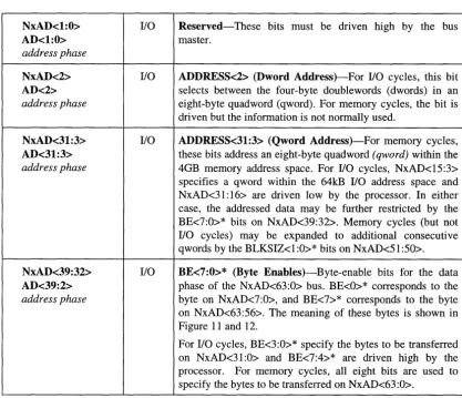
Address
c=
NxAD<1 :0> Reserved NxAD<2> Dword Address BitNxAD<31 :3> Qword Address
NxAD <63:0>
' - - - NxAD<39:32> Byte Enables (BE<7:0>*)
' - - - NxAD<45:40> Master ID (MID<5:0»
' - - - NxAD<46> Write or Read (W/R*)
' - - - NxAD<47> Data or Control (D/C*)
' - - - NxAD<48> Memory or 1/0 (M/IO*)
' - - - NxAD<49> Ownership Request (OWN*) ' - - - -_ _ _ NxAD<50> Reserved
' - - - NxAD<51> Block Size (BLKSIZ*)
' - - - - _ _ _ _ _ _ _ _ _ _ _ _ NxAD<55:52> Reserved
' - - - NxAD<56> Reserved
' - - - NxAD<57> Snoop Enable (SNPNBL)
L -_ _ _ _ _ _ _ _ _ _ _ _ _ _ NxAD<58> Cacheable (CACHBL)
NxAD<63:59> Reserved
Figure 10 NexBus/NexBus5 Address and Status Phase
[image:35.620.85.504.78.680.2]NexGen
lMNxAD<1:0> AD<1:0>
address phase
NxAD<2> AD<2>
address phase
NxAD<31:3> AD<31:3>
address phase
NxAD<39:32> AD<39:2>
address phase
PRELIMINARY
I/O
I/O
I/O
I/O
Nx586 Features and Signals
Reserved-These bits must be driven high by the bus master.
ADDRESS<2> (Dword Address)-For I/O cycles, this bit selects between the four-byte doublewords (dwords) in an eight-byte quadword (qword). For memory cycles, the bit is driven but the information is not normally used.
ADDRESS<31:3> (Qword Address)-For memory cycles, these bits address an eight-byte quadword (qword) within the 4GB memory address space. For I/O cycles, NxAD<15:3> specifies a qword within the 64kB I/O address space and NxAD<31: 16> are driven low by the processor. In either case, the addressed data may be further restricted by the BE<7:0>* bits on NxAD<39:32>. Memory cycles (but not I/O cycles) may be expanded to additional consecutive qwords by the BLKSIZ<I:0>* bits on NxAD<