Dynamic structural colour in thin film stacks and
patterned nanoparticle arrays
A PhD Thesis
by:
Keith Mark Wilson
Supervisor:
Prof. Louise Bradley
School of Physics Trinity College Dublin
i
Declaration
I declare that this thesis has not been submitted as an exercise for a degree at this or any other university and it is entirely my own work with the exception of assistance and collaboration recognised in the acknowledgements and throughout the thesis where applicable.
I agree to deposit this thesis in the University's open access institutional repository or allow the library to do so on my behalf, subject to Irish Copyright Legislation and Trinity College Library conditions of use and acknowledgement.
I have read and I understand the plagiarism provisions in the General Regulations of the University Calendar for the current year, found at http://www.tcd.ie/calendar.
I have also completed the Online Tutorial on avoiding plagiarism “Ready Steady Write”, located at http://tcd-ie.libguides.com/plagiarism/ready-steady-write.
iii
Abstract
In this thesis a number of metal nanostructures have been investigated for structural colour at sub-micron scales. These structures have utilised localised surface plasmon resonance (LSPR) to produce near-field interactions between components, generating sharp spectral features in reflectance. The use of phase change materials (PCMs) have also been investigated, for dynamic tuning of colour after fabrication of the structures, with a view towards display applications.
An aluminium nanodisc-nanohole array structure is explored for colour generation in reflection. The structure consists of a square dielectric pillar array, with aluminium coating the top of the pillar and the backreflector to produce the disc and hole components. Simulation is carried out by the finite-difference time-domain (FDTD) method, with varying geometry parameters to determine the colour gamut of the structure. The strong LSPR of the disc and hole interact in a Fano resonance condition, resulting in sharp spectral features in the visible region. A 5 mm square array with 400 nm pitch and 200 nm diameter pillars have been fabricated by electron beam lithography (EBL), with close correlation between simulated and measured spectra. A diffraction effect has been observed, following a first order diffraction profile with grating constant of 400 nm, consistent with this sample. The limited viewing angle presented by this structure leads research towards alternative materials, capable of colour generation at smaller dimensions.
iv
measuring 100 x 100 µm, of 150 nm diameter discs with a 300 nm pitch have been fabricated using EBL. Assessment of the polymer film by ellipsometry revealed that the fabrication process caused negligible damage, and good agreement is found between arrays simulated by FDTD and those fabricated.
A thin film stack consisting of layers of Indium Tin Oxide (ITO) with an intermediate Vanadium Oxide (VO2) layer with an Ag backreflector is explored for dynamic structural colour. Compared with other phase change materials (PCMs), such as Germanium Antimony Telluride (GST), VO2 can be considered as a lower power consumption alternative. It has been overlooked in the visible region, due to its smaller refractive index change below 700 nm. The sensitivity of the visible reflectance spectrum to the change in phase of a 30 nm VO2 layer is shown to increase after it is incorporated in a thin film stack, with comparable performance other phase change materials. An improved maximum ΔR is observed, with 20% recorded in structures containing GeSbTe (GST) and AgInSbTe (AIST) increasing to 30% in a 10-30-25-100 nm ITO-VO2-ITO-Ag thin film stack. CIE separation is also shown to increase in this VO2 stack configuration. Inclusion of a top ITO layer is also shown to improve the chromaticity change on phase transition.
v
Acknowledgements
First and foremost, I would like to thank my supervisor, Prof. Louise Bradley for the opportunity to undertake my PhD in her research group. Her advice and encouragement has been invaluable to my completion of this undertaking.
I would also like to thank the members of the research group, with whom I have spent much of my time working with over the last few years. In particularly Dr. Cristian Marocico, who has been mentored me in theory and simulation a great deal throughout the project, even after departure from the group.
I would also like to thank John Gough, a great friend and colleague, that has been instrumental to my success in the lab. My thanks also go to the other members of the group, Graham Murphy, Luke Higgins, Vasilios Karanikolas, Jorge Garcia, and Xia Zhang for their very helpful discussions.
Thanks are in order for the members of the wider research group, in particular Brian Jennings, David McCloskey, and Chris Smith for their expertise in the lab when issues arose. I must also thank Allan Bell, for his excellent training and help in fabrications of samples throughout the first two years.
My thanks to the extremely helpful and infinitely patient technicians in the workshop Dave Grouse and Pat Murphy for all the contraptions, and the ever wise and helpful IT wizards Ken Concannon and Alan O’Meara.
My friends, who have helped me get through the stressful patches.
A very special acknowledgement to my parents Mark and Karen, and sister Claire, who have always been supportive and encouraging in all my studies, and have helped me so much in this endeavour.
vi
List of Publications and Conference contributions
Publications
1. Graham P Murphy, John J. Gough, Luke J. Higgins, Vasilios D. Karanikolas,
Keith M. Wilson, and A Louise Bradley, “Ag colloids and arrays for plasmonic
non-radiative energy transfer from quantum dots to a quantum well”,
Nanotechnology 28(11), 115401 (2017).
2. Keith M. Wilson, Cristian A. Marocico, and A. Louise Bradley, “Dynamic structural colour using Vanadium Dioxide thin films”, J. Phys. D. Appl. Phys.
51(25), 2018.
3. Keith M. Wilson, Cristian A. Marocico, Chris Smith, and A. Louise Bradley,
“Hybrid metal nanostructure arrays for colour printing”, Manuscript submitted, Nanoscale, August 2018.
4. Keith M. Wilson, Cristian A. Marocico, Esteban Pedreuza, and A. Louise
Bradley, “Angular diffractive effects and structural colour in aluminium
plasmonic nanopillar array”, Manuscript in preparation, 2018.
Conference contributions
1. Keith M. Wilson and A. Louise Bradley. “Dynamic structural colour using Vanadium dioxide thin films”. Photonics Ireland 2017. 13th-15th September 2017, Galway, Ireland. (Poster)
2. Keith M. Wilson, Cristian A. Marocico, Esteban Pedreuza, Chris Smith, and A. Louise Bradley. “Hybrid metal nanostructure arrays for colour printing”.
ICTON 2016. 10nd-14th July 2016, Trento, Italy. (Oral presentation)
3. Keith M. Wilson, Cristian A. Marocico, and A. Louise Bradley. “Design of
metallic nanostructured arrays for display applications”. Photonics Ireland 2015.
vii
Contents
Declaration ... i
Abstract ... iii
Acknowledgements ... v
List of Publications and Conference contributions... vi
Contents ... vii
1 Motivation ... 1
2 Background ... 13
2.1 Thin films ... 14
2.1.1 Interference ... 14
2.1.2 Absorption ... 16
2.1.3 Phase Change Materials ... 19
2.2 Plasmons ... 22
2.2.2 Surface Plasmon Polaritons ... 23
2.2.3 Localised Surface Plasmon Resonance ... 26
2.3 Fano resonance ... 30
2.4 Array effects ... 32
2.4.1 Diffraction ... 32
2.5 Colour theory ... 34
2.5.1 CYMK ... 35
2.5.2 RGB ... 36
2.5.3 CIE ... 38
2.6 Conclusion ... 40
viii
3.1 Simulation ... 42
3.1.1 Transfer Matrix Method ... 42
3.1.2 Finite Difference Time Domain ... 45
3.1.3 Discrete Dipole ... 51
3.1.4 Refractive Index information ... 52
3.1.5 Colour conversion of spectra to sRGB and CIE xyY ... 52
3.2 Fabrication ... 56
3.2.1 Lithography ... 57
3.2.2 Resists and Development ... 60
3.2.3 Material Deposition ... 61
3.3 Characterisation ... 62
3.3.1 Structural parameters... 62
3.3.2 Normal incidence measurements ... 63
3.3.3 Angular measurements ... 65
3.4 Conclusion ... 66
4 Aluminium Nanostructure ... 67
4.1 Simulation ... 67
4.1.1 Validation ... 69
4.1.2 Al nanostructured array ... 72
4.1.3 Geometries ... 81
4.2 Experimental ... 89
4.2.1 Fabrication ... 89
4.2.2 Characterisation ... 90
4.2.3 Diffraction effects ... 94
ix
5 Hybrid Nanostructure ... 101
5.1 Simulation ... 102
5.1.1 Hybrid nanostructure array ... 103
5.1.2 Geometries ... 113
5.1.3 Material Composition ... 121
5.2 Experimental ... 124
5.2.1 Fabrication ... 124
5.2.2 Characterisation ... 126
5.3 Conclusion ... 131
6 VO2 thin films ... 133
6.1 Simulation ... 134
6.1.1 AIST and GST structures ... 134
6.1.2 Vanadium Oxide thin films ... 139
6.1.3 ITO-VO2-ITO stacks ... 142
6.1.4 VO2 Thickness ... 145
6.1.5 Impact of the ITO top contact ... 148
6.2 Conclusion ... 151
7 Metal nanoparticle-VO2 structures ... 153
7.1 Simulation ... 154
7.1.1 Hybrid structure with VO2 layer ... 155
7.1.2 Discs on VO2 ... 160
7.1.3 Particle shapes on VO2 ... 163
7.1.4 Discs imbedded in VO2 ... 170
7.1.5 Particle shapes imbedded in VO2 ... 175
x
8 Conclusion ... 181
Summary ... 181
Outlook ... 185
Appendix A ... 187
Appendix B ... 195
Appendix C... 197
1
Chapter 1
Motivation
The human eye is a wonder of nature that grants the most information-packed sense of all; colour vision. Over the past 30 years, huge leaps have been made in display technology, from the very earliest in the form of cathode ray tubes (CRTs) [1], to the incredibly high resolution and high contrast organic light emitting diode (OLED)[2] displays. With the advent of mobile devices that are becoming more powerful and power-hungry, the battery technology that powers these devices struggles to keep up[3]. Focus has shifted towards low-power display technology for mobile phones and tablets, as developments are made to provide lower cost alternatives to the active displays used across most technologies. The implementation of passive displays is in its infancy[4], with much improvement required before widespread adoption of these systems can be achieved.
Figure 1.1: Butterfly wings exhibiting structural colour due to the dimensions of the
chitinous ridges on the wing surface. For species (a) Ornithoptera Croesus, and (b)
Ornithoptera priamus.
2
by light absorption in the molecular bonds for certain bands of the visible region, as seen in Figure 1.2. Structural colour allows for the printing of colour at and below the optical diffraction limit[5–7], without the use of dyes/pigments.
Figure 1.2: (a) Chlorophyll C2 molecule commonly found in plants. (b) Leaf absorbing
red and blue wavelength regions, reflecting green light.
This technology is becoming more attractive commercially, as improvements to lithographic processes[8,9] become more widely available and scalable. Structural colour has been demonstrated in randomly distributed nanoparticle[10], and lithographically patterned nanostructures[6,11,12]. These metallic nanostructures have a number of advantages over dielectric structures, such as narrow spectral features, and smaller geometry requirements. The primary advantages of metallic structural colour technologies over traditional dye-based colour generation methods are that these nanostructure architectures are resistant to photo-bleaching[4], exhibit high robustness to physical stresses[13], the colour response of the structure can be generated at sub-diffraction dimensions[5–7]. Sub-diffraction limit nanostructures can generate structural colour by manipulating light on the nano-scale.
3 These aspects indicate that metal nanostructures can be a viable technology to be used in future devices, in areas such as colour printing[11,20], holograms[21,22], display technology[23], as well as surface enhanced Raman scattering (SERS)[24], and anti-counterfeit measures[25] due to the difficulty in recreating nanostructured devices, and the particular spectral response they generate.
Thin film structures are applied across the field of optics for anti-reflection coatings, high reflection mirrors and optical filters. These structures can be as simple as a couple of layers of different materials or complex multi-layer aperiodic stacks. There are many examples of thin film structures producing vibrant structural colour across the visible wavelength range[26,27]. These structures exploit the interference of electromagnetic waves reflected at the interfaces. Traditionally, structures have been fabricated using lossless materials[28] to exploit the interference effect, though investigations have been carried out with highly absorbing materials[27,29]. Designs for high reflectance structures often incorporate a back metallic film[26]. More recently, very simple structures formed using a few nanometre thick highly absorbing layer of Ge deposited on an optically thick Au layer have been considered for coloured optical coatings[26]. It was shown that for a sufficiently thin Ge film interference effects could persist, and the desired reflected colour can be selected by varying the thickness of the ultrathin Ge layer, as shown in Figure 1.3.
Figure 1.3: Nanometre optical coatings based on strong interference effects in highly
absorbing media[26]. Strutural colour, with variation achieved by changing Ge
4
[image:16.595.92.458.404.629.2]Thin film stack structures capable of structural colour have been demonstrated by the formation of optical cavities in metal-insulator-metal (MIM) thin film stacks[30], with strong interference effects causing particular wavelengths to be constructively and deconstructively interfered, resulting in portions of the visible region being selectively reflected back to the observer. Other structures have utilised highly absorbing materials[26] to absorb certain wavelength ranges of the visible region, and produce coloured films with much thinner materials. However, these structures are material limited, and colours palettes are often incomplete as a product of restricted variables available that determine the colour produced. As illustrated in Figure 1.4, randomly distributed nanoparticle arrays have been demonstrated as strong colour filters[10], while maintaining ease of fabrication due to simple techniques of deposition. However, these materials are limited by the random distribution of nanoparticles resulting in broad resonance features, and so colour clarity of the structures is low.
Figure 1.4: Angle-insensitive plasmonic color filters with randomly distributed silver
nanodiscs[10]. This structure consists of randomly distributed Ag nanodiscs of different
sizes on a SiO2 substrate.
5 particularly apparent with noble metals, which produce strong plasmon responses[31,32]. Though it is important when utilising materials such as Ag, that encapsulation occurs immediately after Ag deposition to prevent tarnishing[33]. MIM nanoparticle arrays have been extensively studied in the Near-IR[34,35], though they consist of a single metal composition in both the nanoparticle array and backreflector components. Such structures have also been shown produced varied colour palettes, with uniform arrays of nanoparticles[6,20], mixed unit cells[11] to improve control over the colours produced, and non-circular particles to induce polarisation dependencies[12,36,37]. Though these structures hold difficulties in scalability to a mass production, progress has been made in recent years in nanoimprint lithography (NIL)[38,39], and in extreme ultraviolet lithography (EUV)[8], with wavelengths in the range of 10-14 nm facilitating the production of sub-diffraction limited geometries optically.
6
arrays, there has been some investigation. In the work by Clausen et al.[58], the plasmon resonance hybridization resulting of disk/hole coupled plasmonic modes has a major impact in the reflectance spectra. In the work by Duempelmann et al.[59], Al nanowires in a grating substrate generate plasmonic modes, that interact with surface plasmons to generate angular dependent colour.
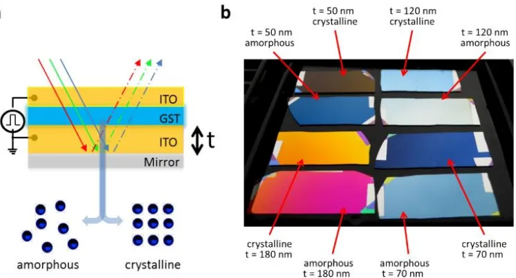
7 Figure 1.5: An optoelectronic framework enabled by low-dimensional phase-change
films[72]. This structure consists a GST thin layer between two layers of ITO, with a Pt
backreflector. Colour change is induced upon phase transition of the GST.
While these materials offer many advantages, they pose toxicity concerns[77] and, due to their high absorption, very thin layers are required. For example, in the case of GST layers as thin as 7 nm are required, introducing difficulties for the uniform fabrication of such ultra-thin layers[72].
[image:19.595.134.507.54.255.2]8
The refractive index change of VO2 is greatest in the infra-red and microwave spectral ranges, which has motivated extensive studies using VO2 for applications in IR waveguides[19,84,85], optical communications[83,86,87], IR sensing[88,89], and many THz applications[84,90,91]. It has also been widely studied for thermochromic windows[92] and, more recently, has been attracting renewed interest for tunable metasurfaces in the IR[93–95]. An ultra-thin layer of VO2 on a sapphire substrate has been used to demonstrate a thermally tunable perfect absorber in the IR[96]. The material exhibits a smaller but still significant complex refractive index change in the range below 700 nm[17]. The phase transition produces a maximum change of 60% in n and of 20% in κ across the visible spectral range. While, this is lower than that of other PCMs, such as GST with a maximum change of 100% in n and 250% in κ over the same spectral range, the advantages of VO2 described above warrant consideration of its potential for applications in the visible wavelength region. A previous study of VO2 layers of varying thickness deposited on quartz showed that in the visible region the transmittance of the semiconductor phase is generally lower than that of the metallic phase for film thicknesses less than 35 nm but for thicker films the transmittance of the insulating phase is greater, arising from interference effects[97]. However, this study considered only a single layer of VO2 on a substrate. Increased sensitivity to the refractive index change in a VO2 layer over the visible range can potentially be increased by using multilayer structures comprised of transparent dielectric materials and VO2 layers on a reflective back-reflector. In this thesis, the extent to which the tuning of the reflectance spectra can be exploited for colour switching is investigated.
9 utilised extensively in these nanoparticle systems[100], with significant alteration of the LSPR observed in the visible[101,102]. Applications of these structures in the visible region have focused on light harvesting[16,102] and sensing[18] applications. In the case of VO2-nanoparticle systems, colour generation[103] and sensing in the visible[104] have been investigated. However, research has focused on the large refractive index change of VO2 in the IR region[105–107], with often limited change observed in the visible when included. For this reason, many efforts with nanoparticle arrays have been in the IR[108]; in memory[109], optical switches[110–112], and sensing[113]. Patterning on-top of VO2 with e-beam lithography[103,111] has been achieved without damage of the crystalline structure. In brief, this thesis investigates a number of nanostructures in the generation of structural colour, with an emphasis on dynamic colour in later chapters. The plasmonic architectures under consideration include a low-cost Aluminium-based nanodisc array structure, as well as a hybrid Au-Ag structure that constitutes a smaller footprint, both of which are capable of producing vibrant colour in reflection. VO2 PCM structures are first introduced in a thin film stack design, with the goal of maximising the sensitivity of the VO2 in the visible. Finally, nanoparticles are incorporated into the structure to avail of the sensitive LSPR phenomenon. In this way, dynamic structural colour is achievable after fabrication of the nanostructures.
10
The methods of simulation, fabrication, and characterisation will be the focus of
Chapter 3. In particular, the introduction of the transfer matrix method (TMM), and finite-different time-domain (FDTD) simulations techniques are discussed. The methods of material deposition are presented, and the systems for electron beam lithography (EBL) are briefly reported. The in-house optical characterisation setup is outlined in this chapter, as well as the various other characterisation techniques utilised throughout the thesis.
A patterned plasmonic aluminium nanostructure is the first to be investigated for the generation of structural colour and is the focus of Chapter 4. This architecture is of a similar configuration to previous literature designs[11], and consists of an array of dielectric pillars, with Aluminium on the backreflector surface, and top of the discs. This creates a structure with a disc and hole component, separated by the dielectric pillar by tens of nanometres, allowing for strong interaction between the components. The primary goal of this chapter to validate the simulation techniques, and to be a proof of concept for fabrication of low costs patterned nanoparticle arrays in the facilities available.
In Chapter 5 a hybrid metal nanostructure consisting of Au discs on a polymer thin film and Ag backreflector is investigated, due to the limitations associated with the structure investigated in Chapter 4. The structure benefits from the strong LSPR of Au nanodiscs, high reflectivity of Ag and the optical cavity produced by the transparent polymer layer, while maintaining a smaller unit cell footprint than the Aluminium structure. This minimises angular dependencies of the structure, with regards to diffractive effects, allowing for wide viewing angles.
11
Chapter 7 follows on from the thin film design proposed in Chapter 6, and incorporates Au nanoparticles of varying size and shape. The LSPR response and electric field distribution surrounding these particles are highly dependent on size, shape, and surrounding media; the nanoparticles act as sensitive components in the structure that further increase the colour change potential of the structure upon phase transition.
13
Chapter 2
Background
Summary
This chapter will address the main background theory associated with the experimental sections of the thesis. As this thesis has focused on structural colour generated by a series of nanostructure designs, from thin film stacks to patterned nanoparticle arrays, these are the main topics addressed. Thin film stacks are one of the simplest forms of assemblies capable of structural colour. There are two primary mechanisms by which thin films selectively filter light of certain wavelength ranges to generate colour in reflectance; interference, and absorption. The basis for these mechanisms are first introduced. The concept and mechanism of Phase Change Materials are also presented briefly.
Nanoparticle arrays filter light via absorption and scattering by particles on the order of the wavelength incident on the structure, as well as interference mechanisms. Light incident on a dielectric-metallic surface or interface may induce oscillations of conduction band electrons in the metal if the momentum of the propagating wave and surface oscillation can be matched. These oscillations are known as a surface plasmons, and are in part, due to the dissociated electron cloud in the metal. The reflectance/transmittance spectra in plasmonic systems are highly wavelength dependent, with distinct absorption and scattering bands. As the wavelength range of visible light is in the 400-700 nm region, these structures can also result in angular diffraction effects due to their sub-micron scales, and are introduced here.
14
2.1
Thin films
Thin films can be considered the simplest structure capable of generating structural colour. They consist of one or more layers of materials, coating the entire surface of a substrate. These layers can be dielectric or metallic, and can range from only a few nanometers thick, to several microns. Here, the primary mechanisms are described by which these stacks can selectively absorb incident light, and in doing so, appear coloured in reflection or transmission.
2.1.1
Interference
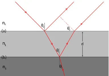
Propagating light is a transverse electromagnetic wave, with electric and magnetic fields oscillating orthogonal to each other and the propagation vector. Optical interference is a phenomenon in which propagating light waves interact with each other, as a superposition of the electromagnetic waves is formed. Depending on the phase difference between these waves, which may result in constructive or deconstructive interference. This phase difference can be induced in reflection from two interfaces of a layered structure, separated a distance d, with an example presented in Figure 2.1.
Figure 2.1: Schematic of a structure exhibiting thin film interference, with n0 as the
[image:26.595.85.469.457.725.2]15 The refractive index a material (n) is the measure of the difference in velocity that light propagates through the material (v), compared to that of propagation in free space (c), as n = c/v. In the case shown in Figure 2.1, assume that n0 = 1, and that n0 <
n1 < ns. When light is reflected at a boundary in which the refractive index is higher,
there is a 1800 phase shift in the reflected light[114]. Here, this occurs at both boundaries, as n is higher at the far side of the boundary in both cases. Constructive interference will occur when the optical path length difference between the two waves is equal to a multiple of the wavelength of incident light, λ, as[114]:
2𝑛1𝑑𝑐𝑜𝑠(𝜃1) = 𝑚𝜆 (2.1)
where n1 is the refractive index of the layer, θ1 is the angle of the incident wave on
the lower boundary, m is an integer multiple. This is only the case in the case if n1 <
ns, as there will be a phase shift induced upon reflection at both interfaces. In the
case of n1 > ns, the dependency follows:
2𝑛1𝑑𝑐𝑜𝑠(𝜃1) = (𝑚 −
1
2)𝜆 (2.2)
As no phase shift is induced at the lower boundary, a correction term of -1/2 is included. The relationship between the angle of the incident wave (θ0), and the
angle of incidence at the lower boundary (θ1) is described by Snell’s law as[115]:
𝑛0𝑠𝑖𝑛(𝜃0) = 𝑛1𝑠𝑖𝑛(𝜃1) (2.3)
where n0 is the incident refractive index, usually air (n = 1), and n1 is the refractive
index of the layer. It is clear that the optical path length is highly dependent on the angle of incidence of the light, and so thin film interference is a phenomenon highly dependent on illumination and observation angle.
16
wavelength of light in order to satisfy the integer multiple condition in the optical path length.
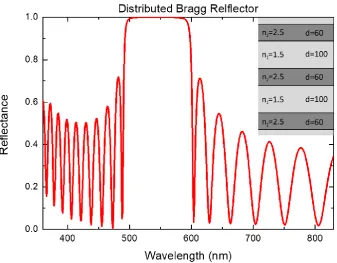
This is the principle operation of the distributed Bragg reflector (DBR), a structure formed from multiple layers of alternating dielectric materials with thickness on the order of a quarter of the wavelength. Constructive interference will occur according to Equation 2.2, due to the alternating n values. Each layer in the stack partially reflects the light, with the optical path difference resulting in a first order (m = 1) constructive interference when d = λm/4, where λm is the wavelength of light in the
material (λm= nλ). The region of high reflectance formed by this structure is called
the photonic stopband, an example of which is presented in Figure 2.2.
Figure 2.2: Reflectance spectrum of a 20-layer Distributed Bragg Reflector with 10
alternating layers of n1 = 1.5 and n2= 2.5 on a Si substrate, with layer thickness (d) of 100
nm and 60 nm, respectively. This is calculated by the Transfer Matrix Method, with a
stop band of approximately 100 nm in the 500-600 nm region of the visible spectrum.
(Inset) Schematic of layered structure.
2.1.2
Absorption
[image:28.595.110.448.313.576.2]17 scattering in the material transfers energy to the ion cores, in the case of crystals, or to the vibration of bonds in molecules. Photons are absorbed when resonant with an electron energy level transition, or above the band gap of the material. This absorption of energy excites an electron to a higher energy level. The electron can then fall back to its ground state, in which case a photon is re-emitted, or the energy can be lost via non-radiative recombination of the electron to the ground state. This energy in the latter case is usually converted to heat. Studies into using thin metallic films for colour generation[27] have successfully generated vibrant colours from thin films of Ge on Au[26], with colour varied by changing the thickness of the Ge film.
The real part of the refractive index of a material (n) has been previously stated, though there also may be an imaginary component (κ), known as the extinction co-efficient, responsible for describing the light attenuating characteristics of a material. In dispersive media with a complex refractive index, these values vary by frequency (ω), as the material responds to the electromagnetic wave differently depending of the frequency of oscillation. The larger the κ value, the more lossy the material is at that particular wavelength. Permittivity (𝜀̅) is the resistance to the formation of an electric field in a material, and related to the frequency dependent complex refractive index (𝑛̅) as[116,117]:
𝜀̅ = 𝜀′ + 𝑖𝜀′′ = 𝑛̅2 = (𝑛 + 𝑖𝜅)2 (2.4)
where
𝜀′ = 𝑛2− 𝜅2 (2.5a)
𝜀′′ = 2𝑛𝜅 (2.5b)
and
𝑛 = √|𝜀̅| + 𝜀′
2 (2.6a)
𝑘 = √|𝜀̅| − 𝜀′
18
Transparent materials, such as glass or other dielectric materials, allow light below a certain frequency to pass through, as the first excited energy level of electrons in the material is larger than the energy of the incident photon below that frequency. The photon does not interact with the electrons in the material, and so light passes through without being attenuated. These materials are described by a refractive index which has a small extinction coefficient (κ).
Metals have a dissociated electron gas shared throughout the material. This is due to the position of the Fermi level in the conduction band in the material. The Fermi level is the highest energy level of an occupied electron orbital, and its position in the conduction band allows electrons to be removed from their ion cores easily by an applied electric field. This electron gas cloud is highly mobile, and can respond to the incident electromagnetic field below a certain frequency, known as the plasma frequency. The plasma frequency (ωp) is described by[116]:
𝜔𝑝 = √𝑛𝑒𝑒
2
𝑚∗𝜀 0
(2.7)
where ne is the electron density, e is electron charge, m* is the effective mass of the
electrons, and ε0 is the permittivity of free space. From Equation 2.7, it can be seen
that for different metals, the most important parameter when concerning the plasma frequency is electron density in the metal.
Figure 2.3: Real (n) and imaginary (κ) parts of the refractive index of a generic metal as
19 Above the plasma frequency, electrons are not able to respond to the driving oscillating field completely, due to inertia, resulting in a resistance of the material to the formation of an electric field. As a result, the material becomes transparent to light. Depending on the complex refractive index of the metal, it may absorb light according to the imaginary (κ) component. For most metals, this plasma frequency occurs in the ultra-violet region, and they appear to reflect the entire visible region.
However, for some metals such as Cu, Ag, and Au, often referred to as “noble”
metals, each have a filled 3d, 4d, and 5d electron orbital shell, but only a single electron in the 4s, 5s, and 6s shell, respectively[119]. This allows for inter-band transitions, where electrons are excited from the core electron orbitals, altering the refractive index significantly. In the case of Au and Cu, this leads to high reflectance at only the longer wavelengths of the visible, resulting in their red/orange hues. In the case of Ag this occurs at higher frequency leading high reflectance in the visible, with a near-UV transparency[120].
2.1.3
Phase Change Materials
20
“transition” temperature, or as an electric field is applied to the material, to induce structural changes by Joule heating[18][121].
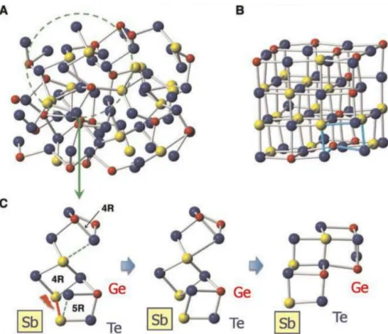
Figure 2.4: Crystalline structure of GeSbTe in the (A) low temperature amorphous
insulating phase, and (B) high temperature crystalline metallic phase. (C) Cutout of the
larger structure, illustrating the structural change[122].
[image:32.595.139.412.109.344.2]VO2 is a solid-solid PCM that transitions from a low temperature semiconducting monoclinic phase to a high temperature rutile metallic phase at 680C[17], significantly lower than the 1450C required for GST[67].
Figure 2.5: Temperature vs Resistivity plot for VO2, with inset of VO2 structure in the
[image:32.595.134.419.495.726.2]21 In the monoclinic phase, the crystalline unit cell of VO2 contains a V4+-V4+ pair along the c-axis of the crystal[124]. Above the transition temperature, the c-axis pairs dissociate, closing the gap in the conduction band for vanadium in the 3d orbital[125], placing the Fermi level in the d orbital, and allowing for high conductivity, as shown in Figure 2.6.
Figure 2.6: Band structure of VO2 in the low temperature insulating phase, and high
temperature metallic phase. [126,127]. The d∥ band is due to V-V pairs in the c-axis, as
a result of the overlap of the dx2-y2 orbital in Vanadium.
22
index change of VO2 is greatest in the infra-red and microwave spectral ranges, which has motivated extensive studies using VO2 for applications in IR waveguides [19,84,85], optical communications [83,86,87], IR sensing [88,89], and many THz applications[84,90,93]. The material exhibits a smaller but still significant complex refractive index change in the range below 700 nm[17], and with lower power consumption than for AIST or GST. This makes the material a viable alternative in the visible region, provided that the limited refractive index change can be utilised to its best potential.
2.2
Plasmons
Plasmons are oscillations of the conduction band electrons at the interface between materials in which there is a change in sign of the dielectric permittivity, ε. Metals exhibit negative relative permittivity at optical frequencies below the plasma frequency, where the electrons can respond completely to the induced field of the incident wave. The negative permittivity of metals below the plasma frequency is the origin of the high reflectivity observed in the visible, as most metals present plasma frequencies in the UV[116].
Plasmons can form at the boundary between a dielectric (d) and metal (m) material, though it can also occur at the boundary between a metal and air, or vacuum, due to their positive permittivity. However, as the plasmon has a higher energy than the propagating wave, it must be coupled to the interface. This can be done by utilising defect sites, or coupling into a material with higher refractive index to overcome the momentum mismatch. The plasmon has a shorter wavelength than the free-space or bulk propagating wave, it exhibits significant spatial confinement, and large field localisation.
23
2.2.2
Surface Plasmon Polaritons
Surface Plasmon Polaritons (SPPs) are propagating longitudinal surface waves that occur along the dielectric-metal interface. These present as evanescent fields perpendicular to the surface, that decay rapidly into the dielectric and metal, as illustrated in Figure 2.7.
Figure 2.7: Surface plasmon polariton (SPP) oscillation at a dielectric-metal interface. A
decaying evanescent field is observed normal to the surface[128].
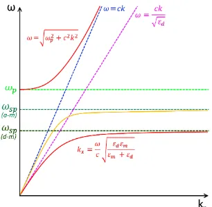
The dispersion relation of a propagating oscillating light wave is the relationship between its frequency (ω) and wavevector (κ). The dispersion relation for a propagating wave in a non-dispersive dielectric medium is[116]:
𝜔 = 𝑐𝑘
√𝜀𝑑
(2.8) where c is the speed of light, and the wavenumber is:
𝑘 =2𝜋
𝜆 (2.9)
The dispersion relation for the bulk plasmon in a metal is:
𝜔 = √𝜔𝑝2+ 𝑐2𝑘2 (2.10)
24
Figure 2.8: Dispersion relation of SPPs, at an air-metal (a-m) and dielectric-metal (d-m)
interface. The blue and pink light lines are the relations for free space, and dielectric
media, respectively.
Where ωp is the plasma frequency of the metal, and is described in Equation 2.7.
This relation is asymptotic, and tends towards the free space light line as kx
increases.
Surface plasmons can be excited at a dielectric-metal interface below the plasma frequency, in a regime where there is no propagation into the medium can occur, asvvalues are imaginary. Only evanescent fields are supported at the interface between the dielectric and metal.
The wavevector along the propagation direction (kx) is also asymptotic as it
approaches the surface plasmon frequency (ωsp), and is described by:
𝑘𝑥 =𝜔
𝑐 √
𝜀𝑑𝜀𝑚
𝜀𝑚 + 𝜀𝑑 (2.11)
From this, it can be determined that the maximum kx occurs where εd = -εm. This
25
𝜀𝑚 = 1 −𝜔 𝑝
2
𝜔2 (2.12)
Therefore, the characteristic angular frequency of the plasmon that can be supported at the metal-dielectric interface is described by:
𝜔𝑠𝑝 = 𝜔𝑝
√1 + 𝜀𝑑 (2.13)
It is clear that the angular frequency is highly sensitive to the permittivity of the dielectric at the interface. In the case of a metal-air interface, where εair = 1, this
relationship simplifies to:
𝜔𝑠𝑝 = 𝜔𝑝
√2 (2.14)
For the wavevector in the z direction, perpendicular to the interface, in the metal and dielectric:
𝑘𝑧𝑚2 = 𝑘
𝑥2− 𝜀𝑚 (
𝜔 𝑐)
2
(2.15a)
𝑘𝑧𝑑2 = 𝑘𝑥2− 𝜀 𝑚 (
𝜔 𝑐) 2 (2.15b) where 𝑘𝑧𝑚 𝑘𝑧𝑑
= −𝜀𝑚
𝜀𝑑 (2.16)
SPPs can propagate for tens of microns depending on the losses at the interface[129]. As the SPP is an evanescent wave that decays quickly into both media, the SPP is not directly observed as the oscillation is confined to the surface interface, and far-field radiation of the light is often only measurable due to defect sites on the surface[130]. Surface near-field optical microscopy (SNOM) may be used to probe the near-field very close to the interface[129] to measure SPP characteristics.
26
the effective wavelength of the PSP, scattering can lead to the formation of standing waves, which results in a surface plasmon stop-band[131]. In the case of square arrays, where the periodicity is in both directions, this can lead to a full stop-band gap forming for surface plasmons[131,132]. This stop-band can affect the reflectance response of the nanostructure in the far-field in a narrow wavelength range. The wavelength (λPSP) of the PSP formed by the periodic array can be found
by[51,133,134]:
𝜆𝑃𝑆𝑃 = 𝑃
√𝑖2+ 𝑗2√
𝜀𝑑𝜀𝑚
𝜀𝑚 + 𝜀𝑑 (2.17)
where P is the pitch of the nanoparticle array, and the scattering orders are denoted by the integers i and j.
2.2.3
Localised Surface Plasmon Resonance
LSPR is a non-propagating form of plasmon excitation which occurs in conduction band electrons of metal nanoparticles. Incident electromagnetic radiation is coupled to these particles, often smaller than the wavelength, and induces the electrons in the conduction band to oscillate in response. As the electrons move across the surface, they are confined by the boundaries of the particle, as shown in Figure 2.9. These coherent plasmon oscillations are greatest at a resonant frequency defined by the size, shape, material and surrounding refractive index.
Figure 2.9: Localised Surface Plasmon Resonance (LSPR) oscillation in metal
nanoparticles, induced by the incident oscillating field. Conduction band electrons react
to the incident field by moving across the surface, producing strong field
27 The simplest particle can be examined; a sphere, using the quasi-static approximation provided that the size (d) is smaller than the wavelength (λ) of incident light. In this regime, the phase of the oscillating field across the particle can be assumed to be constant, and the field distribution can be calculated by simplifying to a particle in an electrostatic field. The dipole moment (Ρ) of the nanoparticle induced by the external field (E0) can be described by[116]:
𝛲 = 𝜀𝑑𝜀0𝛼𝐸0 (2.18)
where α is the polarizability of the particle. This is defined as[116]:
𝛼 = 4𝜋𝑎3 𝜀𝑚− 𝜀𝑑
𝜀𝑚 + 2𝜀𝑑 (2.19)
Here, a is the radius of the sphere. This follows the Clausius-Mossotti relation for molecular polarizability[135]. An interesting dependency is revealed there, in that the maximum polarizability of the particle occurs when εm = -2εd, known as the
Fröhlich condition[136]. This is the maximum dipole excitation experienced by the metal nanoparticle, or the localised surface plasmon resonance (LSPR). Large field enhancement is experienced in close proximity to the particle in the frequency region of highest polarizability.
From this relation, the cross-section of extinction (CExt) can be determined. This is
the effective area of collision in the interaction between the incident field and particle. The extinction is the combination of scattering (CSca) and absorption (CAbs)
cross-sections, due to the particle as:
𝐶𝐸𝑥𝑡 = 𝐶𝐴𝑏𝑠+ 𝐶𝑆𝑐𝑎 (2.20)
The dependencies of CAbs and CSca follow the form[116,137]:
𝐶𝐴𝑏𝑠 = 𝑘 𝐼𝑚[𝛼] = 4𝜋𝑘𝑎3 𝐼𝑚 [𝜀𝑚− 𝜀𝑑
𝜀𝑚 + 2𝜀𝑑] (2.21a)
𝐶𝑆𝑐𝑎 =
𝑘 6𝜋
4
|𝛼|2 = 8𝜋
3 𝑘
4𝑎6 |𝜀𝑚− 𝜀𝑑
𝜀𝑚 + 2𝜀𝑑
|
2
28
nanoparticle in a refractive index material of n = 1.33 is shown in Figure 2.10 (a) for absorption cross-section and (b) for scattering cross-section.
Figure 2.10: (a) Absorption and (b) Scattering cross-section spectra for Ag nanoparticles
of 10-100 nm in 10 nm steps. Refractive index of the surrounding media is n = 1.33[138].
It is important to note the scaling of absorption and scattering, where the a3
dependency is dominant in small particles, but is quickly eclipsed by the scattering cross section, scaling with a6. As such, the measurement of scattering from small
particles is difficult to examine in the presence of larger scattering particles, and so rely on absorption measurements, with a smaller scaling factor of a3[139], which is
demonstrated in Figure 2.10 (a).
Using the relation in Equation 2.20, and the dependencies revealed in Equation 2.21a and 2.21b, the extinction cross-section for a sphere of volume (V), follows as[116]:
𝐶𝐸𝑥𝑡 = 9𝑘𝜀𝑑 3
2𝑉 𝐼𝑚 𝜀𝑚
′′
[𝜀𝑚′ + 2𝜀
𝑑] + (𝜀𝑚′′)2
29 Figure 2.11: (a) Extinction cross-section spectra for Ag nanoparticles of 10-100 nm in 10
nm steps. Refractive index (n) of the surrounding media is 1.33. (b) Extinction
cross-section of 50 nm particles in varying refractive index media, from n = 1 to 1.923[138].
Figure 2.11 (a) reveals that the extinction red-shifts, and increases in intensity as the diameter of the Ag nanoparticles are increased. Shown, in Figure 2.11 (b), is the extinction cross-section for 50 nm spherical Ag particles in varying refractive indices. This illustrates that the peak position is highly sensitive to the refractive index of the surrounding media, and red-shifts significantly as the refractive index increases. The extinction determines the total energy of the incident wave that is lost due to interaction with the particle, as:
1 = 𝑇 + 𝑅 + 𝐸𝑥𝑡 = 𝑇 + 𝑅 + 𝐴𝑏𝑠 + 𝑆𝑐𝑎 (2.23)
where transmission (T) and reflection (R) can be collected in the far field. Absorption (Abs) cannot be collected, and is lost in the material. Scattered (Sca) light can be collected, but has a large angular dependency.
30
2.3
Fano resonance
While sharp spectral features in patterned nanostructures can be formed due to the relative uniformity in shape and periodicity of nanoparticles, another coupling mechanism for strong resonance responses in some patterned nanostructures is the formation of an interference effect known as Fano resonance[141–143]. This optical Fano resonance can be generated by the interference between components of a nanostructure, as the narrow discrete response generated by one component interacts with the broad continuum response from another, where the energy ranges of both components has an overlap. For example, where the evanescent field formed by the LSPR of a nanoparticle interacts directly with reflected light from another component[144,145], a Fano resonance can be formed. This is due to the LSPR forming a quantised oscillation of the conduction band electrons. These oscillations are confined by the boundaries of the material, and form an evanescent field in close proximity to the particle with a narrow frequency band. This evanescent field interacts with the broadband response formed by another component of the structure, such as the reflectance from a surface.
Figure 2.12: Coupled oscillator system that exhibits fano resonance lineshape as a result
of the driven oscillation of one affecting the oscillation of the other.[142]
31 separation in position of the peak amplitudes of the oscillators, and the driven amplitude. Critically, Fano resonance occurs in coupled oscillating systems in which the resonance is not identical in both oscillators and is observed where a broad resonance of one oscillator interacts with the narrow resonance of another, where the energy bands of the two systems are close or overlapping. This distinguishes Fano resonance from other coupled systems in which strong or weak coupled oscillation also occurs.
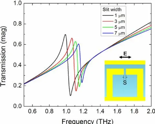
Figure 2.13: Fano resonance line shape in transmission as a function of slit width.
Nanostructure of metallic slit array on a quartz substrate.[146] (Inset) unit cell of
structure.
[image:43.595.185.453.235.450.2]32
the LSPR from Al nanodiscs interacting with a dielectric substrate interact form a Fano resonance response.
In the Aluminium nanostructure discussed later, it is noted that the colour generation is not simply due to a combination of reflectance from the LSPR of the disc array combining with the high reflectivity of the backreflector, but is due to a strong Fano resonance between components of the structures. In this structure, the LSPR of the discs forms evanescent fields that decay quickly away from the nanoparticle boundaries and acts as a quantised energy oscillation. This then interacts with the hole component, which has a much broader spectral response that overlaps with the energy band of the disc LSPR. When these components interact, they exhibit a strong Fano resonance.
2.4
Array effects
Diffraction is an interference effect that arises from the superposition of waves originating from coherence sources. Diffraction is observed in the structure examined in Chapter 4, formed by the array periodicity producing a diffraction grating, as the pillars act as scattering sites. Here, diffraction from an array is described.
2.4.1
Diffraction
33 resulting in a maximum intensity of light at that wavelength, at that angle, as demonstrated in Figure 2.14.
Figure 2.14: Schematic of a structure exhibiting diffraction interference, with incident
light scattered at each site, the path length difference marked in purple. Constructive
interference occurs where this path difference (d sinθ - d sinφ) is equal to mλ.
As the diffraction is occurring in reflection, from a surface with scattering sites, the path length differences between each scattering site are subtracted from one another to determine the angles of constructive interference. Maxima for each wavelength occurs at different collection angles (φ), as the integer multiple depends on the wavelength. This relationship can be described by[149]:
𝑠𝑖𝑛𝜃 − 𝑠𝑖𝑛𝜑 = 𝑚𝜆
𝑑 (2.24)
This allows for the formation of orders of diffraction, with m=0, ±1, ±2, ±3…
signifying the zeroth, first, second and third positive and negative orders, respectively. In the case of diffraction through a grating in transmission, the path length difference is determined by the addition of the terms.
Array structures have exhibited effects in normal reflectance, formed by diffraction parallel to the grating or array interface, known as a Wood’s anomaly
(WA)[51,150,151]. The wavelength at which these WAs occur at can be found by[51,150]:
𝜆𝑊𝐴 = 𝑃
34
where P is the pitch of the grating or nanoparticle array, and the diffraction orders are denoted by the integers i and j.
2.5
Colour theory
Human vision is determined by photosensitive receptors positioned at the back of the human eye, called the retina, onto which light is focused by the cornea. In low
light conditions, the photoreceptor responsible for vision is the “rod” cell, which is
extremely sensitive. At medium and high lighting conditions, rods are quickly
desensitised, and vision is determined by “cone” cells. There are three types of cone
cells, each responsible for light detection at different wavelengths. The colour cones responsible for human colour vision are the short (blue), middle (green) and long (red) wavelength photoreceptors, representing peak sensitivities at 400-420 nm, 530-540 nm and 560-580 nm respectively, though their sensitivity curves overlap significantly[152]. Signals from these cells are transmitted to the brain, where they are combined and are the basis for our sense of colour and vision.
When examining colours, two terms are often used to determine the characteristics of the response; luminance and chromaticity. Luminance is a measure of luminous spectral intensity, an indicator of the luminous power that is detected by an observer of an object or surface in reflection[152,153]. The larger the luminance value of the colour, the higher the visibility of that colour under the observation conditions. Methods for the determination of luminance will be described in Chapter 3, in Section 3.1.5.
Chromaticity is an objective quantitative measure of the quality of colour, and is independent of the luminance value of the object or surface being observed[152,153]. Chromaticity values denote every distinguishing colour that can be perceived by human vision. It can be subdivided into the classification of Hue and Saturation. Hue illustrates the “type” of distinguishable colour observed, such
35
“purity” of the colour observed, with white light considered the condition of lowest
colour saturation, and the primary colours of red, green, and blue as the highest. There are many colour models that have been developed to examine and allow devices to stimulate colour vision accurately. Here, two popular colour models will be introduced; CYMK and RGB, each of which have fundamental differences in the methods they employ. These colour models are presumed to use 8-bit per channel for the purpose of this thesis. This results in each component being represented by 8-bit numbers ranging from 0-255
2.5.1
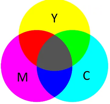
CYMK
The CYMK (cyan, yellow, magenta, key/black) is a subtractive colour model, mainly used in the printing industry. It is widely used in printing due to the ease with which it can be applied when utilising dyes of these colours on a white substrate. The principle of the method is that the white background is obstructed by varying combinations of the dyes used. Combining any two primary dyes results in the secondary colours of red, green and blue, as seen in Figure 2.15. The combination of all three results in a limited black, and so a black (Key) component is also required to reduce luminance when necessary.
36
Figure 2.15: Cyan, Magenta, and Yellow colour components, overlapping to
demonstrate the formation of secondary colours in the form of Red, Green and Blue.
The central region of imperfect black indicates the need for a Key/Black component in
[image:48.595.186.368.64.235.2]CYMK.
Figure 2.15 reveals a the cyan, magenta and yellow “primaries” of the CYMK model.
In this subtractive colour model, cyan is responsible for the absorption of long wavelengths (red), yellow absorbs blue, and magenta absorbs green. In this way, the gamut of CYMK can be constructed to form colour on a white background material. The variation of colour in printing is achieved by the varied distribution of different sized (often microscopic) ink patches on a white background material. In this model, chromaticity is indicated by the relative intensity of the CYM components, with luminance defined by that of Key/Black. In an 8-bit CYMK image, a vibrant red colour is achieved with a value of 0:255:255:0. To decrease the luminance of this red, the key/black component is increased, with a dark red achieved with a value of 0:255:255:255. Though this method has been widely used in colour printing technology, the requirement of a white substrate or equivalent surround material is a limiting factor in device design.
2.5.2
RGB
37 each colour significantly overlapping with the wavelengths ranges of the three colour cones in the retina. Similar to the CYMK model, RGB values combine both luminance and chromaticity of a colour, with luminance represented by the magnitude of each component, and the chromaticity determined by the combination all values. Instead of each component being responsible for the absorption of a region of the visible spectrum, they are instead directly correlated each colour cone. The secondary colours generated by mixing two RGB components are that of Cyan, Magenta, and Yellow, corresponding to the CYMK values of the previously mentioned method. Mixing of all three components results in white light, as shown in Figure 2.16.
Figure 2.16: Red, Green and Blue colour components, overlapping to demonstrate the
formation of secondary colours in the form of Cyan, Magenta, and Yellow, mirroring
that of the CYMK colour space in Figure 2.15. The central region of white corresponds
to the simulation of all three colour cones.
38
This model presents the best method for colour mapping of the structures considered in this thesis, as there is no requirement for a white background material, and there are less component colours needed to produce a full colour gamut. The key requirement of this model is that spectral features can be achieved in three broad, and easily defined regions of the visible region (red, green, and blue). These are more directly mapped to the values generated by the model, and require less interpretation than the CYMK model.
2.5.3
CIE
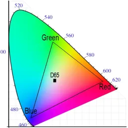
Colour clarity is a qualitative descriptor for the how a colour relates to the primary tristimulus values of red, green, and blue. The Commission Internationale de
L’Eclairage (CIE) 1931 colour-map is used to determine trends and qualitatively analyse colour clarity, and is presented in Figure 2.17. The CIE colour-map is often presented as an xyY plot, with each xy coordinate representing a chromaticity value. The third axis is denoted Y, expressing the luminance of the colour, and is often included as a value ranging from 0-100 at the data point, to maintain a 2-dimensional graph.
Figure 2.17: CIE colour-space map, indicating all chromaticity values at a luminance
value. Wavelengths around the border of the shoehorn indicate the chromaticity
[image:50.595.149.409.456.715.2]39 The centre point represents the area of lowest colour clarity, and indicates a spectrum that has equal stimulation of all three colour cone regions, in this case it is normalised to the D65 solar spectrum, a widely accepted standard for the RGB colour system[154,155]. This spectrum is presented later, in Figure 3.5.
Moving out from this centre point towards the border of the RGB region indicates an improvement in colour clarity, by increasing the saturation of the observed colour. As saturation is increased, the proportion of pure colour in the total sensation of observation[153] is increased. This means that the stimulation of a single colour cone is increasing, proportional to the other two, leading to more clear colours being observed. The red, green and blue tristimulus values represent the positions on the CIE colour-map that have the highest saturation in the RGB gamut, and so the highest colour clarity. In order for a colour to be positioned in close proximity to one of these positions, it must have a substantial reflectance intensity in only one of the three colour cone regions of the visible spectrum, while having significantly smaller reflectance in the other two. For example, an object with an observed colour near the blue primary with a large luminance has a high stimulation of the short (blue) colour cone receptors. This is due to a high reflectance intensity in the peak wavelength sensitivity range of 400-420 nm. The object also has a corresponding weak reflectance response at the middle (green) and long (red) wavelength ranges, and so appears a vibrant blue. This is similar for the positions near the red and green primaries, with stimulation of those particular wavelength ranges.
40
2.6
Conclusion
In this chapter, the main background concepts associated with the various stages of the thesis has been addressed. The spectral response of thin films has been examined, both in terms of interference and absorption, with applications in single and multilayer stacks.
Electron oscillations at metal-dielectric boundaries have been introduced, with a focus on LSPR. The importance of LSPR is paramount in nanostructures, as field enhancement at nanoparticle boundaries has a strong impact on the far-field reflectance, as well as scattering, and resonant absorption peaks.
The phenomenon of Fano resonance has been introduced, as they have a direct influence on two of the structures presented in Chapters 4 and 5.
41
Chapter 3
Methods
Summary
In this chapter, the methods employed throughout the thesis will be described in terms of their operation, and implementation later in the manuscript. The methods employed can be broken down into three main sections; Simulation, Fabrication, and Characterisation of the nanostructures under consideration.
The principle of the Transfer Matrix Method (TMM) is first described, as it is utilised in the simplest single, and multi-layer thin film structures. The TMM is capable of examining thin films comprised of materials with complex refractive indices, and is a fast simulation method over a wide wavelength range. Finite Difference Time Domain (FDTD) is introduced as a method for simulation of complex 3-dimensional structures. The commercial software Lumerical FDTD is used, with monitoring capability of the near, and far-field response of nanostructures. The description of a Python colour conversion script is also addressed, and is used wherever possible to determine colour response, and trends as geometries are varied.
Electron Beam Lithography (EBL), and other lithographic processes are introduced briefly, and the methods by which materials are deposited to form nanoscale structures are introduced.
42
3.1
Simulation
There are many configurations and parameters to consider when examining complex nanostructure architectures. Extensive simulation studies help to establish the structural parameters that are most sensitive to variation, and to achieve desired colours or switching capabilities of the structures. As fabrication is often costly and difficult at the nano-scale, these simulation studies are necessary in the development of a plasmonic nanostructure with the most optimal structure, that can then be fabricated. Due to the difficulty in fabrication of nanoscale devices, the results gained through simulation are important in saving time and narrowing the parameter space, and so must be robust and verifiable. In this thesis, several simulation techniques are used to determine the origin of the reflectance features, as well as the variation of certain spectral features as geometries are varied. Two primary simulation methods are used, Transfer Matrix for thin film structures, and Finite Difference Time Domain for more complex three-dimensional configurations.
3.1.1
Transfer Matrix Method
The Transfer Matrix Method (TMM) is a frequency domain numerical simulation technique that can be used to determine the transmittance, absorption, and reflectance spectra that result from a stack structure.
This method is based on a number of continuity conditions that occur with oscillating waves at the boundary of media with differing complex refractive
43
Figure 3.1: Diagram of beam with incident angle θ0, at a thin film interface, indicating
the boundary conditions for the electric field at a and b.
Figure 3.1 reveals the boundary conditions of the wave incident on a thin film at angle, θ0. It is important to note that this considers an incident wave with transverse
electric (TE) polarisation, where the electric field is perpendicular to the plain of incidence. From this, the E field at a and b interfaces can be determined as:
𝐸𝑎 = 𝐸0+ 𝐸𝑟1 = 𝐸𝑡1+ 𝐸𝑖1 (3.1a)
𝐸𝑏 = 𝐸𝑖2+ 𝐸𝑟2 = 𝐸𝑡2 (3.1b)
The relation of the E and B fields can be described by:
𝐵𝑎 = 𝛾0(𝐸0− 𝐸𝑟1) = 𝛾1(𝐸𝑡1+ 𝐸𝑖1) (3.2a)
𝐵𝑏= 𝛾1(𝐸𝑖2+ 𝐸𝑟2) = 𝛾𝑠𝐸𝑡2 (3.2b)
According to[156]:
𝐵 =𝑛
𝑐𝐸 = 𝑛√µ0𝜀0𝐸 (3.3)
where γ is:
𝛾0 = 𝑛0√µ0𝜀0cos 𝜃0 (3.4a)
44
𝛾𝑠 = 𝑛𝑠√µ0𝜀0cos 𝜃2 (3.4c)
The phase difference that develops due to travelling through the layer, is described by[156]:
𝜎 =2𝜋
𝜆0 𝑛1𝑑 cos 𝜃1 (3.5)
where λ0 is the wavelength of the incident light in layer n0. The formation of the
transfer matrix from this, is described in detail by Pedrotti[156], with the matrix (M) for each layer described as:
𝑀 = [ Cos (𝜎)
𝑖𝑆𝑖𝑛(𝜎) 𝛾
𝑖𝛾𝑆𝑖𝑛(𝜎) 𝐶𝑜𝑠(𝜎)
] (3.6a)
where
𝑀 = [mm11 m12
21 m22] (3.6b)
The matrix in Equation 3.6a is used to represent each layer, and by multiplication, determines the system matrix (MT) of the entire stack, as:
𝑀𝑇 = 𝑀1𝑀2𝑀3… 𝑀𝑁 (3.7)
Here, MN is the matrix for each layer in the stack of arbitrary layers. From this the
transmission (t) and reflection (r) coefficients can be determined by[156]:
𝑡 = 2𝛾0
𝛾0𝑚11 + 𝛾0𝛾𝑠𝑚12 + 𝑚21 + 𝛾𝑠𝑚22 (3.8a)
𝑟 = 𝛾0𝑚11 + 𝛾0𝛾𝑠𝑚12 − 𝑚21 − 𝛾𝑠𝑚22
𝛾0𝑚11 + 𝛾0𝛾𝑠𝑚12 + 𝑚21 + 𝛾𝑠𝑚22 (3.8b)
From these the Transmission (T) and Reflection (R) as a fraction of incident light intensity can be determined by:
𝑇 = |𝑡|2 and 𝑅 = |𝑟|2 (3.9)
Absorption can be measured as:
45 For a TE polarised incident wave the γ1 value is determined by Equation 3.4b
However, in transverse magnetic (TM) polarisation, the γ1 value is determined by:
𝛾1 = 𝑛1√µ0𝜀0
cos 𝜃1 (3.11)
For unpolarised light at an angular incidence, an average of the reflectance can be taken, such that:
𝑅 =1
2(𝑅𝑇𝐸 + 𝑅𝑇𝑀) (3.12)
All simulations in this thesis are carried out at normal incidence, with light incident perpendicular to the surface of the layer, and so the γ1 values are the same for TE
and TM polarisations.
This simulation method is suitable for thin film reflectance, transmission and absorption in single, or multi-layer stacks of materials. The technique is validated against literature in Chapter 6, used extensively in the thin film VO2 study carried out in that Chapter.
3.1.2
Finite Difference Time Domain
Finite Difference Time Domain (FDTD) can be used to simulate the electrodynamics of more complicated, three-dimensional nanoscale structures comprised of non-magnetic materials. Lumerical FDTD is a widely used commercial tool, in which simulations are generated in a Computer Aided Design (CAD) style visualisation tool that examines a simulation volume. This simulation volume is comprised of geometric components, where each object has the frequency-dependent complex refractive index information contained. A three-dimensional mesh permeates throughout the entire structure, in which the mesh intersections are the positions at which the electric and magnetic field are measured. This technique utilises the partial differential form of the time-dependent Maxwell’s equations, and solves the