Published by Science and Education Publishing DOI:10.12691/amp-7-1-1
Preparation and Characterization of Vanadium
Pentoxide by DC-Magnetron Sputtering
Mohammed. K. Kalaf1, Sabri. J. Mohammed2, Mohammed. Sh. Muhammed3,*
1
Ministry of Sciences and Technology, Baghdad, Republic of Iraq 2
Tikrit University, Physics Department, Tikrit, Republic of Iraq 3
Education Mission, Education Department, Salah al-Din, Iraq *Corresponding author: [email protected]
Received February 18, 2019; Revised April 11, 2019; Accepted April 19, 2019
Abstract
In this work, the structural properties of the monocrystalline vanadium pentoxide have been presented. Vanadium pentoxide (V2O5) films were deposited by using a DC reactive magnetron sputtering system at a working pressure of 8.5x10⁻²mbar.The sputtered vanadium atoms were sputtered and oxidized in presence O2:Ar gas mixture by (5/95,10/90, 20/80,30/70,50/50). Employment of magnetron results in the formation of V2O5 in the final samples according to the XRD analysis, increase the roughness and hence surface area of the produced V2O5 nanostructures. The results of X-rays are shown to us, the deposited films were formed by nanoparticles with an average grain size in the range of (52.11nm to 98.03) nm and roughness Ave (nm) in the range of (1.04nm to 8.88nm). The deposited films are identified to be polycrystalline nature with a cubic structure along ((001), (111)) and ((200)) orientation also MonoV2O5, Cub VOwere found as deposited. The texture of the films was observed using SEM and AFM, it was observed that the grain size was increased with increasing the O2 percentage. These improvements in the structural properties of the produced vanadium pentoxide make these nanostructures good candidates for specific applications, such as photo detectors, solar cells, electro chromic smart window and gas sensor.Keywords
: magnetron sputtering, vanadium, structural propertiesCite This Article:
Mohammed. K. Kalaf, Sabri. J. Mohammed, and Mohammed. Sh. Muhammed, “Preparation and Characterization of Vanadium Pentoxide by DC-Magnetron Sputtering.” Applied Mathematics and Physics, vol. 7, no. 1 (2019): 1-7. doi: 10.12691/amp-7-1-1.1. Introduction
Vanadium creates a wide range of composites with oxygen which have variation structural and different valence states and founds in a many phases of oxide comprise of vanadium oxide, There are at least 15 variation vanadium oxides communally to now, for example; VO, V2O3, VO2, V2O5, V6O13 and so on [1]. V2O5 are known to be the most stable compound form for vanadium metal , but other non-stable stoichiometry can be constrained under particular oxidation conditions. Different phases of vanadium oxides can be obtained by controlling the deposition method parameters, or by proportion process manipulate, e.g., additional thermal annealing .properties of these phases of vanadium oxides depend on their structure, which determines other properties which exhibit a complex stoichiometric composition [2]. Thin-walled oxide nanoparticles belong to this smart inventory list, and these thin-layer oxide structures have been accelerated for practical applications such as electronics and optoelectronics. Most of these vanadium oxides are characters for the transfer of semiconductor phases to metal to reversible [3], which is accompanied by large changes in infrared optical
0, +2, +3, +4 and +5, respectively, are related to phases V, VO, V2O3, VO2 and V2O5. Two sets of compost properties are identified as stable phases. These series VnO2n-1 and VnO2n + 1 are defined as magnetism [11,12]. Wesley phases, respectively, and they connect the three most common phases, V2O3, VO2 and V2O5 [11,13,14]. The working mechanism of electro chromic materials consists of electrolyte, intercalated mobile ions which performs intercalation/de intercalation while a potential difference is applied. For this purpose, layered structure of V2O5 is a promising material. The most commonly used phases, which found in wide range of applications due to their novel properties, are the VO, VO2, V2O3, and V2O5 oxide phases [15].
2. Experimental Details
Vanadium pure was chosen as the primary material to study for this project. Sputtering processes normally uses argon gas because it does not react with the target material allowing thin films to be formed. The addition of a gas that reacts with the target material, such as oxygen, will form compounds of the material and the reactant. To determine how vanadium oxide is formed using reactive magnetron sputtering a reactive gas test was performed. Because the sputtering system uses a DC power supply that allows both voltage and current to float while maintaining constant power, the target voltage can be easily measured and used to infer changes in the impedance of the sputtering plasma. The gun in which the target is mounted is designed to provide a narrow range of impedance to the power supply. With the addition of a reactive gas the impedance of the target changes. Using the fixed conditions of 660V of DC power and a chamber pressure of 0.08 mb while introducing increased amounts of oxygen the voltages were recorded.
Figure 1. The main experimental setup used in this work
3. Results and Discussion:
Figure 2 shows the XRD patterns for the VOX nanoparticles coating layer deposited at various Ar/O2
ratio, ranging from 5% to 50 %. For a deposition time of 120 min and a sputtering power of 680V, within the range of Ar pressure, the thickness of the VOX films ranges from 59.6 to 212 nm. The intensity of the (001) peak for the V2O5 nanoparticles coating layer deposited at lower Ar/O2 ratio was observed to be higher compared with those deposited at higher Ar/O2 ratio. The intensity of a peak in the X-ray diffraction pattern is a direct measure of the film crystallinity. We attribute this phenomenon to the increase of the surface mobility of the adatoms with higher energy and decreasing Ar/O2 pressure, which is necessary to form a highly crystalline film. In this respect, high Ar/O2 -pressure in the sputtering process infers the decrease in the surface mobility of the adatoms after series of particle collisional events during the travel from the deposition source to the substrate [16]. In other words, at low pressure the electron temperature is high. at high temperature, more energy should be available for the atoms to acquire so that they may diffuse and occupy the correct site in the crystal lattice. This result is consistent with previous study [16].
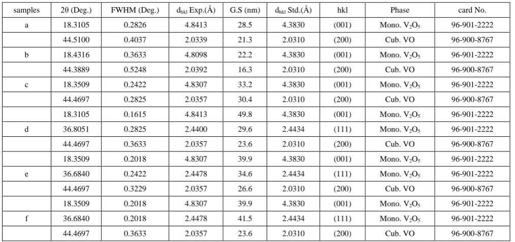
The VOX films exhibit peaks corresponding to the mono V2O5 phase at 2θ = 18.3105°, 18.3105°,18.3509°, 36.8051° and 36.6840° direction identify with standard peaks[ card. No (96-901-2222) and also the XRD pattern illustrates that the vox films had a polycrystalline structure with peaks attributed to Cub VO phase at 2θ =44.5100° and 44.4697° direction identify with standard peaks [card. No(96-900-8767). The XRD pattern illustrates that the (V2O5) films have polycrystalline (111), (001) and The X-ray diffractions of the Vanadium target is also displayed cub (VO). All the XRD patterns show same behavior where the FWHM decreases with increase of the different Ar:O2 ratio with increasing the crystallite size [17,18].
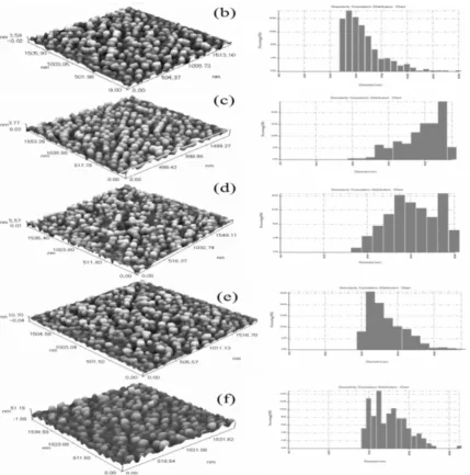
3.1. Atomic Force Microscope (AFM)
Figure 3 shows the two-dimensional (2D) and three- dimensional (3D) AFM images of (VOx) deposited at different gas (Ar/O2) mixture ratio on the glass substrate. The 2D images show that the films are uniform and the substrate surface is well covered with grains that are nearly uniformly distributed over the surface. the surface morphology reveals the Nano-crystalline (VOx) grains. The 3D images reveal that there is a large sharp island or particles formation observed in deposited films microstructure. From the images, it was observed that the surfaces of the films exhibited a certain degree of roughness. The surface roughness gives further information about surface morphology of thin films. The variation in surface roughness of thin film plays an important role in optical coatings. It improves the optical absorbance and influences the optical properties of thin films. In addition, Surface roughness is directly proportional to the gas sensitivity of the film since larger roughness results in a larger contact area with gaseous species [19]. The average grain size and root mean square roughness (RMS) of these films are shown in the Table 2.
samples displayed are granular structure. The granular films show a higher surface area, which is conducive for film-gas interaction and results in higher gas sensitivity [20]. The gas sensitivity has a proportional relationship with film roughness [21]. All the images appeared in figure (4.17) show homogeneous cluster distribution with columnar structure; where the average grain size values
decrease slightly with increasing oxygen flow. Increasing oxygen flow leads to increase in the number of oxygen molecules adsorbs on the substrate surface which acts as traps for atoms causing to reduce grain size for thin films by increasing the number of nucleation centers, Also, increases roughness with increasing oxygen flow which leads to increase the vertical growth on the substrate surface.
Figure 2. X-ray diffraction patterns for a thin sheet of vanadium deposited with different ratios of Ar:O2
Table 1. X-ray diffraction patterns for a thin sheet of vanadium covered with different ratios of Ar: O2
samples 2θ (Deg.) FWHM (Deg.) dhkl Exp.(Å) G.S (nm) dhkl Std.(Å) hkl Phase card No.
a 18.3105 0.2826 4.8413 28.5 4.3830 (001) Mono. V2O5 96-901-2222
44.5100 0.4037 2.0339 21.3 2.0310 (200) Cub. VO 96-900-8767
b 18.4316 0.3633 4.8098 22.2 4.3830 (001) Mono. V2O5 96-901-2222
44.3889 0.5248 2.0392 16.3 2.0310 (200) Cub. VO 96-900-8767
c 18.3509 0.2422 4.8307 33.2 4.3830 (001) Mono. V2O5 96-901-2222
44.4697 0.2825 2.0357 30.4 2.0310 (200) Cub. VO 96-900-8767
18.3105 0.1615 4.8413 49.8 4.3830 (001) Mono. V2O5 96-901-2222
d 36.8051 0.2825 2.4400 29.6 2.4434 (111) Mono. V2O5 96-901-2222
44.4697 0.3633 2.0357 23.6 2.0310 (200) Cub. VO 96-900-8767
18.3509 0.2018 4.8307 39.9 4.3830 (001) Mono. V2O5 96-901-2222
e 36.6840 0.2422 2.4478 34.6 2.4434 (111) Mono. V2O5 96-901-2222
44.4697 0.3229 2.0357 26.6 2.0310 (200) Cub. VO 96-900-8767
18.3509 0.2018 4.8307 39.9 4.3830 (001) Mono. V2O5 96-901-2222
f 36.6840 0.2018 2.4478 41.5 2.4434 (111) Mono. V2O5 96-901-2222
Figure 3. Three-dimensional (3D) AFM images of vanadium oxide thin films deposited on glass substrate with Granularity and the height distribution Analysis image at different ratios of Ar: O2
Table 2. 3D AFM image and their granularity accumulation distribution for thin films at different Ar:O2 ratio
O2:Ar ratio Average
Diameter (nm)
RMS roughness (nm)
Roughness Ave.(nm)
(5/95)% 52.11 0.881 1.04
(10/90)% 63.57 0.902 1.04
(20/80)% 58.52 1.31 1.53
(30/70)% 51.47 2.42 2.85
(50/50)% 98.03 7.37 8.88
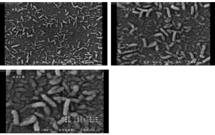
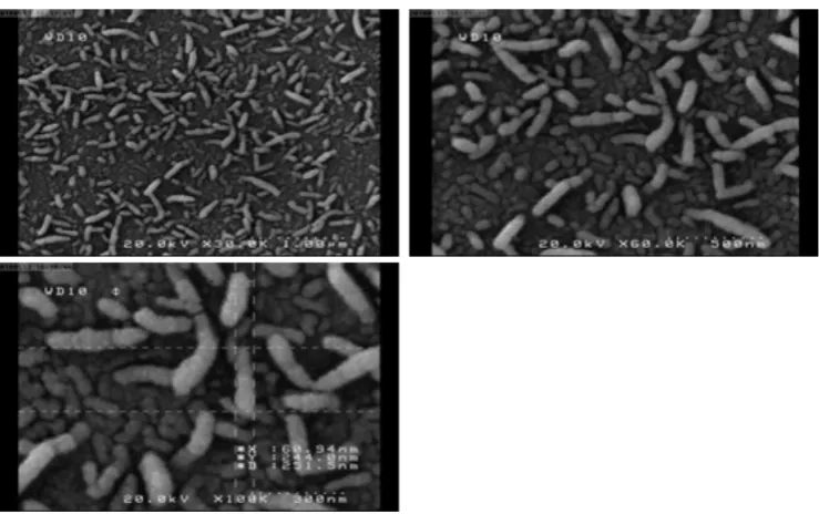
3.2. Scanning Electron Microscope (FESEM)
Figure 4 - Figure 8 show the surface morphology images of VOX thin film with different gas(Ar/O2) mixture ratio. We can see clearly demonstrated particles having the uniform, homogenous distribution. FESEM micrograph shows that the deposited coating layer consists of VOX nanoparticles with very small diameters at different gas (Ar/O2) mixture and constant working pressure. It shows that the sputtered particles diameter are increased, from 36.9 nm to 251.5 nm. This may be due to
Figure 4. Field emission scanning electron microscopy (FE-SEM) images for Vanadium oxide with gas rate mixture (Ar/O2)=(95/5)
Figure 5. Field emission scanning electron microscopy (FE-SEM) images for Vanadium oxide with gas rate mixture (Ar/O2)=(90/10)
Figure 7. Field emission scanning electron microscopy (FE-SEM) images for Vanadium oxide with gas rate mixture (Ar/O2)=(70/30)
Figure 8. Field emission scanning electron microscopy (FE-SEM) images for Vanadium oxide with gas rate mixture (Ar/O2)=(50/50)
4. Conclusion
FE-SEM investigations showed that the nanoparticles obtained at gas rate mixture (50%) more larger in size than obtained at gas rate mixture (5%) and the particle size increase with increasing gas mixture ratio. An analysis of the structural properties of vanadium powder oxide produced by reactive spectrometry has been observed. An increase in the surface roughness of the samples was observed with an increase in the ratio of the mixture of gases. This allows for the use of samples prepared in the use of gas sensors. The FE-SEM images showed that the particles size increase from 36.9 to 251.5 nm when the gas mixture rate increased from 5% to 50%. The X-ray diffraction studies have confirmed that VOX sample has the Mono (V2O5) phase while remaining samples have a cubic(VO) phase. The intensity of the major peaks was decreased and shifted toward higher 2θ angles when Oxygen ions increase.
Acknowledgements
The search is performed as part of the execution PhD "program of the Ministry of Higher Education Education//2019/01/1. "Developing methodology Nanoparticles for thin films.
References
[1] Schneider K, 2015. Structural and optical properties of VOx thin films. Archives of Metallurgy and Materials. 60.2 957-961 [2] Golan G et al, 2004. Investigation of phase transition mechanism
in vanadium oxide thin films. Journal of Optoelectronics and Advanced Materials. 6.1 189-195.
[3] Warwick, M. E, & Binions, R, 2014. Advances in thermochromic vanadium dioxide films. Journal of Materials Chemistry. A 2.10 3275-3292.
[5] Liu Yueyan et al, 2016. Effect of annealing temperature on the structure and properties of vanadium oxide films. Optical Materials Express. 6.5 1552-1560.
[6] Zou Mengyang, 2015. Deposition Methods and Thermoresistive Properties of Vanadium Oxide and Amorphous Silicon Thin Films PhD Thesis. University of Dayton.
[7] M Farahmandjou, 2017. Chemical Synthesis of Vanadium Oxide (V2O5) Nanoparticles Prepared by Sodium Metavanadate. J. Nanomedicine Res. 5.1 2-5.
[8] Lamsal Chiranjivi Ravindran M, 2013. Optical properties of vanadium oxides-an analysis. Journal of materials science. 48.18 6341-6351.
[9] Urena Begara, Ferran Crunteanu, Aurelian Raskin, Jean-Pierre, 2017. Raman and XPS characterization of vanadium oxide thin films with temperature. Applied Surface Science. 403 717-727 . [10] Vijayakumar Yelsani et al, 2015. Influence of the substrate
temperature on the structural, optical and thermoelectric properties of sprayed V2O5 thin films. Material in technologies .49.2 17 .
[11] Ramplberg Geert et al, 2015. In situ X-ray diffraction study of the controlled oxidation and reduction in the V–O system for the synthesis of VO2 and V2O3 thin films. Journal of Materials
Chemistry .C3 43 11357-11365 .
[12] Jeong Jaewoo et al, 2013. Suppression of metal-insulator transition in VO2 by electric field–induced oxygen vacancy formation Science. 339. 6126. 1402-1405.
[13] Masina, Bathusile N et al, 2015. Optimizing the synthesis of vanadium–oxygen nanostructures by plasma plume dynamics using optical imaging. Optical Engineering .54.3 037106.
[14] Fay Alexander, 2005. Engineering in vernetzten, offenen, durchgängigen Systemen (Engineering in Linked and Open Systems). at-Automatisierungstechnik. 53.4-5 205-210.
[15] Yimam, E, 2015. Fabrication of Vanadium Oxide Nanoparticles by Pulsed Laser Ablation.
[16] Chan, K. Y., & Teo, B. S, 2007. Effect of Ar pressure on grain size of magnetron sputter-deposited Cu thin films. IET Science,
Measurement & Technology. 1(2) 87-90.
[17] Koduru et al G, 2013. Spectroscopic and electrochromic properties of activated reactive evaporated nano-crystalline V 2 O 5 thin films grown on flexible substrates. International Nano Letters. 3(1) 24.
[18] Cui, et al, 2008. Thermochromic properties of vanadium oxide films prepared by dc reactive magnetron sputtering. Thin Solid Films. 516(7), 1484-1488.
[19] Prajapati, C. S., & Sahay, P. P, 2013. Influence of In doping on the structural, optical and acetone sensing properties of ZnO nanoparticulate thin films. Materials Science in Semiconductor Processing .16(1) 200-210.
[20] S. C. Gadkari, et al, 2005 Solid state sensors for toxic gases", Technical physics and prototype Engineering Division Bhabha Atomic Research Centre. 49.
[21] N. G. Deshpandea, et al, 2009. Studies on tin oxide-intercalated polyaniline nanocomposite for ammonia gas sensing applications", Sensor and Actuators B. 138 76-84.
[22] Cerqueira et al, 1995. Microcrystalline silicon thin films prepared by RF reactive magnetron sputter deposition. Vacuum. 46(12) 1385-1390.
[23] Nag, J., Haglund, R., & Payzant, A, 2011. Effects of growth temperature on epitaxial thin films of vanadium dioxide grown by pulsed laser deposition. In CLEO: Applications and Technology Optical Society of America.p. AMA5
[24] Berezina, et al, 2015. Vanadium oxide thin films and fibers obtained by acetylacetonate sol-gel method. Thin Solid Films. 574 15-19 .
[25] Luo et al, 2014. Effects of thickness on the nanocrystalline structure and semiconductor-metal transition characteristics of vanadium dioxide thin films. Thin Solid Films. 550, 227-232.
[26] Chen et al, 2017 Effects of annealing on thermochromic properties of W-doped vanadium dioxide thin films deposited by electron beam evaporation. Thin Solid Films. 644, 52-56.