FAST AND OPTIMAL DESIGN OF A K-BAND TRANSMIT-RECEIVE ACTIVE ANTENNA ARRAY
S. Yang, Q. Liu, J. Yuan, and S. Zhou
National Key Laboratory of Antennas and Microwave Technology Xidian University
Xi’an 710071,China
Abstract—An active-antenna array with 18 transmit elements and 18 receive elements is designed and fabricated. This T/R array can work at two different frequencies (19.5 GHz and 21.5 GHz) with multiple
levels of isolation between the transmit and receive channels. A
hybrid element-level vector finite element and adaptive multilevel fast multipole method (ELVFEM/AMLFMA) is applied to simulation the performance parameters of the array element and the full array fast. To obtained the maximum directivity of the array,the best distances of the T/R elements in the array are optimized by using the genetic algorithm (GE) combining with VFEM/AMLFMA. The design efficiency of the array is improved at a ratio of 30%. Finally the performance of the T/R array fabricated is measured in experiments and some good results are obtained.
1. INTRODUCTION
Active-antenna array technology combines printed antennas and active devices with the goal of improving performance,increasing functional-ity,and reducing size relative to alternative architectures. Such arrays show potential for use in millimeter-wave commercial applications such as wireless local-area networks,electronic identification systems,and vehicle collision-avoidance radar.
The fundamental goal of the work of this paper is to achieve full-duplex operation by using two different frequencies (19.5 GHz and 21.5 GHz) with multiple levels of isolation between the transmit
and receive channels. The primary application for this full-duplex
signals are received from free space,amplified,and focused onto a receiver at the focal point.
2. SIMULATION METHOD
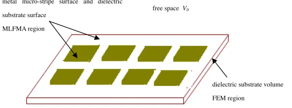
To analysis plane micro-stripe antenna array like shown in Figure 1,hybrid finite element and multilevel fast multipole method (FEM/MLFMA) can be applied. The field in the region of dielectric substrate can be formulated into an equivalent problem with the function
F(E) = 1 2
V
1
µr
(∇ ×E)·(∇ ×E)−k20εrE·E
dV
+jk0
Se
(E×H)·ndSˆ (1)
where
V interior volume of the substrate;
Se outside surface of the antenna; ˆ
noutward unit normal to antenna surface;
k0 free-space wave number;
On the antenna surface Se,a group of combined field integral equation (CFIE) can be employed for both the micro-stripe and substrate surface.
α·EFIE + (1−α)·MFIE (0.2≤α ≤1) (2)
In Equation (2),EFIE is the electric field integral equation and MFIE is the magnetic field integral equation. Let’s assume that the antenna
metal micro-stripe surface and dielectric substrate surface
MLFMA region
dielectric substrate volume FEM region
free space V0
is combined ofM−1 metal parts and a dielectric substrate part,and the region they occupied is Vl(l= 1. . . M). The region V0 out of the
antenna is defined as free space. M+ 1 equations should be needed for the problem we discussed.
On the boundary ofV0 region EFIE yields
Es(r) =−jk0η
S0
J0(r)G(r,r)dr− ∇ ×
S0
M0(r)G(r,r)dr
(3)
MFIE yields
Hs(r) =−jk0 η
S0
M0(r)G(r,r)dr+∇ ×
S0
J0(r)G(r,r)dr
(4)
where J = ˆn×H and M = E ×nˆ, J denotes the electric current on boundary surface and M denotes magnetic current on boundary surface. G(r,r) and G(r,r) are the Green’s function and dyadic Green’s function in free space.
On the boundary ofVi region,EFIE yields
0 = −jkη
Sl
Jl(r)G(r,r)dr− ∇ ×
Sl
Ml(r)G(r,r)dr (5)
(M = 0 for the metal surface)
MFIE yields
0 =−jk η
Sl
Ml(r)G(r,r)dr+∇ ×
Sl
Jl(r)G(r,r)dr (6)
Combing Equations (1),(3)–(6) and using vector edge basis function,we can obtain the matrix equation of complete system
KII KIS 0
KSI KSS B
0 P1 Q1
· · ·
0 PM QM
0 P0 Q0
EI ES H1S
·
HM S H0S
= 0 0 b1 ·
bM S b0 (7)
[KII],[KIS],[KSI],[KSS],and [B] are sparse submatrices and,in particular,[KII] and [KSS] are symmetric,[B] is skew symmetric and [KIS] = [KSI]T,where the superscript T denotes a transpose operation. [P] and [Q] are the dense submatrices of discretized CFIE which is employed onSe.
To improve the performance of FEM,the multiply of [K] and vector can be change into the multiply of a series of small scale matrices and vector. The [K] yields
K =
N
i=1
Ki (8)
where [Ki] is the global coefficient matrix of ith volume tetrahedral element in [K] and N is the total number of tetrahedral elements. In matrix [Ki] the matrix elements on the rows and columns related to
ith volume tetrahedral element of regionV are not equal to zero,these elements are also the elements in the coefficient matrix of ith volume tetrahedral element. Thus,the multiply of [K] and unknown vector yields
b=Kx=
i Kix
=
i
(Kix) = i
(Kixi) = i
bi (9)
where
b={0,0,b}T, x={EI,ES,Es}T
In Equation (9), {xi} is the vector corresponding to [Ki],the nonzero elements in {xi} are the elements in {x}. The multiply of [Ki] and {xi} is determined by ith volume tetrahedral element only and [Ki]{xi}= [Ki]{xi},where [Ki] is the small scale dense coefficient matrix ofith volume tetrahedral element and{xi}is the corresponding unknown vector of [Ki]. The multiply of global coefficient matrix [K] and unknown vector {EI,ES,HS}T can be calculated at element-level. Because the multiply calculation of zero elements in [Ki] and corresponding elements in{xi}can be omitted and all the computation is finished at element-level,the CPU time and memory requirement of FEM can be reduced significantly and this method can be called as element-level vector finite element method(ELVFEM).
In Equation (7),each linear matrix equation ofVl surface can be written as
Ns
i=1
Pjiesi+ Ns
i=1
when MLFMA is applied. Where
Ns
i=1
Pjiesi =
i /∈Gm
Pjiesi+
s
d2kVPf mj
k
·
m∈Gm TL
k·rmm i∈Gm
Vsmi k esi (11) Ns i=1
Qjihsi =
i /∈Gm
Qjihsi+
s
d2kVQf mj
k
·
m∈Gm TL
k·rmm i∈Gm
Vsmi
k
hsi (12)
esi∈ {ES}, hsi ∈ {HS}
Ns is the number of surface triangle elements, Vsmi, TL and Vf mj are aggregation operator,translation operator and disaggregation operator. While using the advanced MLFMA method called adaptive multilevel fast multipole algorithm (AMLFMA) [1],formulation (11) and (12) can be written as
Ns
i=1 ZjiIi=
i /∈Gm
ZjiIi+
s
d2kVSP Df mj
k
·
m∈Gm F F T−1
F F T
TL
k·rmm
×F F T
i∈Gm
V∗smSP Di k Ii
+VSP Df mj
k0
·
m∈SF Gm F F T−1
F F T
TLf ar
×F F T
i∈SF Gm
V∗smSP Di k0 Ii (13)
In AMLFMA the fast Fourier transformation (FFT) is used to calculate the translation process of MLFMA and higher performance can be obtained.
3. ANTENNA DESIGN 3.1. Element Design
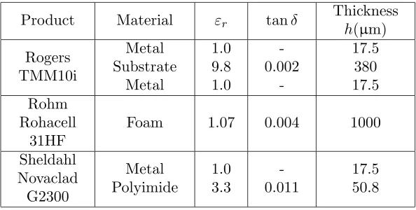
The T/R array is comprised of three layers of dielectric [2,18]. The primary layer is Rogers TMM10i,the middle layer is Rohm Rohacell 31 HF,and the last layer is Sheldahl Novaclad G2300. The substrate which supports the majority of the microwave circuitry is Rogers TMM10i with a thickness of 381µm,a relative permittivity of εr = 9.806,a loss tangent of tanδ = 0.002,and a metal thickness of 17.5µm. To prevent loss in the form of surface waves,the substrate was chosen to be thin (λd= 13) relative to the dielectric wavelength [2]. Substrate values are summarized in Table 1.
Table 1. Array substrate parameters shown in order of assembly.
Product Material εr tanδ
Thickness
h(µm)
Rogers TMM10i
Metal Substrate
Metal
1.0 9.8 1.0
-0.002
-17.5 380 17.5 Rohm
Rohacell 31HF
Foam 1.07 0.004 1000
Sheldahl Novaclad G2300
Metal Polyimide
1.0 3.3
-0.011
17.5 50.8
Standard and slot-fed patches are the fundamental building blocks of the array. The slot-fed patch simultaneously increases aperture efficiency and provides a coupling path through the array. The standard patch on the high permittivity substrate is small enough to be integrated into the complex front side circuitry while still providing reduced coupling relative to other antennas.
The MSL provides connectivity to the standard patch antennas and slot couplers,and the CPW provides transitions to and from the MMIC. The benefit of using a hybrid CPW-MSL design as opposed to a simpler all-MSL design is the reduction of fabrication complexity by the elimination. The final dimensions for the transmission lines are summarized in Table 2.
Table 2. Transmission-line specifications.
CPW Dimensions MSL Dimensions Substrate Values
Wcpw 290µm Wms 360µm εr 9.8
Scpw 245µm λms 6.0 mm tanδ 0.002
Bcpw 780µm h 380
λcpw 6.5µm t 17.5
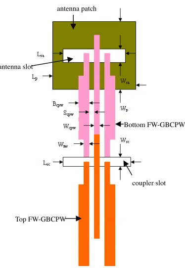
Probe-station measurements require that the input and output port (even in the case of a radiator) are on the same side of the substrate and that probed ports terminate in a CPW transmission line. This necessitates the use of multiple transitions to measure the various unit-cell components. The design of novel testing circuitry,as well as unit-cell components used in the final implementation of the array are presented in Figure 2.
Table 3. Dimensions of the slot coupler and antennas.
Coupler Dimensions Slot Dimensions Slot-Fed Patch Dimensions
Lsc 3.55 mm Lsa 4.65 mm Lp 6.55 mm Wsc 0.35 mm Wsa 1.20 mm Wp 5.90 mm
The slot coupler is comprised of two CPW-to-MSL transitions aligned on opposite sides of a slot in a shared substrate ground plane. The transition from CPW to MSL occurs in three coupled micro-stripe transmission lines.
antenna slot
coupler slot
Top FW-GBCPW
Bottom FW-GBCPW antenna patch
Figure 2. Balanced coupler and patch antenna with characteristic geometric parameters labeled. K-band ground-backed CPW balanced coupler with the transition-fed patch antenna.
3.2. Element and Channel Coupling
Amplification is performed in transmission (19.5 GHz) by an HPHMMC-5620 single-bias power amplifier (PA) with a maximum small-signal gain of 17 dB from 6 to 20 GHz (Figure 3(a)). Amplification is performed in reception (21.5 GHz) by an Alpha AA022N1-00 single-bias low noise amplifier (LNA) with a maximum small-signal gain of 22 dB from 20 to 24 GHz and a noise figure of 2.5 dB (Figure 3(b)).
The reduction of the coupling from input to output antenna is achieved by the use of orthogonal polarizations for the input and output antennas,and by a ground plane,which separates the input and output antennas. Thus,the only antennas which are copolarized are antennas of the other channel on the opposite side of the ground plane.
(a) (b)
Figure 3. Power amplifier (a) and low-noise amplifier (b) specifications. The power amplifier amplifies the outgoing 19.5 GHz channel. The low-noise amplifier amplifies the incoming 21.5 GHz channel.
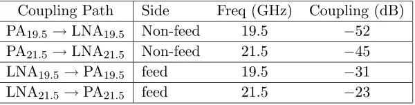
Table 4. Simulated coupling between channels in the passive array.
Coupling Path Side Freq (GHz) Coupling (dB) PA19.5 →LNA19.5 Non-feed 19.5 −52
PA21.5 →LNA21.5 Non-feed 21.5 −45
LNA19.5→PA19.5 feed 19.5 −31
LNA21.5→PA21.5 feed 21.5 −23
3.3. Unit-cell Design
A single full-duplex transmit-receive unit cell is comprised of two independent orthogonal unit cells,one for each channel (Figure 4 and Figure 5). A single channel’s unit cell contains a patch antenna, a coplanar waveguide section with amplifier,and a slot-fed patch antenna. A unit cell dimension measures 8.0×16.0 mm2.
transm it unit-cell(19.5GHz)
receive unit-cell(21.5GHz) PA
LNA FWCPW
standard patch
bias line MSL to CPW transition
Slot fed patch
capacitor
Figure 4. The 19.5 GHz transmit (left) and 21.5 GHz receive (right) unit cells with important features labeled.
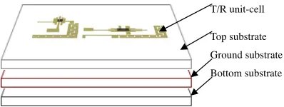
Top substrate
Ground substrate
Bottom substrate T/R unit-cell
Figure 5. Assembly drawing of the transmit and receive unit cells.
coplanar waveguide (fCPW) within a single unit cell. The MSL provides the connection to the standard patch antenna on the feed side of the array; the fCPW provides a transition to the MMIC, which eliminates the need for vias required with MSL. Transitions between MSL and fCPW occurs in a section of three coupled micro-stripe transmission lines of lengthλms/4 at the unit-cell’s frequency of operation.
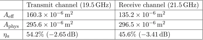
The aperture efficiencies of the unit cells are summarized by using ELVFEM/AMLFMA in Table 5. The aperture efficiencies are calculated with Equation (14) using the area of two unit cells asAphys.
It should be noted that the aperture efficiency of the array is most strongly influenced by the array’s overall array factor rather than by the individual unit cell,but is included here to highlight the relative directivities of the antennas.
Aperture efficiency is the ratio of the effective area of a spatial power combiner to the physical area.
ηα =
Aeff Aphys
(14)
The effective area of a spatial power combiner is proportional to the directive gain
Aeff = λ2
4πG (15)
which is related to directivity by
G=ηrD (16)
whereηris the system efficiency which includes substrate losses,ohmic losses,and polarization and impedance mismatches.
Table 5. Antenna aperture-efficiency calculations.
Transmit channel (19.5 GHz) Receive channel (21.5 GHz)
Aeff 160.3×10⁻⁶m2 135.2×10⁻⁶m2 Aphys 295.6×10⁻⁶m2 296.5×10⁻⁶m2
ηa 54.2% (−2.65 dB) 45.6% (−3.41 dB)
Because the slot-coupler transition is used to feed the slot-fed patch antenna,it is the first circuit characterized. The simulated return loss by using ELVFEM/AMLFMA of the coupler is less than 10 dB over a 12% bandwidth from 17 GHz to 20 GHz with a 2 dB average insertion loss over the pass band (Figure 6).
3.4. Array Layout Design and Optimization [4–12, 14, 20, 21]
distances of elements in the array,genetic algorithm is used to optimize the array layout to obtained both the maximum directivity of transmit array and receive array [5–7].
16 18 20 22 24 -20
-15 -10 -5 0
S21(dB
)
Frequency(GHz)
s imulat ed
16 18 20 22 24 -18
-16 -14 -12 -10 -8 -6 -4 -2 0
S11(dB)
Frequency(GHz) s imulat ed
(a) (b)
Figure 6. Simulated reflection (a) and transmission (b) coefficients of the slot coupler.
Figure 7. The CAD model of K-band full-duplex transmit-receive active-antenna array shown from the feed side.
Defined the directivity of a planner array includeN×N elements as
D= 2π 4π
0
π
0 |F(θ, φ)|
where
F(θ, φ) = 4 cosθ
N
x
m=1
Ixmcos
k
m
i=1 dxi−
1 2dx1
sinθcosφ
× Ny n=1 Iyncos
k
n
j=1 dyj−
1 2dy1
sinθsinφ
(18)
to obtained the best directivity,the current Imn(Imn = IxmIyn), distancesdxi and dyj inxdirection and y direction should be selected as the variables to be optimized.
For the array include both T/R channels,the target function and the fitness function can be selected as
f = max (α1DT +α2DR) = min
−α12π 4π 0
π
0 |FT(θ, φ)|
2sinθdθdφ −α2
4π
2π
0
π
0 |FR(θ, φ)|
2sinθdθdφ
(19)
(0< α1 <1, 0< α2<1, α1+α2 = 1)
fitness =α1DT +α2DR (20) whereDT andDRare the directivities of the transmit array and receive array, a1 and a2 are the weight coefficients. The currents and the
distances in the two directions of both the transmit array and receive array are the variables to be optimized.
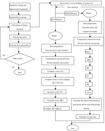
cluster. The optimization efficiency is improved at a ratio about 30%. The main flow chart of the optimization process is shown in Figure 8.
The optimized distance between neighboring antennas for a given frequency is 12×24 mm. This spacing generates grating lobes at 36◦ and 35◦ at 19.5 GHz and 21.5 GHz in the diagonal plane corresponding
Parameter setting and Optimization beginning
Initialization of group
Calculation of fitness function
Genetic operation
Generate new generation
End of GE?
Stop Yes No
Begin
Data preparation: Generate arrays and constants
Computation mission division: Divide elements into groups
Compute vector {xi}
Compute matrix-vector multiply:
Generate serials NCk
Generate vector {B'k}
Compute {b} [K]{ x} ELVFEM part
AMLFMA part
Solve matrix-vector multiply of system (5)
Begin
Data preparation: Generate arrays and compute invariants
Computation mission division: Divide elements into groups
Mexp
MM
ML
LL
ML
Lex p
Calculate the interaction between a grid group and its near-field groups
directly
Calculate (9) and (10).
End Next iteration
=
{b i}=[k i] {x i}
to the largest row separation. Equivalently,a single transmitter in the far field generates three maxima on the focal plane with similar angular separation.
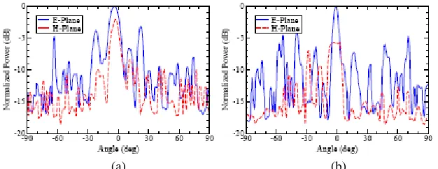
Simulated far field E-plane and H-plane at 19.5 GHz (a) and 21.5 GHz (b) of the optimized array by using ELVFEM/AMLFMA is shown in Figure 9. The CPU time consumed by ELVFEM/AMLFMA is 187961 seconds and the memory consumed is 6171MB (152738 unknowns). All the simulation work is finished on a workstation with Intel PIV 2.0 GHz processor and 10 GB memory.
4. MEASUREMENT AND ANALYSIS [13, 15–17, 19] 4.1. Far-field Patterns
The fabricated T/R antenna array is shown in Figure 10 and its far-field patterns are taken at 19.5 GHz in transmission and at 21.5 GHz in reception. Figure 11 shows the measured active patterns for the PA in transmission at 19.5 GHz and the LNA in reception at 21.5 GHz. The experiment results have a good agreement with the simulation results (Figure 9).
(a) (b)
Figure 9. Simulated far field E-plane and H-plane at 19.5 GHz (a) and 21.5 GHz (b).
4.2. Small-signal Gain
Small-signal measurements are performed with an HP 8510C vector network analyzer and are normalized to a free-space calibration performed through an array-sized aperture.
Figure 10. The fabricated T/R antenna array.
(a) (b)
Figure 11. Measured far-field E-plane and H-plane for the PA at 19.5 GHz (a) and LNA at 21.5 GHz (b).
performance of the other channel. The transmit array channel provides
−10.0 dB of gain at 19.0 GHz which is 3.0 dB above the passive array at 3.55 V and 1.73 A. The receive channel provides −3.8 dB of gain at 21.0 GHz with a 7.5 dB gain above the passive array at 4.00 V and 0.84 A. The presence or absence of bias to one channel has no effect on the gain of the opposing channel within the error of measurement.
Note that the difference in gain between the transmit and receive channel at the receive channel’s frequency of operation is separated by 25 dB. This isolation is critical to prevent the transmit channel from amplifying noise at the operation frequency of LNA.
to an impedance mismatch presented to the amplifier by wire bond inductance or the wire bond-transmission interface.
4.3. Saturated Power
Figure 13 shows the measured power at the output of the array as a function of the power present at the face of the array. Limitations imposed by MMIC instability prevent the acquisition of the maximum operating power. Maximum power out is measured to be 6 mW.
Figure 12. Measurement of the active array operating in full-duplex showing transmission response through the array as a function of frequency.
Figure 13. Output power at the face of the array versus input power at the face of the array.
5. CONCLUSION
In this paper,an active T/R antenna array work at different frequency is designed and fabricated. Because the array is electrically large at its work frequency,to design it efficiently a ELVFEM/AMLFMA method is applied to accomplish the simulation work and the GE algorithm is also used to optimize the array layout. Finally the array is fabricated according to the simulation results and the optimization results.
REFERENCES
1. Yuan,J.,Q.-Z. Liu,and J.-L. Guo,“Fast parallel algorithm for electromagnetic scattering problem via vector-FEM/MLFMA method,”Acta Electronica Sinica,Vol. 36,No. 3,520–526,2008. 2. Vandelay,A.,M. Von Nostrand,and K. Varnsen,“Signed-field
analysis of surface mode losses,” IEEE Microwave and Guided Wave Letters,1989.
3. Shih,Y. C. and T. Itoh,“Analysis of conductor-backed coplanar waveguide,” Electronics Letters,Vol. 18,538–540,June 1982. 4. Kumar,B. P. and G. R. Branner,“Design of unequally spaced
arrays for performance improvement,” IEEE Trans. Antennas Propagat.,Vol. 47,No. 3,511–523,1999.
5. Yan,K.-K. and Y. Lu,“Side-lobe reduction in array pattern synthesis using genetic algorithm,” IEEE Trans. Antennas Propagat.,Vol. 45,No. 7,1117–1122,1997.
6. Weile,D. S. and E. Michielssen,“Genetic algorithm optimization applied to electromagnetics: A review,” IEEE Trans. Antennas Propagat.,Vol. 45,No. 3,343–353,1997.
7. Haupt,R. L.,“An introduction to genetic algorithm for electromagnetics,”IEEE Antennas Propagat. Mag.,Vol. 37,No. 2, 7–15,1995.
8. Yuan,J.,Y. Qiu,J. Guo,Y. Zou,and Q.-Z. Liu,“Fast analysis of antenna mounted on electrically large composite objects,”
Progress In Electromagnetics Research,PIER 80,29–44,2008. 9. Guo,J. L.,J. Y. Li,and Q. Z. Liu,“Electromagnetic analysis of
coupled conducting and dielectric targets using mom with a pre-conditioner,”Journal of Electromagnetic Waves and Applications, Vol. 19,No. 9,1223–1236,2005.
10. Guo,J. L.,J. Y. Li,and Q. Z. Liu,“Analysis of antenna array with arbitrarily shaped radomes using fast algorithm based on VSIE,”
Journal of Electromagnetic Waves and Applications,Vol. 20,
No. 10,1399–1410,2006.
11. Qiu,Y.,J. Yuan,J. Tian,and Y.-J. Xie,“Antenna position optimal design for reducing interference,” 2004 International
Symposium on EMC Proceedings,689–693,June 2004.
13. Xiao,S.-Q.,J. Chen,X.-F. Liu,and B.-Z. Wang,“Spatial focusing characteristics of time reversal UWB pulse transmission with different antenna arrays,”Progress In Electromagnetics Research B,Vol. 2,223–232,2008.
14. Rocca,P.,L. Manica,and A. Massa,“An effective excitation matching method for the synthesis of optimal compromises between sum and difference patterns in planar arrays,” Progress In Electromagnetics Research B,Vol. 3,115–130,2008.
15. Naghshvarian-Jahromi,M.,“Novel Ku band fan beam reflector back array antenna,” Progress In Electromagnetics Research Letters,Vol. 3,95–103,2008.
16. Yuan,H.-W.,S.-X. Gong,P.-F. Zhang,and X. Wang,“Wide scanning phased array antenna using printed dipole antennas with parasitic element,”Progress In Electromagnetics Research Letters, Vol. 2,187–193,2008.
17. Abdelaziz,A. A.,“Improving the performance of an antenna array by using radar absorbing cover,” Progress In Electromagnetics Research Letters,Vol. 1,129–138,2008.
18. Cui,B.,J. Zhang,and X.-W. Sun,“Single layer microstrip antenna arrays applied in millimeter-wave radar front-end,”J . of
Electromagn. Waves and Appl.,Vol. 22,No. 1,3–15,2008.
19. He,Q.-Q.,Q. Wang,and B.-Z. Wang,“Conformal array based on pattern reconfigurable antenna and its artificial neural model,”J.
of Electromagn. Waves and Appl.,Vol. 22,No. 1,99–110,2008.
20. Zhai,Y.-W.,X.-W. Shi,and Y.-J. Zhao,“Optimized design of ideal and actual transformer based on improved micro-genetic algorithm,”J. of Electromagn. Waves and Appl.,Vol. 21,No. 13, 1761–1771,2007.