Compact Microstrip Lowpass Filter With Ultra-Wide Stopband
Using Patch Resonators and Open Stubs
Thulaseedharan K. Rekha1, *, Parambil Abdulla1, Paruthikkal M. Raphika2, and Puthenveetil M. Jasmine2
Abstract—A compact microstrip lowpass filter with ultra-wide stopband characteristics and high suppression level is presented. To achieve compact size and wide stopband suppression along with improved impedance matching, symmetrically loaded resonant patches, open stubs and stair shaped high impedance stub are introduced in the filter. The measurement results show good agreement with the simulations. The 3 dB cutoff frequency of the filter is 2.44 GHz. The stopband with attenuation level better than 22 dB is extended from 2.84 GHz to 16 GHz, hence an ultra-wide stopband with 6th harmonic suppression is achieved. The proposed filter has low insertion loss and high return loss in the passband, together with compact size of 0.257λg×0.148λg, whereλg is the guided wavelength at cutoff frequency. The relative stop bandwidth of the proposed design is identified to be 139.5%.
1. INTRODUCTION
Microstrip lowpass filters with compact size and wide rejection band are fundamental components in wireless communication systems to suppress unwanted high frequency harmonics. There are several configurations of microstrip components, which are often utilized for lowpass filter implementations. Among these, planar resonators are more important due to their compact size, ease of fabrication and integration with other microwave circuits. Lowpass filter design using conventional structures such as stepped impedance and open stubs suffers from gradual roll-off and narrow stopband bandwidth [1]. To increase the roll-off rate, more sections have to be added which increases the overall size of the filter. Compact design, low insertion loss and high return loss in the passband and high rejection in the stopband are necessary for filters used in modern communication applications. To meet these requirements, many methods are proposed [2–19]. A lowpass filter using stepped impedance and open stubs is proposed in [2] wherein semicircular stepped impedance resonators (SIRs) are used to make the structure more compact than conventional structures. Lowpass filter with in-line beeline compact microstrip resonant cell (CMRC) [3] and spiral compact microstrip resonant cell (SCMRC) structures [4] exhibit remarkable slow-wave and band-stop characteristics. But impedance matching in the passband and spurious suppression in the stopband are great challenges for periodic uniform CMRC’s, so tapered periodic CMRC is proposed in [5] for good impedance matching and spurious suppression. Double-folded SCMRC is proposed in [6] which has more compact dimensions and broader stopband than CMRC and SCMRC. Coupled line hairpin units can be used to design compact lowpass filter with wide rejection bandwidth [7–9], but these filters suffer from low roll-off rate and high return loss in the stopband. The return loss in the stopband is improved in circular SIRs loaded hairpin resonator cell [10]. Here, the stopband suppression level is only 10 dB. Another design technique of lowpass filter employs various forms of defective microstrip structures (DMS). A G-shaped DMS is proposed in [11] to get wide
Received 2 November 2016, Accepted 24 January 2017, Scheduled 27 February 2017
* Corresponding author: Thulaseedharan Kodiyattuvila Rekha ([email protected]).
stopband and selectivity at the cost of large physical size. Using transformed radial stubs, a new type of lowpass filter with ultra-wide band rejection and compact size is introduced in [12]. Defective ground structures (DGS) can be used to obtain wide stopband with high suppression level [13–15]. In [13], the proposed single DGS unit provides dual finite attenuation poles that can be independently controlled. High performance lowpass filter is designed in [14], by the use of coupled C-shape DGS and radial stub resonators for microwave mixer applications. A novel lowpass filter with elliptic shaped DGS and H-shape open stubs is presented in [15], but the stopband bandwidth of only 4.83 GHz is achieved. Using slit-loaded tapered microstrip resonator cell, a compact lowpass filter with sharp cutoff frequency is achieved in [16]. However, large layout area is required in this filter, and the stopband suppression level achieved is only 10 dB. Lowpass filter using cascaded multiple patch resonators is proposed in [17–19]. In [17], lowpass filter with sharp roll-off is achieved, but only second harmonic suppression could be reached. In [18], the filter has many advantages such as compact size and sharp roll off, whereas the stopband bandwidth is only up to 11 GHz. In [19], wide stopband is achieved by triangular and high-low impedance resonators, while the return loss in the passband is 10 dB.
The motivation of this paper is to design a new microstrip lowpass filter with compact size, ultra-wide stopband and high suppression level using an FR4 substrate. For this purpose, two different types of resonators, Resonator-1 and Resonator-2, are used in the design. To obtain wider stopband, open stubs are introduced in the structure. To improve the impedance matching in the passband of the filter, a novel high impedance stub arrangement is used, thereby the proposed filter satisfies wide stopband with high return loss and low insertion loss in the passband while retaining compact size. The filter is cost effective because it is fabricated using an FR4 glass epoxy substrate. From the proposed design, it is found that there is only optimum number of elements to maximize filter stopband and minimize passband losses. Measured results of the developed lowpass filter are in good agreement with the simulation ones, thereby proving the validity of the proposed approach.
2. THE LOWPASS FILTER DESIGN
The design procedure is carried out using the following steps.
2.1. Resonator-1 Design and Analysis
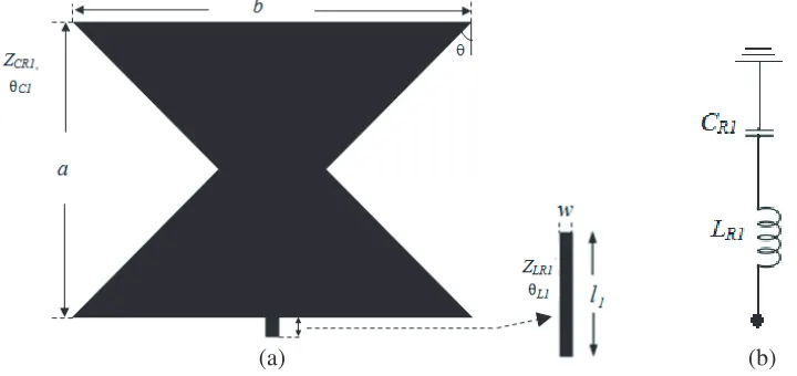
In the design of the proposed lowpass filter, the first step is to design Resonator-1. Figure 1(a) shows the geometry of Resonator-1 and (b) represents its LC equivalent circuit model. Resonator-1 is designed by using a high impedance straight stub connected in series with a low impedance polygonal patch, and these two form a quarter guided wavelength resonator and act as semi-lumped elements. The length and width of the high impedance stub are represented as l1 and w and the patch as a and b. The
(a) (b)
optimized dimensions of Resonator-1 are l1 = 0.3 mm, w= 0.2 mm, a= 4.4 mm, b= 6.0 mm,θ = 45◦. The high impedance stub acts as an inductor, LR1, and low impedance patch as a capacitor, CR1. The characteristic impedance of high impedance stub and low impedance patch is calculated using the equation in [1] for an FR4 glass epoxy substrate with relative dielectric constant of 4.4, thickness h of 0.8 mm and dielectric loss tangent of 0.02. The straight stub has a characteristic impedance ZLR1 of 120.5 Ω with electrical lengthθL1and that of the polygonal patchZCR1of 18.74 Ω, with electrical length, θC1, thereby satisfying the design considerations as,ZCR1 < Zo< ZLR1, where Zo is the characteristic impedance of 50 Ω feed line. The effective dielectric constant of the microstrip line of widthwand height h and the corresponding guided wavelength λgL are calculated at the cutoff frequency,fc1 of 2.53 GHz using equations in [1]. The equivalent inductanceLR1 can be calculated by using the expression,
LR1 =
ZLR1√εre
c l1 (1)
wherec is the velocity of light.
The guided wavelength λgc corresponding to the width of polygonal patch bis 61.23 mm at cutoff frequency 2.53 GHz. The value of capacitance for the dimension ais computed using the relation
CR1 =a/fc1λgcZCR1 (2)
The calculated values of the lumped elements of Resonator-1 areLR1 = 0.2079 nH, CR1= 1.515 pF.
Figure 2. Simulated S-parameters of Resonator-1 loaded on the main high impedance transmission line.
(a) (b)
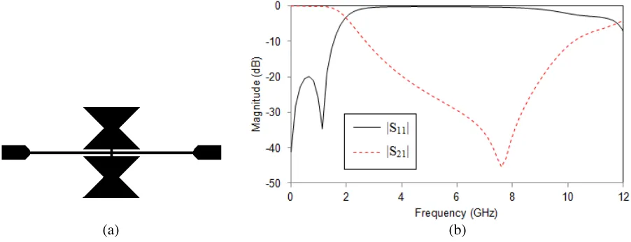
To understand the microstrip implementation of the filter structure, EM simulation software Zeland IE3D is used. The series LC resonator of Figure 1 is loaded to main transmission line having an impedance of 120.5 Ω. The simulated frequency response of Resonator-1 loaded on the main high impedance transmission line is shown in Figure 2. Resonator-1 creates a transmission zero located at about 5.97 GHz with attenuation level near 48.13 dB. Due to small value of resonance inductance LR1 of Resonator-1, transmission zero appears in the high frequency, which results in a wide stopband. A very low insertion loss in the passband is achieved by Resonator-1, but its transmission characteristics show gradual transition from passband to stopband.
The stopband bandwidth of Resonator-1 can be improved by loading the structure symmetrically on the main high impedance transmission line as shown in Figure 3. Compared to Figure 2, the stopband bandwidth and passband return loss of the filter are found greatly improved.
2.2. Resonator-2 Design
The next step is to design Resonator-2. Resonator-2 is a high impedance single stepped stub of characteristic impedance ZLR2 having electrical lengthθL2 connected in series with a triangular patch of impedance ZCR2 as 39.76 Ω. The layout of Resonator-2 is shown in Figure 4. The dimensions of the layout are l2 = 5.3 mm, w = 0.2 mm, a = 4.4 mm and d = 2.2 mm. The LC resonator is connected to main transmission line having an impedance of 120.5 Ω. One unit of Resonator-2 will create one transmission zero at 3.74 GHz with attenuation level near 30.909 dB. The cutoff frequency fc2 of Resonator-2 is 2.67 GHz.
Figure 4. The layout of Resonator-2.
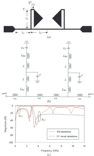
Connecting one more unit of Resonator-2 to the opposite side of Resonator-1, the selectivity of the filter can be improved. Its configuration, LC equivalent circuit and simulated characteristics are shown in Figures 5(a), (b) and (c), respectively. For the analysis of equivalent circuit, the single stepped stub l2 of Resonator-2 is divided as l2v, T-T and l2h. The vertical length of l2 is represented as l2v. Square shape T-T is the right-angle bend and l2h the horizontal length. The single stepped stub of Resonator-2 is placed at a distance lh1 from the end of main high impedance transmission line, and lh2 is the distance from the centre of main high impedance transmission line to the single stepped stub. The optimized dimensions of Figure 5(a) are l2v = 4.5 mm,l2h = 0.4 mm,T-T is 0.2×0.2 mm2, lh1 = 3.8 mm,lh2 = 4.1 mm.
(a)
(b)
(c)
Figure 5. (a) Structure of two units of Resonator-2. (b) LC equivalent circuit. (c) Characteristics of LC circuit and EM simulation.
LRv2 = 3.1199 nH, L= 0.176 nH, LRh2 = 0.4159 nH, CR2 = 0.68319 pF and C = 0.005159 pF. The LC circuit simulation result shown in Figure 5(c) is in good approximation with the EM simulated one.
(a) (b)
Figure 6. (a) Symmetrical structure of two units of Resonator-2. (b) SimulatedS-parameters.
increases, the stop bandwidth is improved with high suppression level. The roll-off rate and passband return loss of the filter are improved, with low insertion loss in the passband.
2.3. Cascaded Symmetrical Structure of Resonator-1 and Resonator-2
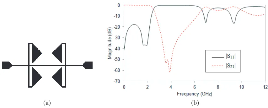
By suitably cascading symmetrical structure of Resonator-1 and two units of Resonator-2 on the main high impedance transmission line, the filter performance is greatly improved. Figure 7 shows the geometry and frequency response of the filter with symmetrical arrangement of Resonator-1 and two units of Resonator-2.
(a) (b)
Figure 7. (a) Combined symmetrical structure of Resonator-1 and Resonator-2. (b) Simulated S -parameters.
2.4. Cascaded Structure with Open Stubs
In many practical applications, a lowpass filter with wide stopband and high suppression level is necessary. The bandwidth of the combined filter can be greatly enhanced by connecting open stubs on both sides of the resonators. The open stub produces a transmission zero when the physical length of the stub is less than quarter wavelength. The filter using open circuited stub at both ends of the high impedance main transmission line exhibits better stopband characteristics.
Figure 8 shows the structure of open stubs whereZosandθosrepresent the characteristic impedance and electrical length, respectively. The length and width of the open stub are p and q, respectively. For the straight stub, the equivalent capacitance can be derived by using [1]. Each open stub acts as a shunt capacitor to the ground. At high frequencies, the capacitive reactance decreases, and open stub acts as a short circuit to the ground. This shorts out transmission and causes attenuation peak in the stopband which suppresses the higher frequency harmonics and extends the stopband. The optimized values ofp and q are 0.8 mm and 10 mm, respectively.
Figure 8. Structure of open stub. Figure 9. Structure of cascaded symmetrical Resonator-1, Resonator-2 and open stubs.
Figure 9 shows the cascaded structure of symmetrical Resonator-1, Resonator-2 and open stubs. Resonator-1 is placed between two units of Resonator-2, and these three units are symmetrically loaded on the centre of a high impedance main transmission line, together with two open stubs, which are connected at both ends of high impedance main transmission line. Figure 10(a) shows the LC equivalent circuit of the cascaded symmetrical Resonator-1, Resonator-2 and open stubs. LR1 represents the equivalent inductance of high impedance straight stub of Resonator-1, and CR1 is the capacitance between the microstrip polygonal patch and the ground plane. CR2 represents the capacitance between microstrip triangular patch and the ground plane, and COS is the capacitance of the open stub and the ground plane. The capacitance Cc is formed by the capacitive coupling between the polygonal and triangular shape patches, and its value is calculated using [1]. At high frequency values, the inductance of main high impedance line blocks transmission by having infinite series reactance, whereas the capacitance of open circuited stub shorts out transmission by having infinite shunt susceptance. The calculated values of the lumped elements of the proposed lowpass filter design are LH1 = 2.6346 nH, LH2 = 2.8426 nH, LR1 = 0.2079 nH, LRv2 = 3.1199 nH, L = 0.176 nH, LRh2 = 0.4159 nH, CR1 = 1.515 pF, CR2 = 0.68319 pF, C = 0.005159 pF, Cos = 0.4343 pF and Cc = 0.03837 pF. Figure 10(b) shows the LC and EM simulation results of the cascaded structure which are in good approximation with each other. As seen in figure, enhanced stopband performance is achieved under the combined effect of two types of resonators and open stubs. The cutoff frequency of the filter is 2.64 GHz.
2.5. Efforts for Improving Impedance Matching in the Passband
(a)
(b)
Figure 10. (a) LC equivalent circuit of cascaded symmetrical Resonator-1, Resonator-2 and open stubs. (b) Characteristics of EM and LC circuit simulation.
The insertion loss in the passband of the filter is less than 0.62 dB from DC to 1.7 GHz, and the return loss is only 14.8 dB. By increasing the length of high impedance single stepped stub of Resonator-2 (l2), (only the length of l2 in horizontal direction is increased) the characteristics of the filter have been changed. Figure 12 shows the reflection and transmission characteristics of the filter for different values ofl2.
Figure 11. SimulatedS-parameters of the cascaded structure of symmetrical Resonator-1, Resonator-2 and open stubs.
(a)
(b)
Figure 12. Simulated S-parameters of the lowpass filter for various values of l2. (a) Reflection characteristics. (b) Transmission characteristics.
Figure 13. Simulated S-parameters of the filter for inductive stub structure of Resonator-2 as stair shaped and single step forl2 = 6.7 mm.
Figure 14. Structure of the proposed lowpass filter.
as single step and stair shape of length l2 as 6.7 mm, between main high impedance transmission line and triangular patch. For a single stepped resonator, the filter suffers from poor impedance matching in the passband and spurious signals arising in the stopband. These two drawbacks of the filter can be eliminated by using the stair-shaped high impedance stub. By the introduction of stair-shaped high impedance stub, the impedance matching as well as stopband suppression level of the filter is improved to a great extent.
The return loss values in the passband are improved from 14.8 dB to 18.5 dB, and thereby the insertion loss in the passband decreases from 0.62 dB to 0.5 dB. Due to increase in inductance value of Resonator-2, the cutoff frequency of filter decreases, and the value in the proposed design is 2.44 GHz. Figure 14 shows the final structure of the proposed lowpass filter, where the single step high impedance inductive stub of Resonator-2 is modified as stair shape of increasing step size, and Figure 15 shows the simulated characteristics of the final filter.
Figure 15. Simulated S-parameters of the proposed filter.
(a)
(b)
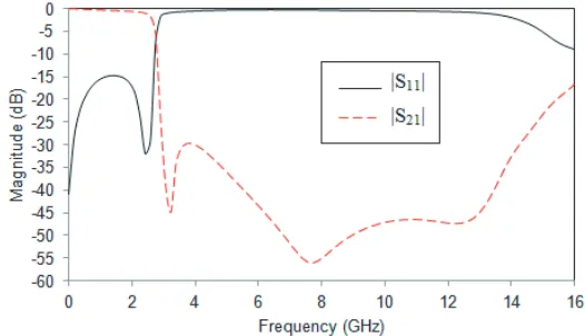
Figure 16. (a) Photograph of the proposed filter. (b) Measured and simulated S-parameters of the proposed filter.
The phase velocity of a lossless structure can be expressed as,
νp = √1
LC (3)
Increasing the length of the high impedance stub by introducing stair-shaped design enhances the effective inductance, and the small value of the coupling gap g between the resonators improves the effective capacitance of the filter. By cascading the resonators, equivalent inductance and capacitance values increase, which correspond to decrease in the phase velocity, and thus a slow wave effect is achieved. A wide stop bandwidth up to 16 GHz (at 22 dB suppression level) is obtained, due to multiple transmission zeros contributed by two types of patch resonators together with two open stubs. Cutoff frequency of the filter is 2.44 GHz, with low insertion loss and good impedance matching in the passband.
3. FABRICATION AND MEASUREMENT RESULTS
The filter structure is fabricated on an FR4 substrate with relative permittivity 4.4, dielectric loss tangent 0.02 and thickness 0.8 mm. A photograph of the fabricated filter structure along with SMA connectors is shown in Figure 16(a). The measurement is carried out using PNA E8362B Vector Network Analyzer. The measurement results are in good agreement with the simulated ones as illustrated in Figure 16(b). The measured results show that the 3 dB cutoff frequency of the proposed filter is 2.44 GHz. The minimum return loss is better than 17.74 dB over the entire passband and the suppression level better than 22 dB from 2.85 GHz to 16 GHz. The suppression level of 31 dB is achieved from 2.94 GHz to 13.04 GHz. Thus wide stopband rejection is obtained in 77% of overall stopband bandwidth. The insertion loss in the passband is less than 0.67 dB from DC to 1.7 GHz. The higher value of insertion loss in the passband of the filter is due to the high dielectric losses of the FR4 substrate at microwave frequencies. The return loss in the stopband is very close to 0 dB and nearly 4.3 dB at the end of the stopband. The roll-off rate of the structure is 67.27 dB/GHz at 40 dB suppression level. The physical size of the filter is only 17.4 mmx10 mm, which corresponds to a normalized circuit size of 0.257λg×0.148λg, where λg is the guided wavelength at the cutoff frequency. The relative stop bandwidth (RSB) of the proposed filter is 139.5%.
The measured and simulated group delays in Figure 17 show good approximation. The group delay is almost flat in the passband with maximum variation of 0.2 ns. There is a significant increase in group delay when the frequency approaches the cutoff frequency of the filter.
Figure 17. Measured and simulated group delay characteristics of the proposed lowpass filter.
Table 1. Comparison of parameters of similar works. Ref. Return loss (dB) Cutoff frequency (GHz) Stopband (GHz @ dB)
Substrate/dielectric loss tangent Substrate dielectric constant/ height (mm)
[2] 15 5.2 (5.5 to 14 @ 20) ArlonAD430/0.003 4.4/0.635
[5] 19.5 1.3 (1.75 to 13 @ 19) PTFE/0.0035 2.65/1.5
[8] 16.3 0.5 (0.5 to 4.5 @ 20) FR4/0.022 4.3/1.58
[9] 17 1.2 (1.91to 10.35 @ 15) Roger/0.0027 3.5/0.762
[10] 13 2.0 (2.5 to 16 @ 10) RT duroid/0.0009 2.2/0.254
[11] 10 3.17 (3.4 to 10 @ 25) PTFE/0.0027 2.65/1.0
[15] 20 4.5 (5.2 to 10 @ 32) Taconic TLC/0.003 3.2/0.787
[16] 10.67 1.78 (1.86 to 10.71 @ 10) RT duroid/0.0009 2.2/0.508
[17] 20 5.55 (5.88 to 11.8 @15) FR4/0.02 4.4/1.6
[18] 17 2.28 (2.49 to 11 @ 23) FR4/0.02 4.4/1.6
[19] 10 1.5 (1.55 to 13 @ 15) RT duroid/0.0009 2.33/0.7874
This work 17.74 2.44 (2.94 to 13.04 @ 31)
(2.85 to 16 @ 22) FR4/0.02 4.4/0.8
4. CONCLUSION
A novel microstrip lowpass filter symmetrically loaded with multiple patch resonators and open stubs has been studied. The detailed analysis of LC equivalent circuit of the filter is conducted. The measured 3 dB cutoff frequency of the filter is 2.44 GHz, which is in good agreement with the simulated frequency. Results show that the proposed lowpass filter is able to suppress better than sixth harmonics referred to 22 dB suppression level, together with compact size, good selectivity and impedance matching. With these good features, the proposed lowpass filter can be introduced in wireless LAN, L-band applications and Bluetooth networking applications.
REFERENCES
1. Hong, J. S. and M. J. Lancaster, Microstrip Filters for RF/Microwave Applications, Wiley, New York, 2001.
2. Wang, L., H. C. Yang, and Y. Li, “Design of compact microstrip low-pass filter with ultra-wide stopband using SIRs,”Progress In Electromagnetics Research Letters, Vol. 18, 179–186, 2010. 3. Zhang, F., J. Z. Gu, C. Y. Gu, L. N. Shi, C. F. Li, and X. W. Sun, “Lowpass filter with in-line
beeline CMRC,”IET Electronics Letters, Vol. 42, No. 8, 472–474, 2006.
4. Gu, J. and X. Sun, “Compact lowpass filter using spiral compact microstrip resonant cells,” IET Electronics Letters, Vol. 41, No. 19, 1065–1066, 2005.
5. Li, L., Z.-F. Li, and Q.-F. Wei, “Compact and selective lowpass filter with very wide stopband using tapered compact microstrip resonant cells,”IET Electronics Letters, Vol. 45, No. 5, 267–268, 2009.
6. Ke, L., M. Zhao, Y. Fan, Z. Zhu, and W. Cui, “Compact lowpass filter with wide stopband using novel double-folded SCMRC structure with parallel open-ended stub,”Progress In Electromagnetics Research Letters, Vol. 36, 77–86, 2013.
7. Wei, F., L Chen, and X-W Shi, “Compact lowpass filter based on coupled-line hairpin unit,” IET Electronics Letters, Vol. 48, No. 7, 379–381, 2012.
9. Chen, X., L. Zhang, Y. Peng, Y. Leng, H. Lu, and Z. Zheng, “Compact lowpass filter with wide stopband bandwidth,”Microwave and Optical Technology Letters, Vol. 57, No. 2, 367–371, 2015. 10. Yang, M. H., J. Xu, Q. Zhao, L. Peng, and G. P. Li, “Compact, broad stopband lowpass filters
using SIRs-loaded circular hairpin resonators,” Progress In Electromagnetics Research, Vol. 102, 95–106, 2010.
11. Cao, H., W. Guan, S. He, and L. Yang, “Compact lowpass filter with high selectivity using G-shaped defected microstrip structure,” Progress In Electromagnetics Research Letters, Vol. 33, 55–62, 2012.
12. Ma, K. and K. S. Yeo, “New ultra-wide stopband low-pass filter using transformed radial stubs,” IEEE Transactions on Microwave Theory and Techniques, Vol. 59, No. 3, 2011.
13. Li, Y., H.-C. Yang, and S.-Q. Xiao, “Lowpass filter with wide stopband and sharp skirt using novel defected ground structure,”Progress In Electromagnetics Research Letters, Vol. 41, 185–191, 2013. 14. Belbachir, A. K., M. Boussouis, and N. A. Touhami, “High-performance LPF using coupled C-shape DGS and radial stub resonators for microwave mixer,”Progress In Electromagnetics Research Letters, Vol. 58, 97–103, 2016.
15. Chen, X. Q., R. Li, S. J. Shi, Q. Wang, L. Xu, and X. W. Shi, “A novel low pass filter using elliptic shape defected ground structure,”Progress In Electromagnetics Research B, Vol. 9, 117–126, 2008. 16. Hayati, M. and A. Lotfi, “Elliptic function lowpass filter with sharp cutoff frequency using slit-loaded tapered compact microstrip resonator cell,”IET Electronics Letters, Vol. 46, No. 2, 143–144, 2010.
17. Raphika, P. M., P. Abdulla, and P. M. Jasmine, “Compact lowpass filter with a sharp roll-off using patch resonators,”Microwave and Optical Technology Letters, Vol. 56, No. 11, 2534–2536, 2014. 18. Raphika, P. M., P. Abdulla, and P. M. Jasmine, “Planar elliptic function lowpass filter with sharp
roll-off and wid stopband,” Microwave and Optical Technology Letters, Vol. 58, No. 1, 133–136, 2016.