N A N O E X P R E S S
Open Access
Evaluation of optical and electronic properties of
silicon nano-agglomerates embedded in SRO:
applying density functional theory
Néstor D Espinosa-Torres
*, David Hernández-de la Luz, José Francisco J Flores-Gracia, José A Luna-López,
Javier Martínez-Juárez and Diana E Vázquez-Valerdi
Abstract
In systems in atomic scale and nanoscale such as clusters or agglomerates constituted by particles from a few to less than 100 atoms, quantum confinement effects are very important. Their optical and electronic properties are often dependent on the size of the systems and the way in which the atoms in these clusters are bonded. Generally, these nanostructures display optical and electronic properties significantly different to those found in corresponding bulk materials. Silicon agglomerates embedded in silicon rich oxide (SRO) films have optical properties, which have been reported to be directly dependent on silicon nanocrystal size. Furthermore, the room temperature photoluminescence (PL) of SRO has repeatedly generated a huge interest due to its possible applications in optoelectronic devices. However, a plausible emission mechanism has not been widely accepted in the scientific community. In this work, we present a short review about the experimental results on silicon nanoclusters in SRO considering different techniques of growth. We focus mainly on their size, Raman spectra, and photoluminescence spectra. With this as background, we employed the density functional theory with a functional B3LYP and a basis set 6-31G* to calculate the optical and electronic properties of clusters of silicon (constituted by 15 to 20 silicon atoms). With the theoretical calculation of the structural and optical properties of silicon clusters, it is possible to evaluate the contribution of silicon agglomerates in the luminescent emission mechanism, experimentally found in thin SRO films.
Keywords:Nano-agglomerates; Silicon clusters; Silicon rich oxide; Luminescence; HRTEM; DFT
Background
Small silicon clusters can be obtained, for instance, when using photochemical etching treatment and pulsed laser evaporation method which in turn show also photolumines-cence (PL). Nevertheless, such small silicon clusters are short-lived intermediate species, and it is very difficult to control the number of atoms in the Si clusters formed. On the other hand, some silicon clusters have been prepared by organic synthesis methods, and a similarity of the PL and absorption spectra to those measured in porous Si (p-Si) has been pointed out. With respect to the latter material, it is currently agreed that the quantum confinement effects and the hydro-gen saturation (surface effects) of Si nanocrystallites play key roles in the origin and mechanism of PL in p-Si where
strong visible PL is observed when it is fabricated by electro-chemical anodization [1]. Besides, their optical and electronic properties have caught much attention from the perspective of solid-state physics and its application to optical devices [2,3].
Kanemitsu and co-workers [4,5] and Furukawa et al. [6] synthesized several kinds of Si clusters, Si backbone polymers, network polymers, and planar siloxane struc-tures and studied their optical properties to understand the dimensional effects of Si-based nanostructures such as p-Si. In the chain clusters and polymers, sharp PL bands were observed with very small Stokes shifts. On the other hand, following the line of nanostructures with Si clusters, we find that such structures which have generated great interest is the silicon rich oxide (SRO) thin film; this material exhibits optical properties in the same manner to p-Si, but it is significantly less chem-ically reactive than p-Si.
* Correspondence:[email protected]
Instituto de Ciencias, Centro de Investigaciones en Dispositivos Semiconductores, Benemérita Universidad Autónoma de Puebla, C.U. Edif. 103 C-D, Col. San Manuel, Puebla Pue., C.P. 72570, Mexico
Si-nanocrystals (Si-nCs) embedded in dielectric matri-ces such as silicon dioxide exhibit unique optical and electrical properties which are determined by quantum size and Coulomb blockade effects [2]. Si-nCs can emit and absorb light at energies which can be controlled by their sizes, i.e., their gaps can be tuned. This latter funda-mental property of Si-nCs is very useful in third-generation solar cells [7].
Commonly, SRO is considered as a multi-phase material constituted by a mixture of silica (SiO2), off-stoichiometric oxides (SiOx,x< 2), and elemental silicon. After thermal
treat-ment at temperatures above 1,000°C, the off-stoichiometric oxides, SiOx (x< 2), react to produce silicon
nanoclus-ters, structures with different oxidation states with or without defects, and silica [8]. Silicon nanocrystals and silicon agglomerates have been characterized in SRO films employing transmission electron microscopy (TEM), high-resolution transmission electron micros-copy (HRTEM), energy-filtered transmission electron microscopy (EFTEM), X-ray diffraction (XRD), and atomic force microscopy (AFM) [9] as characterization techniques. The formation, shape, and size of Si-nCs depend on the excess silicon and annealing parameters (time and temperature) and also on the type of carried gas used to grow nanostructures.
According to Raghavachari and Rohlfing [10], the be-havior of small-sized silicon clusters is frequently corre-lated with the trend of binding energy per atom as a function of cluster size. In this type of systems, the elec-tronic configuration corresponding to both a single atom and a complex of atoms in the cluster is a determining factor in the cluster stability [11].
Over the past 20 years, medium-sized silicon clusters Sin (n> 10) have attracted much attention both
experi-mentally [12] and theoretically [13]. Considerable effort has been devoted to determine the ground-state geomet-ric structures, namely the global minima as a function of the cluster sizen. Forn≤7, the global minima are firmly established by bothab initiocalculations and Raman/in-frared spectroscopy measurements, whereas for n≤12 the global minima based only on ab initio calculations [14-16] are well accepted.
For 13≤n≤20, an unbiased search for the global minima has been undertaken based on either the genetic algorithm coupled with semi-empirical tight-binding (TB) technique [17] or the single-parent evolu-tion algorithm coupled with density funcevolu-tional (DF), TB, and density functional theory (DFT) methods [18,19]. Establishing successfully the geometry corre-sponding to the global minimum energy is a critical step for a further reliable evaluation of the optical and structural properties, and thereby it contributes prop-erly to the understanding of the undprop-erlying mecha-nisms of luminescence.
It is well-known that crystalline silicon (c-Si) has an indirect band gap, which means that every optical transi-tion must be accompanied by the creatransi-tion or annihila-tion of a phonon. Besides, this material presents an optical disadvantage attributed to low band gap valueEg,
c-Si= 1.12 eV at room temperature (RT), corresponding to a wavelength λg,c-Si= 1,107 nm. This fact leads to the radiation emitted by, for example, a light-emitting diode (LED) made of c-Si which corresponds to the infrared emission and then it is non-visible by the human eye.
However, by using nanoscaled silicon structures, the optical disadvantage can be overcome, because of the presence of radiative optical transitions brought about in quantum confined states of Si nanostructures which generate visible radiation, but the disadvantage of the in-direct band gap still remains. Average PL decay times τPLfor Si-nCs with diametersd~ 3.4 nm are reported to be in the order of 100 to 500μs at RT [20].
Broadly, the SRO can be obtained by different tech-niques; however, the low-pressure chemical vapor depos-ition (LPCVD) technique is frequently used because it results a simple method that easily allows the controlled fluctuations of silicon excess. In this technique, the par-tial pressure ratio caused by the flow of reactive gases, defined as Ro =P(N2O)/P(SiH4), is used to determine the silicon excess. For example, for Ro = 3, we have a sil-icon excess of 17 at.%, and Ro = 100 is used to obtain stoichiometric silicon dioxide. When SRO films are ob-tained by LPCVD technique, the most intense light emission observed corresponds to films with approxi-mately 5 at.% silicon excess as reported, although silicon nanocrystals were not observed in such films [21].
It is possible that small-sized silicon agglomerates (Sin,
some host material like SRO, represent a high potential barrier for carriers (electrons or holes). Such a barrier is often referred to as a confining quantum potential that mainly defines the energy spectrum of the Si-nCs.
There is a large uncertainty in the calculated values of the optical gaps as a function of Si-nC diameter. We can mention two factors influencing the accuracy of the optical gap measurements as follows: First, the nano-crystals which are studied by different research groups have been prepared using different techniques. This fact leads to nanocrystals having different surroundings, surface bonds, and shapes, all of which could lead to scatter in the experimental data. Second, it is difficult to determine exactly the dot sizes and the size distribution in luminescent agglomerate of nanocrystals. Theoretic-ally, the problem persists mainly due to the difficulty to define an appropriate parameter for determining the diameter. For simplicity, a spherical geometry is used in most of the models suggested, since the actual shape of the agglomerates formed and considered as a molecule is totally irregular.
As has been reported in the literature, we can employ a space-filling model, for visualizing the effective shape and relative dimensions of the molecule, in particular, the region of space occupied by it. This model also known as CPK one, is a type of three-dimensional mo-lecular model where the atoms are represented by spheres whose radii are proportional to the radii of the atoms and whose center-to-center distances are propor-tional to the ones between the atomic nuclei, all in the same scale. We can correlate CPK area and CPK volume, obtaining the diameterD(Å) through the equation [9]:
6CPKvolume CPKarea ¼
64 3πðD=2Þ3 4πD=2Þ2
The motivation of this work is to present a theoretical study of the optical and electronics properties of Si-nCs which are embedded in SRO structures regardless of the technique used to fabricate such structures. For this, we review firstly some important experimental results about the measurements of the structural and optical proper-ties carried out on SRO samples grown by different tech-niques. The aim of this review is twofold; on the one hand, we show relevant information in relationship to actual quantification of Si-nCs about their size, electro-magnetic range of emission, molecular structure, and important parameters which are responsible for making variations of these properties. On the other hand, we take this experimental information as background in order to focus correctly our theoretical research pre-dicted by using the DFT method corresponding to atomic composition of different silicon isomers sug-gested simulating the Si-nC embedded in SRO films.
This paper is outlined as follows: the‘Methods’section includes the elemental analytical expressions of energy in nanocrystals. In the ‘Results and discussion’section, we present two parts: in the first one, we show and dis-cuss the experimental identification and quantification of silicon nanocrystals in SRO films, and then we present and discuss the theoretical results about the structural and optical properties of silicon clusters using DFT method. Finally, the last section presents the conclusions.
Methods
Elemental analytical expressions of energy in nanocrystals Different proposals of elemental models to get analytical expressions of energy of Si-nC are found in the litera-ture, which pretend to explain correctly the energy spectrum of this type of nanostructures. However, this task is not easy because of the complexity associated to these nanoclusters which do not have a well-defined geometry and their composition is nonhomogeneous. Among the several geometries suggested for studying the optical properties of Si-nCs, we find that the spher-ical geometry is predominantly accepted as a first ap-proximation to understand, to a certain degree, the emission mechanisms in the nanocrystals. In order to obtain the electronic states in a nanocrystal, with a spherical shape, its Hamiltonian, H¼−2ℏm2∇2þU rð Þ,
must be solved. Gaponenko [28] used spherical coordi-nates r, θ, and φ to solve this Hamiltonian, where the total potential energy U(r) of the electron inside the spherical region has radial symmetry. By standard methods, the eigenfunctions of this Hamiltonian are found to be Ψn;l;mðr;θ;φÞ ¼un:lrð Þr Ylmðθ;φÞ where n is
the principal quantum number, l is the orbital number, and m is the magnetic number. Here,Yl,m(θ, φ) are the
spherical functions. With these solutions Ψn,l,m(r, θ, φ)
when introduced in the Hamiltonian, we arrive to the
equation−2ℏm2d2u
dr2þ U rð Þ þ ℏ 2
2mr2l lð þ1Þ
h i
u¼Eu. The en-ergy values of the electronic states in a spherical nano-crystal are obtained as a solution to this equation, when the potential U(r) is considered as infinitely high. The
energy spectrum is given by Enl ¼
ℏ2χ2
nl
2ma2, where a= 0.543 nm is the lattice constant of Si and χnl are the
roots of the spherical Bessel functions.
On the other hand, inside the Si-nCs, the electrons and holes are interacting through Coulomb attraction; this fact leads to the formation of excitons. An exciton is known as a bound pair formed by an electron and a hole interacting by Coulomb force forming a hydrogen-like system. When the Bohr radius of the exciton is larger than the size of the nanocrystal, it takes place a quantum confinement. Considering that silicon dioxide surrounds
the silicon nanocrystals, and due to it forms a high po-tential barrier (approximately 9 eV), the excitons are confined within the volume of the nanocrystal. This causes drastic changes in both the electronic band struc-ture and the emission spectrum.
Considering the presence of excitons in the medium and the effects of polarization due to the dielectric oxide sur-rounding the Si-nC, it can be shown that the Hamiltonian in the effective mass approximation is given by H¼−
e2
εjre−rhj−
ℏ2 2
1
me∇ 2
eþm1h∇ 2
h
h i
þpolarization terms, whereεis the dielectric function of the nanocluster, andme andmh are the effective masses of electron and hole, respectively. Owing to the dielectric function which varies in the cluster by virtue of the nonhomogeneous composition in the sur-rounding medium, it gives rise to an image charge effect on the electron, i.e., polarization effects which must be added to its total energy as shown qualitative in the last term of
H. More precisely, the polarization terms refer to the effect of image charge on carriers due to the difference in dielec-tric constants of the sphere and the surrounding medium. The contribution of polarization terms to the original po-tential energy U0(r), by and large, is too complex. So, the total potential energy now becomes U(r) =U0(r) +Vsp(r) whereVsp(r) is often referred to as a self-polarization term. This term describes an interaction between the electron and its image charge, emerging due to the charge polarization on the boundary between the Si-nC and its dielectric surrounding. It can be represented as [10]Vspð Þr
¼e2ðεs−εpÞ 2εsR
X∞
l¼0 lþ1
lεsþðlþ1Þεd
r2l
R2l, whereεsandεdare the static
di-electric constants of bulk silicon and the didi-electric sur-rounding matrix, respectively. It is found that an analytical approximated expression for the lowest eigenvalue of the Hamiltonian including the total energy potential (i.e., the first excited electronic state) is [29]
E≅EG−1:8e
2
εR þ
ℏ2π2 2R2
mhþme
memh
: ð1Þ
whereEGis the bulk band gap and Ris the size of the Si-nC. The first term proportional toR−1is the Coulomb term, and the second one proportional toR−2is the shift as a result of quantum localization of electrons and holes (quantum confinement). Equation 1 is possible to establish because the correlation between electron and hole positions, induced by the Coulomb interaction, is not enough strong. Independently of confinement ener-gies for electrons and holes, the major effect is additive.
The first theoretical calculation for semiconductor nanoparticle energy is based on‘effective mass approxi-mation’ (EMA), which was proposed in 1984 by Brus [30]. This approximation allows us to obtain the exciton energy when it is confined to a spherical volume of the
crystallite in terms of electron and hole effective masses, and it can be expressed as
E¼EGþℏ
2π2
8R2
mhþme
memh
− 1:786e2
4πε0εrR2 ð 2Þ
ε0 is the permittivity of vacuum and εr is the relative permittivity of Si-nC. Four years later, in 1988 Kayanuma [31] accounted for the electron-hole spatial correlation effect and modified the Brus equation, including a nega-tive term proportional to Rydberg energy.
For very small clusters, there is a large difference be-tween the electron effective mass and the hole one which is much heavier. This fact yields that (mh+me)/
memh≈1/me. On the other hand, for very small nano-agglomerates, it is found that
ΔE≈ h
2π2
2meR2 ð
3Þ
where ΔE=E−EG. Apart from this model, many
others have been developed with several refinements. The EMA is a rough approximation which assumes the cluster (or nano-agglomerated) to be in a well of infinite potential energy where the Coulomb terms are excluded from the analysis. Brus [32] improved the original model including the Coulomb terms taking into account the effect of the dielectric constant of the matrix on the exciton binding energy and using finite potential wells for calculating energy states. Other EMA models were developed by Kayanuma [31] and Kayanuma and Momiji [33] using quantum confinement finite potentials for mod-eling clusters with cylindrical and spherical geometries.
The extension of Efros and Efros [22] model suggested by Brus [32] and Kayanuma [31] to include Coulombic energies and correlation effects allows us to derive an expression that models the energies and provides a rea-sonable guide to the cluster size as a function of EG, in
such case the energy is
E Rð Þ ¼EGþh
2π2
2R2
mhþme
memh
−1:ε786e2 rR2
þ0:285ER ð4Þ
whereERis the Rydberg energy for the semiconductor in bulk and is given by [34] ER¼ε2 13:606m0
rððmeþmhÞ=memhÞ eV. In Equation 4, the terme2is the Coulombic term and 0.248
At first glance, it may be redundant to present the above theory related with analytical expressions of en-ergy of Si-nCs, but we must keep in mind that these formulae have frequently used to estimate emission radiation in Si-nC. Nevertheless, their predictions are limited since the theoretical models ignore a lot details that in practice the Si-nCs present themselves. It opens the opportunity to establish a new formalism capable of explaining in depth the underlying physical mechanisms involved in the radiative emission of Si-nCs.
Results and discussion
Experimental identification and quantification of silicon nanocrystals in SRO films
Identification of vibrational modes in Si-nCs by Raman spectroscopy
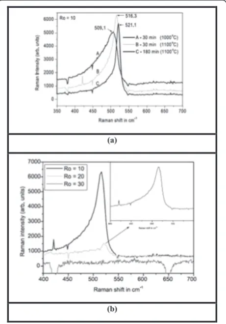
Raman's effect takes place due to the interaction of op-tical and vibrational oscillations and results in a variation in vibrational energy of molecule. A phonon is created (anti-Stokes process) or annihilated (Stokes process) dur-ing the Raman scatterdur-ing. Raman spectroscopy as a fast and nondestructive method is recurrently used to characterize the Si nanocrystals. Starting from the shape and the peak position of the first-order Raman scattering band, we can determinate the composition of the nano-crystal, do the estimation of the size of the nanocrystals, corroborate the evolution of the stress on nanocrystals, and estimate the amorphous to crystalline ratio (phase changes). Figure 1 displays the experimental results obtained for SRO thin films deposited by LPCVD tech-nique. Amorphous silicon (a-Si) as well as c-Si can be identified by Raman spectroscopy [35]. A broadband around 480 cm−1 is typically associated to a-Si, while bulk silicon has a sharp peak around 521 cm−1. For Si-nCs, their peak shifts to smaller wavenumbers, as a func-tion of decreasing size; it has been extensively associated to quantum confinement effects. For pre-annealed films with Ro = 20 and 30, no Raman peaks for Si nanocrystals were observed, but for Ro = 20, a broadband at 485 cm−1 indicates the presence of a-Si.
Fascinatingly, the sample with Ro = 10 displays a strong Raman peak for Si nanocrystals at 509.1 cm−1 (Figure 1a, the lower curve), indicating that for films with a high Si excess during the 30 min of pre-annealing Si nanocrystals were already formed. After 30 min of an-nealing at 1,100°C (Figure 1b), a small Raman peak around 521.1 cm−1 for Ro = 20 is observed (the middle curve and see inset on Figure 1b), while for Ro = 30 (the lower curve), no peaks were found. Further heating treatment for another 150 min proceeds with this trend; for Ro = 20, an increase of the intensity is observed, whereas for Ro = 30, no characteristic peaks for Si phases were found.
[image:5.595.307.538.90.420.2]Structural characterization of Si-nCs by X-ray diffraction The theory and mathematical representation of XRD by a simple lattice was studied in detail by Laue [36] and Bragg [29], and it is very known that XRD lines of the stressed materials exhibit asymmetrical and broadened line profiles depending on the magnitude of the stress [37]. Therefore, misinterpretation may arise from the fact that both stress and the decrease in coherence length can cause broadening. The method of integral breadths, described by Santra et al. [38] and Warren and Averbach [39] can be used to calculate the effect of both finite grain size and lattice distortion simultaneously. Both methods require the precise measurements of sev-eral diffraction lines. In the case of Si nanocrystals em-bedded in dielectric matrices, Si(111), (220), and (311) peaks are usually observed. However, the signal to the Bragg peaks of Si (220) and (311) sometimes is weak to perform these methods accurately. Figure 2 displays XRD results obtained for SRO10 film (an SRO film with Ro = 10) deposited by LPCVD technique. The average size found was from 4.8 to 5.0 nm after 30 and 180 min
(annealing times). The broad peak in 21° corresponds to a-SiO2, whereas peaks in 28.4° and 47.3° are due to Si (111) and (220), respectively. Incipient peak in 43° could be Si (311).
Detection of Si-nC by energy-filtered transmission electron microscopy
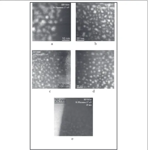
By using EFTEM, spatial resolution down to 1 nm can be succeeded. However, EFTEM has no limitations re-lated to the crystallinity of the Si-nCs and can detect both amorphous and crystalline nanoclusters. Moreover, high energy resolution of EFTEM can make it possible to distinguish Si and SiO2plasmon energies.
The raw images obtained from EFTEM measurements were slightly contrasted, and the subtraction of the contribution from SiO2 background by yielding a well-defined Si nanocluster was applied. EFTEM is advanta-geous when analyzing a number of specimens in a short time. Thus, EFTEM is more appropriate for statistical analysis.
Figure 3 displays images obtained for SRO films de-posited by LPCVD with different concentrations and an-nealing times. Figure 3a,b corresponds to Ro = 10 after thermal treatment during 1 h, in two scales; Figure 3c,d corresponds to Ro = 20, with treatment of 1 h, consider-ing two different temperatures; and finally, Figure 3e corresponds to the image of SRO30, after annealing at 1,100°C during 1 h.
Dimensional estimation of Si-nCs by high-resolution transmission electron microscopy
After Voyles [40] first discerned the distribution of dop-ant atoms using scanning transmission electron micros-copy, active studies are being carried out to examine the single atom or point defects in the crystal lattices. Not many studies, however, were done to investigate point
defects in normal HRTEM. It is well known that groups of point defects, either lined up along specific crystallo-graphic orientation or clusters can give rise to contrast in conventional TEM.
We applied HRTEM to obtain images of SiOx thin
films grown at 1,150°C, and they are shown in Figure 4; HRTEM clearly shows the presence of Si-nCs embedded in SiOx films with a size of 4.0 and 6.5 nm. In HRTEM
images of thin silicon specimens, bright dots at Scherrer conditions correspond to the tunnels in the structure. In thicker regions, the bright dots in the images correspond to the atomic columns. To distinguish between these two cases in a perfect crystal results to be impossible based only on the image contrast [41].
Figure 4 displays HRTEM images of SiOx deposited at
1,150°C by HFCVD technique [42]. On the left side, we obtained agglomerates with a size of 4.0 nm on the aver-age; likewise, on right side, the size was 6.5 nm.
Figure 5a shows the HRTEM images of an SRO thin film deposited at 1,000°C using the hot wire chemical vapor deposition (HWCVD) technique. The insets dis-play Si (311) and Si (111). Average size is disdis-played in Figure 5b and corresponds to 5.0 nm [43].
Chemical bonds in Si-nCs detected by Fourier transform infrared spectroscopy
FTIR is a powerful tool for recognizing types of chemical bonds in a molecule by generating an infrared absorp-tion spectrum that is like a molecular‘pattern.’
In Figure 6 (left), we can identify the vibrational fre-quencies for Si-Si, Si-H, and Si-O-Si bonds found in a sample of porous silicon. Pai et al. [44] have studied the local atomic structure of silicon suboxide (SiOx, x< 2)
thin films using infrared (IR) spectroscopy. The films were prepared by plasma-enhanced chemical vapor de-position (PECVD) of silane (SiH4) and nitrous oxide (N2O) mixtures, which were then diluted with helium. The IR spectra were found to vary significantly with the degree of helium dilution. The films grown without He show SiN, NH, and SiH bonding groups in addition to the three characteristic vibrations of the Si-O-Si linkage. The addition of He reduced the strength of the SiN, NH, and SiH absorption bands and resulted in systematic in-creases in the frequency of the Si-O-Si asymmetric stretching vibration. The frequency of these Si-O-Si stretching vibrations scales linearly with the oxygen concentration from approximately 940 cm−1in oxygen-doped a-Si to 1,075 cm−1 in stoichiometric noncrystal-line SiO2.
[image:6.595.57.291.90.260.2]A deposition temperature of 350°C and a He dilution of 50% gave a film composition close to SiO1.9. Figure 6 (right) displays the FTIR spectra for a SRO sample ob-tained by HWCVD using a hydrogen flow of 125 sccm varying the distance from source to substrate from 3 to
Figure 2XRD for SRO10film deposited by LPCVD with two
7 mm. This sample was annealed at 1,100°C during 1 h [45]. The vibrational frequencies corresponding to the five peaks are as follows: 467.2, 471.3, 475.5, 478.3, and 481.2 cm−1.
Radiative emission in Si-nCs measured by photolumines-cence technique
Figure 7 (left) shows the photoluminescence spectra of a sample of porous silicon at different temperatures; the
[image:7.595.59.539.89.578.2]excitation line was 407 nm (60 mW), and the measure-ments were performed in vacuum. It can be seen that each peak is symmetric, which means a good surface morphology and a material without defects, with a shift towards higher energy inversely with temperature, with a ratio of 5.85E−4 eV/K. The peaks of the spectra are contained approximately between 1.65 and 2.6 eV (475 to 750 nm). The highest intensity peaks fit well with temperature by the relationE(eV) = 2.1636−0.000585T
Figure 3EFTEM images obtained from SRO thin films.Focusing silicon agglomerates, under different thermal treatment temperatures and times and varying the relationships Ro.(a)Ro = 10,T= 1,100°C, 60 min (scale 10 nm),(b)Ro = 10,T= 1,100°C, 60 min (scale 20 nm),(c)Ro = 20,
(K), for 40≤T≤300 K. These spectra are shown because the origin of emission in p-Si is not well-known, and the Si-nCs generated in this material may contribute to ex-plain luminescence measured experimentally.
In Figure 7 (right), we display the PL emission spectra observed for the SRO films, when they are deposited by LPCVD technique. Clearly, the emission of SRO var-ies in the range from 400- and 850-nm wavelengths. Experimentally, our researching group has not observed emission outside of this range, not even with the high excitation energy of cathode electrons.
As can be seen in Figure 7 (right), photoluminescence is only observed in annealed samples [46] (curves labeled with T180 mean, 180 min of annealing time at 1,100°C). As a matter of fact, only samples annealed at 1,100°C produce high emission, and the highest photoemission is obtained for SRO30 (Ro = 30) films. The PL is only ob-tained from the visible (VIS) to the near-infrared (NIR) range, and its intensity reduces with Ro decreasing.
Comparatively, SRO10 produces negligible emission as that of SRO30. Also, we can appreciate a wavelength shift to blue emission when Ro is increased (higher levels of energy)
Theoretical results about the structural and optical properties of silicon clusters using DFT method
[image:8.595.58.539.89.242.2]In 1980, Pulay published a method [47] known as the direct inversion of the iterative subspace (DIIS). Like the Davidson method [48], DIIS applies direct methods to a small linear algebra problem (now a system of linear equations instead of an eigenvalue problem) in a sub-space formed by taking a set of trial vectors from the full-dimensional space. Pulay found that DIIS could be useful for accelerating the convergence of self-consistent field (SCF) procedures and, to a lesser extent, geometry optimizations. In a previous paper [9], we employed a SCF model with a restricted hybrid (Hartree-Fock/dens-ity functional theory) HF-DFT-SCF calculation using
Figure 4HRTEM images of the SiOxfilms deposited at a growth temperature of 1,150°C.
[image:8.595.56.540.519.705.2]Pulay mixing + geometric direct minimization level of theory, compiled in the SPARTAN 08/10 software pack-age [41] for evaluating small silicon clusters.
Møller-Plesset (MP) perturbation theory is one of the several quantum chemistry post-Hartree-Fock ab initio
methods in the field of computational chemistry. It im-proves on the Hartree-Fock method by adding electron correlation effects by means of the Rayleigh-Schrödinger perturbation theory (RS-PT), usually to the second (MP2), third (MP3), or fourth (MP4) order. Their main idea was published as early as 1934 by Møller and Plesset [49]. The MP2/6-31G (d) level of theory is selected for geometry relaxation to approximately account for the correlation effect of all electrons to the geometric structures. In order to identify the most stable isomers among nearly degener-ated isomers, Zhu and Zeng [50] performed calculations for single point of the coupled cluster single or double substitution from the Hartree-Fock determinant CCSD
(T)/6-31G (d), where (T) refers to include triple excita-tions non-iteratively [51].
The CCSD (T) method is often called the‘gold stand-ard’of computational chemistry [52], because it is one of the most accurate methods applicable to reasonably large molecules. It is particularly useful for the descrip-tion of non-covalent interacdescrip-tions where the inclusion of triple excitations is necessary for achieving a satis-factory accuracy. While it is widely used as a bench-mark, the accuracy of CCSD (T) interaction energies has not been reliably quantified yet against more ac-curate calculations.
[image:9.595.58.540.89.258.2]Moreover, for the isomer with the lowest CCSD (T)/6-31G (d) energy, its stability was further examined by calculating its vibrational frequencies at the HF/6-31G (d) level of theory (a hybrid density functional model using a medium-sized basis set) [53]. Structures of the low-lying isomers of Si15-Si20 have been reported in the Figure 6FTIR spectra.FTIR absorption spectra from porous silicon layers (left). FTIR spectra of silicon rich oxide sample obtained by HWCVD technique (right).
[image:9.595.57.541.534.693.2]literature [17,24], and some of them are likely true global minima.
Structural and optical properties calculated for isomers Si15
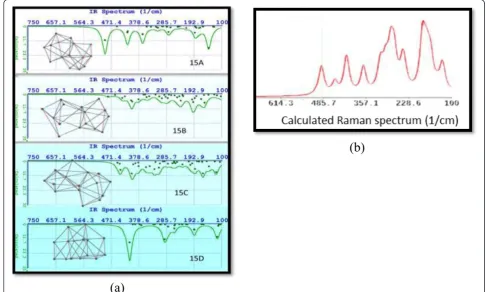
Since 1998, Ho et al. [54] employed the unbiased tight-binding model (TBM) search and disclosed the low-lying clusters 15A-15D which contain the capped trigonal prism unit form. The isomer having the global minimum at the CCSD (T)/6-31G (d) level is the 15A (C3v) one whose geometry is a tri-capped trigonal prism fused with a tri-capped trigonal anti-prism. The vibrational fre-quency analysis at the MP2/6-31G (d) level shows that the 15A isomer has two imaginary frequencies. Thus, isomer 15A (C3v) may not be a stable structure but a transition-state structure at the MP2/6-31G (d) level of theory. A structural perturbation to 15A (C3v) followed by geometry relaxation gives rise to isomer 15A with Cs symmetry (possesses only a mirror plane σh). Isomer 15A (Cs) shows no imaginary frequencies. Ours results confirm that isomer 15A has no symmetry (C1) and is the global minimum.
Figure 8a displays the molecular structures and FTIR spectra for Si15isomers. Isomers 15B and 15C show the less intensity with a scattered distribution and not well-defined peaks. There are 39 vibrational modes in these isomers.
On the other hand, isomers 15A and 15D have a var-iety of defined peaks. The most intense peak for isomer with the global minimum (15A) corresponds to a fre-quency of 493.086 cm−1, and the local minimum with the highest difference in energy (15D) displays the most intense peak at 409.9 cm−1.
We have calculated Raman spectra for all previously cited Si15isomers. Figure 8b corresponds to calculated Raman spectrum for isomer Si15A. Several models have been proposed for size calculations using Raman line shape. The model suggested by Richter, Wang, and Ley [55] (RWL) and later improved by Islam and Kumar [56] and by Mishra and Jain [57] has widely been employed. Regrettably, RWL model stands on the multiplication of the wave function in an infinite crys-tal by an arbitrary weighting functionWD(r) (Gaussian
or sine functions) in order to find the dimensions of the silicon clusters. This undiscriminating choice re-sults in quite different values at low dimension of nanocrystals [58,59].
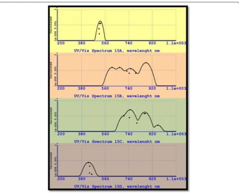
[image:10.595.53.540.420.712.2]In Figure 9, we display the UV-VIS spectra for silicon isomers from 15A to 15D. We can appreciate remark-able differences in these spectra. So, for example, the isomer 15A results with emission located at a narrow in-tense peak at 525.31 nm (green emission) and the silicon isomer 15D with a wider peak at 440.88 (blue emission).
Results obtained for isomers 15B and 15C predict emission in most of the visible region and extends until the IR region. For isomer 15B, the most intense peak lies in IR and has a wavelength of 871.74 nm, whereas for isomer 15C, the most intense peak lies at 750.42 nm (red emission).
Table 1 contains numerical data of the geometric and optical properties for isomers ranging from Si15 to Si20. For isomers Si15, the differences in the values of the en-ergies obtained with respect to isomer 15A confirm un-doubtedly the global minimum.
The band gap calculated for the most stable isomer is 3.051 eV. Also, a great value for dipole moment was ob-tained (3.097 Debye). The nano-agglomerate size of the global minimum has resulted to be the lowest of this set of isomers (0.72508 nm). Finally, the highest zero-point energy (ZPE) and ovality values correspond to the global minimum.
Structural and optical properties calculated for isomers Si16
For Si16 cluster, Zhu and Zeng [50] found that isomer 16A with C2h symmetry gives the lowest energy at the CCSD (T)/6-31G (d) level, similar to the prediction of Ho et al. [54]; nevertheless, we have found that isomer 16B is the one with the global minima with a difference of only 0.18 eV with respect to isomer 16A.
The isomer 16A can be described as two fused pen-tagonal prisms. Its structure is unique in the sense that it is neither based on the tri-capped trigonal prism motif (as 16B) nor based on a stacking sequence of fourfold and fivefold rings with capping atoms (as 16C).
[image:11.595.60.538.86.477.2]Numerical data for isomers 16A to 16C are listed in Table 1. The isomer 16B exhibits not only the lowest en-ergy and the highest band gap (2.45 eV), ovality, and ZPE but also the lowest parameter D, polarizability/ atom, and the lowest wavelength for the most intense peak, for this set of isomers.
Figure 10a displays the structure and FTIR spectra for isomers Si16. For isomer 16A, we can appreciate five peaks, two of them which are the most intense, at the frequencies of 295 and 331 cm−1. For isomer 16B, the frequencies of the two most intense peaks correspond to
[image:12.595.59.537.100.395.2]415 and 487 cm−1. In the central position of the atomic structures (left side figures) of these two isomers, we see four silicon atoms forming a cycle. On the other hand, isomer 16C is somewhat different, with only one intense peak in 345 cm−1. The 16C atomic structure does not Table 1 Structural and optical properties calculated for isomers varying from Si15to Si20
Isomer E(au) rel.E(eV) Band gap (eV) Dipole (Debye) D(nm) Polarizability/atom ZPE (eV) Ovality UV-VIS lambda max
15A −4,342.34404 0.00 3.051 3.097 0.72508 4.629 0.632 1.2115 525.314
15B −4,342.32497 0.52 1.889 0.959 0.72991 4.648 0.629 1.2035 871.635
15C −4,342.31698 0.74 1.971 0.525 0.72724 4.656 0.614 1.2099 750.415
15D −4,342.30761 0.99 3.441 0.027 0.75043 4.594 0.589 1.1645 431.109
16A −4,631.80268 0.18 1.954 0.00 0.75701 4.465 0.636 1.1833 750.886
16B −4,631.80953 0.00 2.450 0.54 0.73474 4.456 0.663 1.2189 583.651
16C −4,631.79720 0.33 2.250 0.76 0.75324 4.469 0.625 1.1911 630.165
17A −4,921.27172 0.8 1.053 2.384 0.70364 4.356 0.706 1.2540 1,033.850
17B −4,920.97362 8.659a 0.619 0.180 0.76368 4.494 0.886 1.4320 2,747.970
17C −4,921.30164 0.00 1.874 0.638 0.75456 4.311 0.757 1.2104 838.4698
18A −5,210.83526 0.00 2.255 2.84 0.74512 4.177 0.80 1.2504 552.447
18B −5,210.80158 0.92 1.388 0.04 0.73920 4.178 0.74 1.2580 692.813
18C −5,210.80010 0.96 1.323 0.01 0.73906 4.178 0.73 1.2581 1,732.74
18D Not converged
19A −5,500.25750 1.98 1.878 3.45 0.7361 4.098 0.81 1.2965 700.980
19B −5,500.33041 0.00 2.198 1.93 0.7544 4.058 0.83 1.2571 643.427
19C −5,500.28806 1.15 2.351 1.21 0.7259 4.076 0.82 1.3112 678.640
20A −5,789.84528 0.00 2.7320 1.54 0.74238 3.9476 0.92 1.3005 549.724
20B −5,789.81937 0.71 2.9045 0.00 0.75361 3.9465 0.87 1.2813 540.264
20C −5,789.76867 2.08 1.6437 0.73 0.77313 3.9727 0.90 1.2514 756.136
a
[image:12.595.59.538.486.702.2]Isomer Si17B presents and unexpected energy.
display a cycle in the middle part of the nanocrystal. In-stead of that, there are two cycles with four silicon atoms each. In all the cases, we have obtained an im-aginary frequency of vibration for isomers Si16.
Raman spectroscopy, which is a sensitive probe to the local atomic arrangements and vibrations, has been used to describe Si nanostructures [60]. The shift and half-width of the one-phonon Raman peak in c-Si have often been used to obtain an estimate of the characteristic di-mensions of the Si crystallites. We have evaluated theo-rically the Raman spectra for all Si16isomers included in this work. Particularly in Figure 10b, we show the calcu-lated Raman spectrum for isomer Si16A.
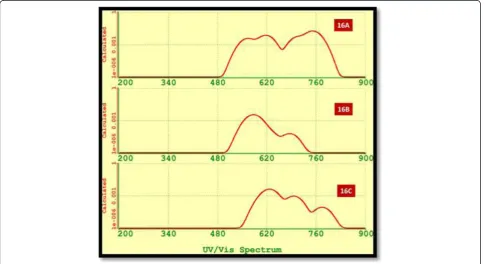
Figure 11 shows the UV-VIS spectra for isomers 16A to 16C. It is noticeable that these silicon nano-agglomerates will emit in the visible region.
For isomer 16B, the highest intensity of emission cor-responds to 583.65 nm, and the second peak observed is at a wavelength of 576 nm (both in yellow color). We observe a redshift for the other two isomers. Isomer 16B displays a wideband of emission (from green to red color), with the most intense peak at 750.89 nm (red color), while isomer 16C has the most intense calculated emission at 630.16 nm.
Structural and optical properties calculated for isomers Si17
Ho et al. [54] have reported for Si17isomers, 17A, with C3v symmetry as ‘possibly the lowest energy structure,’and it does contain a tri-capped trigonal prism (TTP) unit and a
hexagonal chair unit. The six-atom hexagonal chair unit can be viewed as a fragment in bulk diamond silicon [61,62]. The calculated emission in this work confirms this assertion (emission in the near infrared, see Table 1).
It is interesting to note that the more spherical-like Si17 isomer, 17C, is very competitive in stability com-pared to the prolate-shaped isomer 17A [59]. Using a level theory of HF/6-31G*, Zhu and Zeng [50] report isomer 17C as the structure with the global minimum in energy for Si17 isomers, and isomer 17A using other levels of theory (MP2/6-31G*, MP3/6-31G*, MP4(SDQ)/ 6-316*, CCSD/6-31G*, CCSD(T)/6-31G*). Isomer 17B exhibits an unusual energy difference of 8.659 eV with respect to the global minimum (as can be seen in Table 1). During our calculations, it had instability and troubles to get convergence. Probably, this was the rea-son for which Zhu did not report the evaluation of iso-mer 17B using other levels of theory.
The FTIR spectra for isomers Si17 are displayed in Figure 12a. Particularly, it attracts attention the fact that the isomer 17B displays calculated vibrational frequen-cies above 480 cm−1. The intensity calculated for vibra-tional frequencies for isomer 17C was very small with respect to the other two isomers Si17.
[image:13.595.57.543.452.716.2]The Raman shift due to the quantum confinement can be described by a phenomenological approach founded on the negative dispersion of optical phonons with finite mo-mentum and the averaging and folding of phonon fre-quencies in small particles. An analytic expression of this
approach to describe the Raman frequency shift as also employed by Paillard et al. [58] is Δω¼−52:3 0:543
L
1:586 ; in which 0.543 nm is the lattice constant of silicon, Lis the crystallite size, the parameter A= 52.3, and the exponent γ= 1.586 which are used to explain the vibrational
[image:14.595.59.537.89.335.2]confinement due to the finite size in a nanocrystal, and these values depend on each specific system. We have evaluated all Raman spectra corresponding to Si17isomers A to C, using DFT. Figure 12b shows, as an example, the spectrum which corresponds to isomer Si17A.
Figure 12Calculated FTIR spectra and Raman spectrum. (a)Calculated FTIR spectra for isomers from 17A to 17C. The structures of these isomers are depicted on the left side.(b)Calculated Raman spectrum for Si17A.
[image:14.595.56.540.459.714.2]Figure 13 shows the UV-VIS spectra for isomers Si17. The calculated wavelength for the emission of the most stable Si17isomer (17C) corresponds to a wideband from red to NIR (702.69 to 1,000.09 nm) with a maximum calculated intensity of 838.4698 nm.
Calculated emission for isomer 17A results in a nar-rowband with emission only in the near infrared. The predicted emission for isomer 17B is in the tail infrared but results with a very low intensity.
Structural and optical properties calculated for isomers Si18
With respect to Si18cluster, four low-lying isomers were considered, and they are shown in Figure 14. The elon-gated isomer 18A has the lowest energy at the HF/6-31G* level of theory. Isomer 18A has the structure similar to the ground-state structure of Si18+, predicted by Ho et al. [17]. It contains a magic number cluster Si6 unit and a hexagonal chair unit. A slight structural perturbation to this C3visomer followed by geometry relaxation gives iso-mer 18B with Cs symmetry. Both 18B and 18C with C2v
symmetry contain a tri-capped trigonal prism unit, and both are very viable in stability compared to 18A because the calculated difference in energy was 0.92 and 0.96 eV, respectively (see Table 1). Isomer 18D is a new isomer with high symmetry but relatively high energy. It is com-posed of two-capped tetragonal anti-prisms, and in this case, we did not obtain convergence at HF/6-31G* level of theory (see Figure 14a and Table 1).
FTIR spectra for isomer 18A shows the most intense calculated response at the vibrational frequency of 409 cm−1; nevertheless, frequencies of 450 and 458 cm−1 were calculated too.
[image:15.595.58.537.364.692.2]The shift of the phonon peak towards lower wavenum-bers and broadening of the peak width, in the Raman spectra, are attributed to the confinement of optical phonons in nano-dimensional Si crystals [63]. The shift of the phonon peak could be used to calculate the crys-tallite size of Si. Using DFT, we have evaluated the Raman spectra for isomers Si18 A to C. In Figure 14b, we display the Raman spectrum for Si18 A. In this case, the phonon peak appears at a frequency of 485.7 cm−1.
The frequencies that have been observed in experi-mental reports are a little higher than the calculated ones for this isomer (see Figure 6, left). Isomer 18B dis-plays the most intense peak at 260 cm−1. Each isomer Si18 has 48 vibrational modes. Isomer 18C presents the two most intense peaks at the vibrational frequencies 179 and 262 cm−1; and two of the calculated wavenum-ber were imaginary.
Figure 15 displays the UV-VIS calculated spectra for isomers Si18. The results obtained for these isomers pre-dict emissions in a part of the visible range, from green to red color, and IR. DFT predicts green emission due to the most intense peak for isomer 18A and in red color for isomer 18B, and the most intense peak for iso-mer 18C occurs in the IR region at 1,732.74 nm (not shown in Figure 14, refer to Table 1). For isomer 18B, additionally to emission displayed in Figure 14, we obtained a calculated emission wavelength in IR at 1,620.05 nm.
Structural and optical properties calculated for isomers Si19
Ho et al. [54] found for Si19 cluster a spherical-like iso-mer 19A. The isoiso-mer 19B which contains a tetra-capped trigonal prism unit and a magic number cluster Si6unit is very competitive in stability compared with 19A. Iso-mer 19B was found based on a novel single-parent
evolution algorithm coupled with DFTB/DFT methods. Isomer 19C is composed of a TTP unit and a Si10 (bi-capped tetrahedral anti-prism) unit [54]. Its energy is slightly higher than both 19A and 19B.
Molecular structures for three isomers Si19were calcu-lated. The nano-agglomerates Si19 are displayed on the left side of Figure 16a. The structure 19B was energetic-ally the most stable, having differences in energy with values of 1.98 and 1.15 eV with respect to silicon ag-glomerates 19A and 19C. Also, structure 19B has an intermediate value of band gap with respect to analo-gous isomers.
Figure 16a displays the FTIR spectra for isomers Si19 A, B, C. We can appreciate manifold vibrational fre-quencies varying from 200 to 500 cm−1. The strongest vibrations, for the most stable isomer, include the most intense peak at 325 cm−1, with an adjacent shoulder around 351 cm−1. The highest vibration is due to sili-con atom located in the highest part or trigonal prism. The third most important vibration of isomer 19B oc-curs at 472 and 479 cm−1and is associated to the bend-ing mode Si-Si vibration of atoms in the base of the trigonal prism.
[image:16.595.57.544.442.721.2]The atomic structure of isomer 19C seems like two small agglomerates joined, along the central part, for a simple silicon-silicon bond. The isomer 19C is the
isomer Si19 which has the smallest size and dipole mo-ment of all but presents the highest ovality (see numer-ical data in Table 1).
Raman spectroscopy provides useful information about the structure of silicon nano-agglomerates. The
[image:17.595.58.541.85.626.2]position and intensity of peaks in the spectrum reflect the molecular structure and can be used to determine the chemical identity of the sample. No two structures give exactly the same Raman spectrum, and the inten-sity of the scattered light is proportional to the amount
of material present. Raman spectroscopy has shown to be useful for investigating the physical properties such as crystallinity, phase transitions, and isomers or poly-morphs. We evaluate the Raman spectra for Si19 ag-glomerates. Figure 16b displays the Raman spectrum for Si19A.
Finally, in Figure 17, we display the UV-VIS spectrum for Si19 isomers. These three isomers resulted with cal-culated emission in the visible region. Besides, isomer 19A extends its luminescence until the near infrared. Isomer 19B which is more stable energetically has the widest band.
Conclusions
In this work, we calculated theoretically the IR, UV-VIS, and Raman spectra, the orbital energy levels including the frontier orbitals (HOMO and LUMO) and a selected set of geometric properties of medium-sized silicon ag-glomerates from Si15to Si20including all stable isomers. These Si-nCs present a size which is less than 1 nm. Their gap energies oscillate between 1.053 and 3.051 eV. The equilibrium energy calculated for several proposed Si clusters at ground state and at the first six excitation states calculated results very useful to evaluate the pos-sible impact to the PL from different silicon structures present in SRO films. From the theoretical PL spectra obtained in this work, we can conclude that this family
of silicon agglomerates emits in the visible region, ex-tending in some cases to the near infrared.
Competing interests
The authors declare that they have no competing interests.
Authors’contributions
NDET conducted the modeling of silicon nano-agglomerates and wrote the draft manuscript. DHL provided the background and support in the modeling process and corrected the draft manuscript. JFJFG provided the idea and supervised the study. JALL provided high-resolution transmission electron microscopy (HRTEM) and EFTEM studies and supervised the film growth procedures. JMJ carried out the PL and X-ray measurements in silicon samples. DEVV conducted the SiOxfilm growth. All authors read and approved the final manuscript and contributed to the analysis and discussion of results.
Authors’information
[image:18.595.58.539.90.355.2]has been working with porous materials (porous silicon and porous aluminum), their structure and electrical and optical properties. His research interests are the conduction process and the modeling of these processes. JALL is currently a researcher and professor in the Science Institute - Center of Investigation for Semiconductors Devices (IC-CIDS) of Autonomous University of Puebla, Mexico. He has been working on the structural, electrical, and optical characterization of materials and MOS structures. His research interest is the physics and technology of nanostructured materials and silicon devices. Additionally, his research interests are, too, the nanotechnology, material characterization, and optoelectronic devices such as sensor, LEDs, and solar cells. JMJ is currently a researcher and professor in the Science Institute - Center of Investigation for Semiconductors Devices (IC-CIDS) of Autonomous University of Puebla, Mexico. He has been working on compound semiconductor families III-V (GaAs, GaSb, GaAlAs, GaAlSb, GaAlSbAs, InGaSbAs), II-VI (ZnO, ZnS, CdO, CdS, CdSe, CdSSe), and IV-VI (PbS, WO3, Cu2O), epitaxial growth by LPE, synthesis by spray pyrolysis and chemical bath, semiconductor devices (LD and APDs), and structural and photoluminescence characterization of materials and devices. DEVV is currently a Ph.D. student in the Science Institute - Center of Investigation for Semiconductors Devices (IC-CIDS) of Autonomous University of Puebla, Mexico. She started to work on the growth and characterization of nonstoichiometric silicon oxide obtained by HFCVD. Her research interests include experiments and structural, optical, and electrical characterization of SiOxfilms and MOS structures.
Acknowledgements
This work has been partially supported by CONACyT-154725, PIFI-2013, and VIEP-BUAP-2013. N.D. Espinosa-Torres acknowledges the financial support of CONACYT by the scholarship given to carry out Ph.D. studies. We thank also the M.Sc. student Angel Pedro Rodríguez Victoria for his collaboration in PL measures in porous silicon.
Received: 19 May 2014 Accepted: 12 August 2014 Published: 17 September 2014
References
1. Canham LT:Silicon quantum wire array fabrication by electrochemical and chemical dissolution of wafers.Appl Phys Lett1990,57:1046–1048. http://dx.doi.org/10.1063/1.103561.
2. Amato G, Delerue C, Von Bardeleben HJ:Structural and optical properties of porous silicon nanostructures. InOptoelectronic Properties of Semiconductors and Lattices, Volume 5. Edited by Manasreh MO. The Netherlands: Gordon and Breach Science Publishers; 1997.
3. Lockwood DJ:Light emission in silicon in light emission in silicon from physics to devices. InSemiconductors and Semimetals, Volume 49. Edited by Lockwood DJ. San Diego: Academic; 1998:1–36.
4. Kanemitsu Y, Suzuki K, Kondo M, Matsumoto H:Luminescence from a cubic silicon cluster.Solid State Commun1994,89:619–621. http://www. sciencedirect.com/science/article/pii/0038109894901767.
5. Kanemitsu Y, Suzuki K, Kondo M, Kyushin S, Matsumoto H:Luminescence properties of a cubic silicon cluster octasilacubane.Phys Rev B1995,
51:10666–10670. http://journals.aps.org/prb/pdf/10.1103/PhysRevB.51.10666. 6. Furukawa K, Fujino M, Matsumoto N:Cubic silicon cluster.Appl Phys Lett
1992,60:2744–2745. http://dx.doi.org/10.1063/1.106863.
7. Yuan Z, Pucker G, Marconi A, Sgrignuoli F, Anopchenko A, Jestin Y, Ferrario L, Bellutti P, Pavesi L:Silicon nanocrystals as a photoluminescence down shifter for solar cells.Sol Energy Materials Solar Cells2011,95:1224–1227. doi:10.1016/j.solmat.2010.10.035 http://www.science.unitn.it/~semicon/ archive/2011-SEM-yuan.pdf.
8. Espinosa-Torres ND, Flores-Gracia JFJ, Luna-López JA, Hernández de la Luz D, Martínez-Juárez J:Computer simulation of luminescence in silicon rich oxide thin films arising from silicon-oxygen bonds.Int J Sci Res2014,
3(7):5–15. http://theglobaljournals.com/ijsr/file.php?val=July_2014_ 1405663706__29.pdf.
9. Espinosa-Torres ND, Gracia JFJF, López JAL, García JCR, Sánchez AM, Sánchez JLS, Hernández de la Luz D, Morales FM:Ab initio molecular orbital calculation for optical and electronic properties evaluation of small and medium size silicon nano-clusters found in silicon rich oxide films.J Mod Phys2013,4(11B):1–26. http://dx.doi.org/10.4236/
jmp.2013.411A2001.
10. Raghavachari K, Rohlfing CM:Bonding and stabilities of small silicon clusters: a theoretical study of Si7–Si10.J Chem Phys1988,89:2219–2234. http://dx.doi.org/10.1063/1.455065.
11. Luo Y, Zhao J, Wang GH:Fractional bond model for silicon clusters.Phys Rev B1999,60:10703–10706. http://dx.doi.org/10.1103/PhysRevB.60.10703. 12. Bergeron DE, Castleman AW Jr:Insights into the stability of silicon cluster
ions: reactive etching with O2.J Chem Phys2002,117:3219–3223. http://dx.doi.org/10.1063/1.1486439.
13. Yoo S, Zeng XC, Zhu X, Bai J:Possible lowest-energy geometry of silicon clusters Si21and Si25.J Am Chem Soc2003,125:13318–13319. http://dx.doi. org/10.1021/ja0365678.
14. Rohlfing CM, Raghavachari K:Structures of Si10: are there conventionally bonded low-energy isomers?Chem Phys Lett1992,198:521–525. http://dx. doi.org/10.1016/0009-2614(92)80038-D.
15. Bahel A, Ramakrishna MV:Structure of the Si12cluster.Phys Rev B1995, 51:13849–13851. http://dx.doi.org/10.1063/1.471742.
16. Zhu XL, Zeng XC, Lei YA, Pan B:Structures and stability of medium silicon clusters. II. Ab initio molecular orbital calculations of Si12–Si20.Chem Phys 2004,120:8985–8995. http://dx.doi.org/10.1063/1.1690755.
17. Ho K-M, Shvartsburg AA, Pan B, Lu Z-Y, Wang C-Z, Wacker JG, Fye JL, Jarrold MF:Structures of medium-sized silicon clusters.Nature (London)1998,
392:582–585.
18. Rata I, Shvartsburg AA, Horoi M, Frauenheim TH, Siu KWM, Jackson KA:
Single-parent evolution algorithm and the optimization of Si clusters. Phys Rev Lett2000,85:546–549. http://link.aps.org/doi/10.1103/ PhysRevLett.85.546.
19. Li BX, Cao PL, Jiang M:Twenty six stable structures for cluster Si10: a full-potential linear-muffin-tin-orbital molecular-dynamics study.Phys Status Solidi B2000,218:399–409. http://link.aps.org/doi/10.1002/1521-3951 (200004)218:2<399::AID-PSSB399>3.0.CO;2-R.
20. Guillois O, Herlin-Boime N, Reynaud C, Ledoux G, Huisken F:Photoluminescence decay dynamics of noninteracting silicon nanocrystals.J Appl Phys2004,
95:3677–3682. http://dx.doi.org/10.1063/1.1652250.
21. Aceves-Mijares M, González-Fernández AA, López-Estopier R, Luna-López A, Berman-Mendoza D, Morales A, Falcony C, Domínguez C, Murphy-Arteaga R:On the origin of light emission in silicon rich oxide obtained by low pressure chemical deposition.J Nano Mat2012,2012(890701):1–11. http://dx.doi.org/10.1155/2012/890701.
22. Efros AL, Efros AL:Fizika i Tekhnika Poluprovodnikov, vol. 16, 1982, pp 1209-1214, (in Russian), Efros, AlL, Efros AL, Engl.Transl: Sov Phys Semicond1982,16:772–776.
23. Dal Negro L, Cazzanelli M, Pavesi L, Ossicini S, Pacifici D, Franzò G, Priolo F, Iacona F:Dynamics of stimulated emission in silicon nanocrystals.Appl Phys Lett2003,82(26):4636–4638. http://dx.doi.org/10.1063/1.1586779. 24. Meldrum A, Haglund RF Jr, Boatner LA, White CW:Nanocomposite
materials formed by ion implantation.Adv Mater2001,13(19):1431–1444. http://dx.doi.org/10.1002/1521-4095(200110)13:19<1431::AID-ADMA1431>3.0. CO;2-Z.
25. Nayfeh MH, Rao S, Barry N, Therrien J, Belomoin G, Smith A, Chaieb S:
Observation of laser oscillation in aggregates of ultra-small silicon nanoparticles.Appl Phys Lett2002,80(1):121–123. http://dx.doi.org/10.1063/ 1.1428622.
26. Zacharias M, Heitmann J, Scholz R, Kahler U, Schmidt M, Bläsing J:
Size-controlled highly luminescent silicon nanocrystals: a SiO/SiO2 super-lattice approach.Appl Phys Lett2002,80(4):661–663. http://dx.doi. org/10.1063/1.1433906.
27. Xiangdong X, Shibin L, Wang Y, Fan T, Jiang Y, Huang L, He Q, Ao T:Silicon nanowires prepared by electron beam evaporation in ultrahigh vacuum. Nanoscale Res Lett2012,7(243):1–7. http://dx.doi.org/10.1186/1556-276X-7-243. 28. Gaponenko SV:Optical Properties of Semi-conductor Nanocrystals.Cambridge
University Press; 1998:245. http://dx.doi.org/10.1017/CBO9780511524141. 29. Bragg WL:The diffraction of short electromagnetic waves by a crystal.
Proc Cambridge Philos Soc1913,17:43–57. http://diamond.kist.re.kr/ knowledge/nobel-physics/1915/wl-bragg-lecture.pdf.
30. Brus LE:Electron–electron and electron–hole interactions in small semiconductor crystallites: the size dependence of the lowest excited electronic state.J Chem Phys1984,80(9):4403–4409. http://dx.doi.org/ 10.1063/1.447218.
31. Kayanuma Y:Quantum-size effects of interacting electrons and holes in semiconductor microcrystals with spherical shape.Phys Rev B1988,
32. Brus LE:On the development of bulk optical properties in small semiconductor crystallites.J Lumin1984,31:381–384. http://dx.doi.org/ 10.1016/0022-2313(84)90302-8.
33. Kayanuma Y, Momiji H:Incomplete confinement of electrons and holes in microcrystals.Phys Rev B1990,41:10261–10263http://link.aps.org/doi/ 10.1103/PhysRevB.41.10261.
34. Vatankhah C, Ebadi A:Quantum size effects on effective mass and band gap of semiconductor quantum dots.Res J Recent Sci2013,2(1):21–24. http://www.isca.in/rjrs/archive/v2i1/5.ISCA-RJRS-2012-356.pdf. 35. Kiebach R, Luna-López JA, Dias GO, Aceves-Mijares M, Swart JW:
Characterization of silicon rich oxides with tunable optical band gap on sapphire substrates by photoluminescence, UV/Vis and Raman spectroscopy.J Mex Chem Soc2008,52(3):212–218. © 2008, Sociedad Química de México ISSN 1870-249X. http://www.jmcs.org.mx/PDFS/V52/3/ 06-Characterization.pdf.
36. Laue MV:Zur dynamik der relativitätstheorie; entgegnung an Hrn: Schaposchnikow.Ann Phys1913,347:1575–1579. http://onlinelibrary.wiley. com/doi/10.1002/andp.19133471628/abstract.
37. Honea EC, Ogura A, Murray CA, Raghavachari K, Sprenger WO, Jarrold MF, Brown WL:Raman spectra of size-selected silicon clusters and comparison with calculated structures.Nature (London)1993,366:42–43. http://www. nature.com/nature/journal/v366/n6450/pdf/366042a0.pdf.
38. Santra K, Chatterjee P, Sen Gupta SP:Voigt modelling of size–strain analysis: application to a-Al2O3prepared by combustion technique. Bull Mater Sci2002,25(3):251–257. © Indian Academy of Sciences. http://link.springer.com/article/10.1007/BF02711163.
39. Warren BE, Averbach BL:The effect of cold‐work distortion on X‐ray patterns.J Appl Phys1950,21:595–598. http://dx.doi.org/10.1063/1.1699713. 40. Voyles PM, Muller DA, Grazul JL, Citrin PH, Gossmann H-JL:Atomic-scale
imaging of individual dopant atoms and clusters in highly n-type bulk Si.Nature2002,416:826–829. http://www.nature.com/nature/journal/v416/ n6883/full/416826a.html.
41. Grossman JC, Mitas L:Quantum Monte Carlo determination of electronic and structural properties of Sinclusters (n≤20).Phys Rev Lett1995, 95:1323–1326. http://link.aps.org/doi/10.1103/PhysRevLett.74.1323. 42. Luna López JA, García Salgado G, Ponce Pedraza A, Vázquez Valerdi DE,
Carrillo López J, Morales Sánchez A, Díaz Becerril T, Rosendo Andrés E, Juárez Santiesteban H:Structural and optical properties of SiOx films deposited by HFCVD.Procedia Eng2011,25:304–308. Proceedings of the Eurosensors XXV. 1877–7058 © 2011 Published by Elsevier Ltd. http://dx.doi. org/10.1016/j.proeng.2011.12.075.
43. Coyopol A, García-Salgado G, Díaz-Becerril T, Juárez H, Rosendo E, López R, Pacio M, Luna-López JA, Carrillo-López J:Optical and structural properties of silicon nanocrystals embedded in SiOx matrix obtained by HWCVD.J Nanomater2012,2012(368268):7. http://dx.doi,org/10.1155/2012/368268. 44. Pai PG, Chao SS, Takagi Y, Lucovsky G:Infrared spectroscopic study of
SiOx films produced by plasma enhanced chemical vapor deposition. Vac Sci Technol A1986,4:689–694. http://dx.doi.org/10.1116/1.573833. 45. Vásquez-A MA, Rodríguez GÁ, García-Salgado G, Romero-Paredes G,
Peña-Sierra R:FTIR and photoluminescence studies of porous silicon layers oxidized in controlled water vapor conditions.Rev Mex Fis2007,53(6):431–435. http:// www.redalyc.org/pdf/570/57053601.pdf.
46. Aceves-Mijares M, Espinosa-Torres ND, Flores-Gracia F, González-Fernández AA, López-Estopier R, Román-López S, Pedraza G, Domínguez C, Morales A, Falcony C:Composition and emission characterization and computa-tional simulation of silicon rich oxide films obtained by LPCVD.Surf Interface Anal2014,46:216–223. http://dx.doi.org/10.1002/sia.5212. 47. Pulay P:Convergence acceleration of iterative sequences: the case of
SCF iteration.Chem Phys Lett1980,73(2):393–398. http://dx.doi.org/ 10.1016%2F0009-2614%2880%2980396-4.
48. Davidson ER:The iterative calculation of a few of the lowest eigenvalues and corresponding eigenvectors of large real-symmetric matrices.J Comp Phys1975,17:87–94. http://ac.els-cdn.com/0021999175900650/1-s2.0-
0021999175900650-main.pdf?_tid=8fa52f14-44c1-11e4-93f1-00000aacb360&acdnat=1411656065_d871d1ced394e35042e008a278cfb931. 49. Møller C, Plesset MS:Note on an approximation treatment for
many-electron systems (abstract).Phys Rev1934,46(7):618–622.
Bibcode:1934PhRv…46..618M. http://link.aps.org/doi/10.1103/PhysRev.46.618. 50. Zhu X, Zeng XC:Structures and stabilities of small silicon clusters: ab
initio molecular-orbital calculations of Si7–Si11.J Chem Phys2003, 118:3558–3570. http://dx.doi.org/10.1063/1.1535906.
51. Scuseria GE, Schaefer HF III:Is coupled cluster singles and doubles (CCSD) more computationally intensive than quadratic configuration-interaction (QCISD)?J Chem Phys1989,90:3700–3703. http://dx.doi.org/10.1063/1.455827. 52. ŘezáčJ,Šimová L, Hobza P:CCSD[T] describes noncovalent interactions better
than the CCSD(T), CCSD(TQ), and CCSDT methods.J Chem Theory Comput
2013,9(1):364–369. http://pubs.acs.org/doi/abs/10.1021%2Fct3008777. 53. Rassolov VA, Pople JA, Ratner MA, Windus TL:6-31G* basis set for atoms K
through Zn.J Chem Phys1998,109(4):1223–1229.
54. Liu B, Lu Z-Y, Pan B, Wang C-Z, Ho K-M, Shvartsburg AA, Jarrold MF:
Ionization of medium-sized silicon clusters and the geometries of the cations. J Chem Phys1998,109:9401–9409. http://dx.doi.org/10.1063/1.477601. 55. Richter H, Wang ZP, Ley L:The one phonon Raman spectrum in microcrystalline silicon.Solid State Common1981,39:625–629. 56. Islam MN, Kumar S:Influence of crystallite size distribution on the
micro-Raman analysis of porous Si.Appl Phys Lett2001,78:715–717. http://dx.doi.org/10.1063/1.1343494.
57. Mishra P, Jain KP:Raman, photoluminescence and optical absorption studies on nanocrystalline silicon.MaterSci Eng B2002,95:202–213. http://www.sciencedirect.com/science/article/pii/S0921510702002349. 58. Paillard V, Puech P, Laguna MA, Charles R, Kohn B, Huisken F:Improved
one-phonon confinement model for an accurate size determination of silicon nanocrystals.J Appl Phys1999,86:1921–1924. http://dx.doi.org/ 10.1063/1.370988.
59. Zi J, Buscher H, Falter C, Lugwig W, Zhang K, Xie X:Raman shifts in silicon nanocrystals.Appl Phys Lett1996,69:200–202. http://dx.doi.org/10.1063/ 1.117371.
60. Furukawa S, Miyasato T:Quantum size effects on the optical band gap of microcrystalline Si:H.Phys Rev B1988,38(8):5726–5729. http://link.aps.org/ doi/10.1103/PhysRevB.38.5726.
61. Tomanek D, Schluter MA:Calculation of magic numbers and the stability of small Si clusters.Phys Rev Lett1986,56:1055–1058. http://link.aps.org/ doi/10.1103/PhysRevLett.56.1055.
62. Tomanek D, Schluter MA:Structure and bonding of small semiconductor clusters.Phys Rev B1987,36:1208–1217. http://link.aps.org/doi/10.1103/ PhysRevB.36.1208.
63. Sui Z, Leong PP, Herman IP, Higashi GS, Temkin H:Raman analysis of light-emitting porous silicon.Appl Phys Lett1992,60(17):2086–2088. http://dx. doi.org/10.1063/1.107097.
doi:10.1186/1556-276X-9-507
Cite this article as:Espinosa-Torreset al.:Evaluation of optical and electronic properties of silicon nano-agglomerates embedded in SRO: applying density functional theory.Nanoscale Research Letters
20149:507.
Submit your manuscript to a
journal and benefi t from:
7Convenient online submission
7Rigorous peer review
7Immediate publication on acceptance
7Open access: articles freely available online
7High visibility within the fi eld
7Retaining the copyright to your article