N A N O E X P R E S S
Open Access
High-resolution X-ray diffraction analysis of strain
distribution in GaN nanowires on Si(111) substrate
Hryhorii Stanchu
1, Vasyl Kladko
1, Andrian V Kuchuk
1,2*, Nadiia Safriuk
1, Alexander Belyaev
1, Aleksandra Wierzbicka
3,
Marta Sobanska
3, Kamil Klosek
3and Zbigniew R Zytkiewicz
3Abstract
In this work, the influence of micro- and macro-deformation profiles in GaN nanowires (NWs) on the angular intensity distribution of X-ray diffraction are studied theoretically. The calculations are performed by using kinematical theory of X-ray diffraction and assuming the deformation decays exponentially from the NW/substrate interface. Theoretical modeling of X-ray scattering from NWs with different deformation profiles are carried out. We show that the shape of the (002) 2θ/ωX-ray diffraction profile (XDP) is defined by initial deformation at the NW's bottom and its relaxation depth given by the decay depth of the exponential deformation profile. Also, we demonstrate that macro-deformation leads to XDP shift, whereas micro-deformations are the cause of XDP's asymmetry and its symmetrical broadening. A good correlation between calculated and experimental XDP from self-assembled GaN NWs on Si(111) substrate was achieved by taking into account all parameters of micro- and macro-deformation profiles.
Keywords:Nanowires; GaN; Deformation; X-ray diffraction profile; Kinematical theory
Background
The wide range of unique properties of semiconductor GaN nanowires (NWs), along with various techniques of NW's growth, makes them promising candidates for nano-sized optoelectronics [1]. In recent years, a great deal of effort has been devoted to explore their optical, electrical, and structural properties. The main sources of deterioration of NW's properties are their crystalline imperfection and residual strain. Generally, NWs are considered almost strain-free crystalline-objects with-out extended defects that propagate into their structure [2-5]. In comparison with thick planar epilayers, where the mechanism of lattice accommodation is preferably plastic and where the formation of misfit dislocation networks takes place, NWs are considered to be pre-dominantly free of dislocations [6,7]. At the same time, the process of deformation relaxation in NWs is not completely studied.
Over recent years, there have been only a few significant reports devoted to this subject. In [2], the assessment of
macro- and micro-deformation in GaN NWs grown on Si(111) was performed with X-ray diffraction, where the NWs were found to be free of deformations on the macro scale but not on the micro scale. In comparison to self-assembled GaN NWs [2], an exponential relaxation of the macro-strain along the NW height was observed for top-down fabricated GaN NWs grown on silicon and sapphire substrates [3,4]. An exponential decay of the mean-squared micro-strain along the self-assembled GaN NW was considered to describe the X-ray diffraction peaks in [8]. Moreover, theoretical analysis of the elastic energy relaxation in NWs of different geometries grown on lattice mismatched substrates was performed assuming an exponential decay of strain [9].
In this letter, we study the influence of macro- and micro-deformation along the GaN NW's growth axis on the X-ray diffraction peak profile. We show that macro-deformations lead to X-ray diffraction profile (XDP) shift, whereas micro-deformations are the cause of XDP's asymmetry and its symmetrical broadening. This allows distinguishing the influence of macro- and micro-deformation components on XDP and thereby to extract them separately.
* Correspondence:[email protected] 1
V. Lashkaryov Institute of Semiconductor Physics, National Academy of Sciences of Ukraine, Pr. Nauky 45, Kyiv 03028, Ukraine
2
Institute for Nanoscience and Engineering, University of Arkansas, W. Dickson731, 72701 Fayetteville, AR, USA
Full list of author information is available at the end of the article
Methods
Self-induced GaN NWs were grown by plasma-assisted molecular beam epitaxy (MBE) on a Si(111) substrate at approximately 760°C under highly nitrogen-rich con-ditions. Before the growth started, the substrate was exposed to a nitrogen flux for 30 min at the nitridation temperature of approximately 150°C. The procedure of plasma-assisted MBE growth of GaN NWs on Si(111) is described in [10,11]. The high-resolution X-ray diffraction measurements were performed by using PANalytical X'Pert Pro MRD diffractometer (PANalytical, Almelo, the Netherlands) equipped with a 1.6 kW X-ray tube (vertical line focus) with CuKα1radiation (λ= 1.540598 Å), a
sym-metric 4 × Ge(220) monochromator and a channel-cut Ge (220) analyzer.
Results and discussion
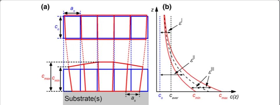
A large jump of deformation occurs at the GaN/substrate interface, due to the large mismatch of the lattice parame-ters and coefficients of thermal expansion between GaN and conventional substrates. As GaN NWs are bounded by free surfaces, the misfit deformation that is mainly con-centrated at the NW/substrate heterointerface elastically relaxes to the NW's free sides. Therefore, the deformation of a whole NW and at the heterointerface will consider-ably differ, i.e., deformation decreases from the bottom to the top of NW, as schematically shown in Figure 1.
Depending on the crystal's considering volume, defor-mations are divided into two groups: macro-deformation (ε|) and micro-deformations (ε|| and ε|||). The macro-deformation ε| is an integral deformation of a whole sample. On the other hand, deformationsε||andε|||occur in a limited part of a crystal and lattice unit volume, respectively. We consider that NWs are mostly deformed
at their bottoms, thus they can be assumed to be free ofε|. As it is shown in Figure 1b, for a particular height of NW, we define ε||(z) as the average lattice cells deformation along the NW diameter (see Equation 1), while ε|||(z) is the deformation fluctuation around the
ε||
(z) (see Equation 2):
εjjð Þ ¼z cmaxð Þ þz cminð Þz
2co −
1; ð1Þ
εjjjð Þ ¼z cmaxð Þz−co
co −ε
jjð Þ ¼z εjjð Þz−cminð Þz−co
co ; ð
2Þ
withco=0.51851 nm - bulk GaN lattice parameter; cmin
(z) and cmax(z) are the minimal and maximal deviation
from co of the out-of-plane lattice parameter along the
GaN nanowire's diameter at NW's heightz.
The deformation profiles of ε||(z) andε|||(z) along the NW's growth axis are defined assuming exponential de-formation decay [3,4,8,9]:
εj jjj j= z
ð Þ ¼εj jjj j=
o e
−z
LR; ð3Þ
whereLRis the deformation relaxation depth, at which the
deformation relaxes to1/eof the initial values (εjjo or εjojj),
andzis the NW's height.
[image:2.595.57.539.513.694.2]A simple simulation of XDP was performed to get infor-mation about the deforinfor-mation distribution in GaN NWs. Here, we simulated a symmetric (002) 2θ/ω diffraction profile using the kinematical theory of X-ray diffraction. The deviations of the out-of-plane lattice parameter from the bulk value along the NW's height appear as variations in the length of the scattering vector q at which the Bragg's condition is satisfied. According to the geometry conditions of the scattering process for symmetric reflec-tions [12], the length of q=kin−kout (where kin and kout
are the incident and scattered wave vectors, respectively) is related to the incidence angleθby:
q¼qz ¼2j jk sinð Þθ : ð4Þ
Taking into account the Bragg's law 2d(00l)sin(θ) =nλ,
we can present the length of the scattering vector pro-portional to the lattice parameterc(z):
qðh¼k¼0Þ¼ nl
c zð Þ; ð5Þ
where (hkl) are Miller indices and n is the diffraction order.
Thus, from Equations 4 and 5, one can see that the change in the lattice parameterc(z) along the NW height is the origin of intensity distribution in Equation 6, where the intensity was obtained by summing amplitudes reflected by each crystal plane:
I qð Þ ¼ X N
i
Fiexpð−2πiq zð iþu zð ÞÞÞ
2
; ð6Þ
whereFiis the structure factor of a plane at depthzi;N
is the number of crystal planes and u(z) =〈u(z)〉±δu(z). Here,〈u(z)〉=ε||(z)⋅coandδu(z) =ε|||(z)⋅coare the
devi-ations of NW's lattice parameterc(z) from the bulk value
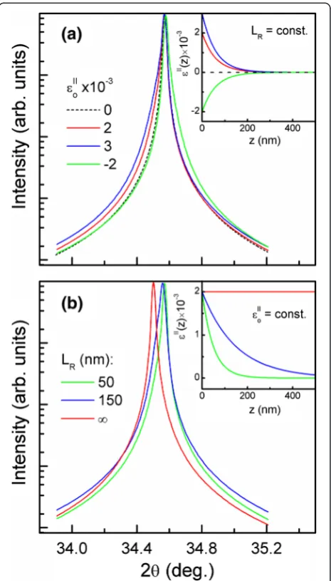
co, caused by deformationsε||(z) andε|||(z), respectively. Different types of deformation lead to specific changes in the XDP. In Figure 2, we demonstrate a calculated (002) 2θ/ω XDP for a 500-nm-long GaN NWs array affected only by micro-deformationε||(z). We show how the magnitude of initial deformation εjjo (caused by the
lattice misfit at the NW/substrate interface) and the deformation relaxation depth LR (dependent on the
aspect ratio of NW) contribute to the XDP. It is shown (Figure 2a) that forLR= const, the increase of magnitude
of micro-deformation at the NW/substrate interface
εjjo leads to asymmetrical XDP broadening, whereas the
deformation sign (tensile or compressive deformation) defines the broadening direction. Similarly (Figure 2b), for εjjo¼const; we demonstrate that the magnitude of
deformation relaxation depth (LR) is another source of
asymmetrical XDP broadening. Moreover, when LR
exceed some critical value (for a specific aspect ratio of NW), which leads to the XDP shift, we can conclude on the presence of macro-deformation ε|. Thus, the value of this deformation can be estimated directly from the magnitude of the XDP shift. It should be noted that the asymmetric broadening and shift of XDP for GaN NWs was observed experimentally in [3,4].
Next, we analyze the influence of only micro-deformationε|||(z) (caused by the elastic strain relaxation at the free NW's surface) on the XDP's shape. According
to the definition, this unsigned deformationε|||(z) is the deformation fluctuation around the ε||(z), and it is described by the same law (see Equation 3). Thus, for
LR= const and εjjo¼0; we calculated (002) 2θ/ω XDP
[image:3.595.306.539.88.496.2]for a 500-nm-long GaN NWs array affected only by micro-deformation ε|||(z). It is shown (Figure 3) that the increase of ε|||(z) magnitude leads only to symmetrical XDP broadening. It should be noted that coalescence of NWs and lattice distortion have a strong influence on deformation profile of ε|||(z) [8,13]. Actually, all kinds of deformations are not independent, and a nonlinear change of ε|||(z) deformation leads to an appearance of ε||(z)
Figure 2The calculated (002) 2θ/ωXDPs for GaN NWs.
(a)The influence of the deformation magnitude (εjjo) at the NW/ substrate interface.(b)The influence of the deformation relaxation depth (LR). The insets show the deformation profiles (defined by
deformation. Moreover, the increase of micro-deformation (ε||(z)) relaxation depth LR leads to the appearance of a
macro-deformation (ε|). Thus, to fit the theoretical XDP from GaN NWs to the experimental one, the distribution of micro- and macro-deformation profiles should be taken into account.
Then, we consider the simulation of XDP from self-induced GaN NWs grown on Si(111) substrate. In order to evaluate the macro- and micro-deformation state of GaN NWs, we first used a standard approach based on measurements of reciprocal space map (RSM) and a series of symmetrical (00 l) 2θ/ω reflections (l =2,4,6). From the angular position of GaN(105) and Si(224) peaks on RSM (Figure 4), we conclude on almost fully relaxed state of GaN NWs on the macro scale (R = (Δθexp/Δθbulk)⋅100 %≈99 %). Here,ΔθexpandΔθbulkare
the differences between angular positions of GaN(105) and Si(224) peaks measured experimentally and their bulk values, respectively. On the other hand, the hetero-geneous micro-deformation along the NWs c-axis and a small vertical correlation length (VCL) contribute to the broadening of the symmetrical 2θ/ω reflections in radial scan direction. These two effects have different depend-encies on the diffraction vector and can be separated using Williamson-Hall (WH) plots [14,15]. The WH plot analysis (inset in Figure 4) gives the value of VCL equal to approximately 285 nm and the average micro-deformation approximately 0.53 × 10⁻⁴.
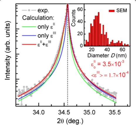
Further, we calculated the XDP for a whole GaN nano-wire ensemble taking into account the NW diameter distribution. We used the approach presented in [8],
where the XDP of each NW is multiplied byD2(whereD
[image:4.595.307.540.88.315.2]is the NW's diameter) and the frequency of the corre-sponding nanowire diameter. Experimental and calculated (002) 2θ/ωXDPs of GaN NWs are shown in Figure 5. The simulated XDP (red line) is plotted along with the XDPs where either the ε|||(z) or ε||(z) is taken into account individually (blue and green line, respectively). It is demonstrated that in order to achieve a good Figure 3The calculated (002) 2θ/ωXDPs for GaN NWs affected
[image:4.595.57.292.88.304.2]by the micro-deformationεIII(z).The deformation distribution profiles ofεIII(z) used for XDP calculation were defined by Equation 3 and are shown in the inset.
Figure 4The asymmetrical reciprocal space maps near the Si(224) and GaN(105) reflections.The inset presents the Williamson-Hall plot for the symmetrical (00 l) GaN reflections (l= 2,4,6).
[image:4.595.306.538.472.685.2]fitting of experimental 2θ/ωXDPs, both components of micro-deformation should be considered. Moreover, since no peak shift is observed, we conclude that the NWs are free of macro-deformation ε|, which well correlates with results obtained from RSM. The large asymmetry of the red XDP indicates significant ε||(z) tensile micro-deformation at the bottom of the GaN NWs. The calcula-tion provides the value of deformacalcula-tion relaxacalcula-tion depthLR
to be 1.4 times larger than the NW's diameter and the magnitude ofε||(z) of the order of 10−3, which are close to values obtained in [3,4,8]. Also, the fitting procedure gives the average NW's heightzequal to 400 nm, which corre-lates well with values obtained from cross-sectional SEM image (not shown here). The average value of micro-deformation <ε|||(z) > ~ 1.7 × 10⁻⁴is in good agreement with the values presented in [2,13] for GaN NWs grown also on Si(111). Thus, in comparison with standard WH analysis based on FWHM of 2θ/ω-scans (which gives the average value of VCL and micro-strain fluctuation), the calculation of the full XDP allows to evaluate the macro-and micro-deformation depth profiles macro-and more accurate value of the NW's height.
Conclusions
In this work, the theoretical analysis of micro- and macro-deformation parameters that influence symmetrical (002) 2θ/ω XDP from GaN NWs is presented. It is demon-strated that the macro-deformation ε| of a whole NW leads to the angular position shift of XDP. Inhomogeneous micro-deformation ε||(z) along the NW height leads to asymmetry of the XDP. The micro-deformation ε|||(z) fluctuation around the ε||(z) causes only broadening of XDP. Thus, our theoretical approach of 2θ/ωXDP calcu-lation can be used for quantitative analysis of GaN NWs with different shapes and deformation states.
Competing interests
The authors declare that they have no competing interests.
Authors’contributions
AK and HS designed and drafted the manuscript. AW and NS performed XRD measurements. MS and KK grew the structures. VK, AB, and ZRZ coordinated the study. All authors read and approved the final manuscript.
Acknowledgements
This study was supported by the National Academy of Sciences of Ukraine within the framework of the scientific-technological program‘Nanotechnology and Nanomaterials’2010 to 2014, project no. 3.5.1.12/19.
Author details
1
V. Lashkaryov Institute of Semiconductor Physics, National Academy of Sciences of Ukraine, Pr. Nauky 45, Kyiv 03028, Ukraine.2Institute for
Nanoscience and Engineering, University of Arkansas, W. Dickson731, 72701 Fayetteville, AR, USA.3Institute of Physics, Polish Academy of Sciences, Al.
Lotnikow 32/46, 02-668 Warsaw, Poland.
Received: 22 October 2014 Accepted: 19 January 2015
References
1. Consonni V, Feuillet G. Self-induced growth of GaN nanowires by molecular beam epitaxy. In: Consonni V, Feuillet G, editors. Wide band gap semiconductor nanowires for optical devices: low-dimensionality related effects and growth. NJ: John Wiley & Sons, Inc; 2014. p. 177–215. 2. Jenichen B, Brandt O, Pfuller C, Dogan P, Knelangen M, Trampert A.
Macro- and micro-strain in GaN nanowires on Si(111). Nanotechnology. 2011;22:295714.
3. Hugues M, Shields P, Sacconi F, Mexis M, Auf der Maur M, Cooke M. Strain evolution in GaN nanowires: from free-surface objects to coalesced templates. J Appl Phys. 2013;114:084307.
4. Tseng W, Gonzalez M, Dillemans L, Cheng K, Jiang S, Vereecken P. Strain relaxation in GaN nanopillars. Appl Phys Lett. 2012;101:253102.
5. Thillosen N, Sebald K, Hardtdegen H, Meijers R, Calarco R, Montanari S. The state of strain in single GaN nanocolumns as derived from micro-photoluminescence measurements. Nano Lett. 2006;6:704–8. 6. Shumin W. Heterostructures and strain relaxation in semiconductor
nanowires. In: Shumin W, editor. Lattice engineering: technology and applications. Singapore: Pan Stanford; 2013. p. 189–229.
7. Haab A, Mikulics M, Sutter E, Jin J, Stoica T, Kardynal B. Evolution and characteristics of GaN nanowires produced via maskless reactive ion etching. Nanotechnology. 2014;25:255301.
8. Kaganer V, Jenichen B, Brandt O, Fernandez-Garrido S, Dogan P, Geelhaar L. Inhomogeneous strain in GaN nanowires determined from x-ray diffraction peak profiles. Phys Rev B. 2012;86:115325.
9. Zhang X, Dubrovskii V, Sibirev N, Ren X. Analytical study of elastic relaxation and plastic deformation in nanostructures on lattice mismatched substrates. Cryst Growth Des. 2011;11:5441–8.
10. Wierzbicka A, Zytkiewicz Z, Kret S, Borysiuk J, Dluzewski P, Sobanska M. Influence of substrate nitridation temperature on epitaxial alignment of GaN nanowires to Si(111) substrate. Nanotechnology. 2013;24:035703.
11. Borysiuk J, Zytkiewicz Z, Sobanska M, Wierzbicka A, Klosek K, Korona K. Growth by molecular beam epitaxy and properties of inclined GaN nanowires on Si(001) substrate. Nanotechnology. 2014;25:135610. 12. Kuchuk A, Stanchu H, Chen L, Ware M, Mazur Y, Kladko V. Measuring the depth
profiles of strain/composition in AlGaN-graded layer by high-resolution x-ray diffraction. J Appl Phys. 2014;116:224302.
13. Fernández-Garrido S, Kaganer V, Hauswald C, Jenichen B, Ramsteiner M, Consonni V. Correlation between the structural and optical properties of spontaneously formed GaN nanowires: a quantitative evaluation of the impact of nanowire coalescence. Nanotechnology. 2014;25:455702. 14. Metzger T, Hopler R, Born E, Ambacher O, Stutzmann M, Stommer R. Defect
structure of epitaxial GaN films determined by transmission electron microscopy and triple-axis X-ray diffractometry. Philos Mag A. 1998;77:1013–25. 15. Kladko V, Kuchuk A, Stanchu H, Safriuk N, Belyaev A, Wierzbicka A.
Modelling of X-ray diffraction curves for GaN nanowires on Si (111). J Cryst Growth. 2014;401:347–50.
Submit your manuscript to a
journal and benefi t from:
7 Convenient online submission
7 Rigorous peer review
7 Immediate publication on acceptance
7 Open access: articles freely available online
7 High visibility within the fi eld
7 Retaining the copyright to your article