ABSTRACT
KONG, XIANGCHENG. Predictive Modeling and Optimization for Vibration-assisted AFM Tip-based Nanomachining. (Under the direction of Prof. Jingyan Dong and Prof. Paul H. Cohen)
The tip-based vibration-assisted nanomachining process offers a low-cost, low-effort
technique in fabricating nanometer scale 2D/3D structures in sub-100 nm regime. To understand its mechanism, as well as provide the guidelines for process planning and
optimization, we have systematically studied this nanomachining technique in this work. To understand the mechanism of this nanomachining technique, we firstly analyzed the interaction between the AFM tip and the workpiece surface during the machining process. A
3D voxel-based numerical algorithm has been developed to calculate the material removal rate as well as the contact area between the AFM tip and the workpiece surface. As a critical
factor to understand the mechanism of this nanomachining process, the cutting force has been analyzed and modeled. A semi-empirical model has been proposed by correlating the cutting force with the material removal rate, which was validated using experimental data from
different machining conditions. With the understanding of its mechanism, we have developed guidelines for process planning of this nanomachining technique. To provide the guideline
for parameter selection, the effect of machining parameters on the feature dimensions (depth and width) has been analyzed. Based on ANOVA test results, the feature width is only controlled by the XY vibration amplitude, while the feature depth is affected by several
machining parameters such as setpoint force and feed rate. A semi-empirical model was first proposed to predict the machined feature depth under given machining condition. Then, to
machining parameters could be provided using these predictive feature dimension models. As
the tip wear is unavoidable during the machining process, the machining precision will gradually decrease. To maintain the machining quality, the guideline for when to change the tip should be provided. In this study, we have developed several metrics to detect tip wear,
such as tip radius and the pull-off force. The effect of machining parameters on the tip wear rate has been studied using these metrics, and the machining distance before a tip must be
Predictive Modeling and Optimization of Vibration-assisted AFM Tip-based Nanomachining
by
Xiangcheng Kong
A dissertation submitted to the Graduate Faculty of North Carolina State University
in partial fulfillment of the requirements for the degree of
Doctor of Philosophy
Industrial Engineering
Raleigh, North Carolina 2017
APPROVED BY:
_______________________________ _______________________________
Jingyan Dong Paul H. Cohen
Co-Chair of Advisory Committee Co-Chair of Advisory Committee
_______________________________ _______________________________
DEDICATION
BIOGRAPHY
Xiangcheng Kong received B.S. degree in Physics from Shandong University in 2013. Since August 2013, he joined Prof. Jingyan Dong and Prof. Paul H. Cohen’s group in Edward P.
Fitts Department of Industrial and Systems Engineering at North Carolina State University.
ACKNOWLEDGMENTS
I’d like to express my deepest gratitude to my advisors, Dr. Jingyan Dong and Dr. Paul H.
Cohen, for providing me such a great opportunity to work with them. I also would like to thank the rest of my committee, Dr. Yong Zhu, Dr. Rohan Shirwaiker for their valuable
suggestions and feedback. Finally, I would like to thank Dr. Gracious Ngaile for taking the role of Graduate School Representative for my final defense.
It has been my great pleasure to work with the most talented and motivated colleagues, Dr. Li Zhang, Dr. Chuang Wei, Jia Deng, Yiwei Han, Dr. Hantan Qin, Dr. Zhuo Tan, Yi Cai,
Hengfeng Gu, Arun Kumar and Pedro Huebner. Your friendship and support makes my life
TABLE OF CONTENTS
LIST OF TABLES ... viii
LIST OF FIGURES ... ix
CHAPTER 1 INTRODUCTION ... 1
1.1 Background ... 1
1.2 Motivation ... 2
1.3 Research hypotheses ... 3
1.4 Outline ... 4
CHAPTER 2 LITERATURE REVIEW ... 6
2.1 AFM-based nanofabrication methods ... 6
2.1.1 Dip-pen lithography ... 6
2.1.2 Anodic oxidation lithography ... 7
2.1.3 Mechanical direct scratching ... 8
2.1.4 Dynamic plowing lithography ... 9
2.1.5 Ultrasonic force microscopy ... 10
2.1.6 Rotating tip based nanomilling ... 11
2.2 Cutting force modeling ... 12
2.3 Tool wear models ... 19
2.4 Chapter Summary ... 24
CHAPTER 3 VIBRATION-ASSISTED TIP-BASED PLATFORM ... 25
3.2 Vibration-assisted nanomachining process ... 26
3.3 Analysis of the experimental platform ... 28
CHAPTER 4 PREDICTIVE MODELING FOR FEATURE DIMENSIONS ... 32
4.1 Experimental design ... 32
4.2 Analysis of feature width ... 33
4.3 Analysis of feature depth ... 34
4.4 Predictive models for feature dimensions ... 37
4.4.1 (a) Estimation of the contact area between the tip and sample surface ... 38
4.4.1 (b) Development of semi-empirical model for feature depth prediction ... 43
4.4.2 Regression models for feature depth prediction ... 47
4.5 Model validation and comparison ... 49
4.6 Chapter summary ... 51
CHAPTER 5 PREDICTIVE CUTTING FORCE MODEL ... 52
5.1 Numerical model to calculate material removal rate ... 53
5.2 Predictive modeling for feature dimensions ... 56
5.3 Dynamic cutting force modeling in nanomachining process ... 58
5.4 Chapter Summary ... 66
CHAPTER 6 Modeling of tip wear ... 68
6.1 Tool wear during machining process ... 68
6.2 Tip wear measurement through SEM images ... 69
6.3 Tip wear detection through pull-off force ... 72
6.5 The effect of machining parameters on tip wear ... 81
6.6 Modeling the tip change frequency ... 87
6.7 Chapter summary ... 91
CHAPTER 7 OPTIMIZATION MODELS FOR UNIT PRODUCTION TIME AND COST ... 93
7.1 Process modeling in conventional scale ... 93
7.2 Process planning for vibration-assisted tip-based nanomachining ... 94
7.3 Stop criterion to change the tip ... 96
7.4 Process optimization for minimum production time ... 101
7.5 Process optimization to minimize production cost ... 105
7.6 A case study for process planning and optimization ... 108
7.7 Chapter Summary ... 110
CHAPTER 8 CONCLUSION ... 112
8.1 Summary ... 112
8.2 Future work ... 114
8.2.1 Real-time process monitoring ... 115
8.2.2 Process simulation ... 115
8.2.3 Process optimization for machining 3D patterns ... 116
REFERENCES ... 117
APPENDIX ... 126
Appendix A ... 127
LIST OF TABLES
Table 4.1 A full factorial design experiment with three factors ... 33
Table 4.2 Significance test for feature width (x1: setpoint force, x2: XY vibration amplitude, x3: Feed rate) ... 34
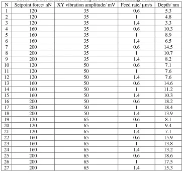
Table 4.3 Measured feature depth for all machining conditions ... 35
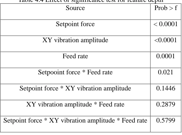
Table 4.4 Effect of significance test for feature depth ... 37
Table 4.5 The root mean square of relative errors for all of three predictive models ... 50
Table 5.1 Machining tests for force modeling with the predicted and measured feature depth and width by predictive feature dimension models ... 58
Table 6.1 Parallel study to analyze the tip wear during machining process ... 70
Table 6.2 Factorial design experiments (23) for tip wear study. ... 77
Table 6.3 The average rate of change of pull-off forces (nN/pattern) during the first five patterns under different machining conditions. After we can see, with larger setpoint force or feed rate, the average rate of change of pull-off forces are also larger. ... 80
Table 6.4 The machined distance (µm) when cross-point occurred ... 87
Table 6.5 The estimated cut-off pull-off forces based on experience ... 89
Table 6.6 The number of machined patterns calculated using both cross-point method and cut-off pull-off force method. ... 90
Table 7.1 The tip life calculated using transition point ... 97
Table 7.2 The calibrated coefficients for Equation 7.7 ... 99
Table 7.3 The calibrated coefficients for Equation 7.10 ... 100
Table 7.4 The designed feature dimensions and single tip changing time ... 109
Table B.1 Measured Pull-off forces (nN) under 500 nN, 1 μm/s. ... 155
Table B.2 Measured Pull-off forces (nN) under 500 nN, 2 μm/s. ... 155
Table B.3 Measured Pull-off forces (nN) under 500 nN, 3 μm/s. ... 155
Table B.4 Measured Pull-off forces (nN) under 1000 nN, 1 μm/s ... 156
Table B.5 Measured Pull-off forces (nN) under 1000 nN, 2 μm/s ... 156
Table B.6 Measured Pull-off forces (nN) under 1000 nN, 3 μm/s ... 156
Table B.7 Measured Pull-off forces (nN) under 1500 nN, 1 μm/s ... 157
Table B.8 Measured Pull-off forces (nN) under 1500 nN, 2 μm/s ... 157
Table B.9 Measured Pull-off forces (nN) under 1500 nN, 3 μm/s ... 158
Table B.10 Measured average feature depth (nm) under 500 nN, 1 μm/s ... 158
Table B.11 Measured average feature depth (nm) under 500 nN, 2 μm/s ... 159
Table B.12 Measured average feature depth (nm) under 500 nN, 3 μm/s ... 159
Table B.13 Measured average feature depth (nm) under 1000 nN, 1 μm/s ... 159
Table B.14 Measured average feature depth (nm) under 1000 nN, 2 μm/s ... 159
Table B.14 Continued ... 159
Table B.15 Measured average feature depth (nm) under 1000 nN, 3 μm/s ... 159
Table B.16 Measured average feature depth (nm) under 1500 nN, 1 μm/s ... 160
Table B.17 Measured average feature depth (nm) under 1500 nN, 2 μm/s ... 160
LIST OF FIGURES
Figure 3.1 Schematic illustration ... 27
Figure 3.2 Virtual tool illustration. The tip is vibrated in an in-plane circular path. ... 27
Figure 3.3 Top view of the engagement between virtual tool and sample ... 28
Figure 3.4 Schematic illustration of experimental setup ... 29
Figure 4.1 The relationship between feature width and XY vibration amplitude (35, 50, 65 mV separately). We can observe a strong linear correlation between width and XY vibration amplitude... 34
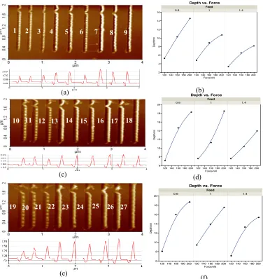
Figure 4.2 Experiments results. (a) (c) (e) show feature machined with different setpoint force and feed rate under 35 mV, 50 mV and 65 mV XY vibration amplitude separately. (b) (d) (f) show the relationship between feature depth and setpoint force under different feed rate with 35 mV, 50 mV and 60 mV XY amplitude separately. These experimental results demonstrated that all machining parameters like setpoint force, XY vibration amplitude and feed rate will affect feature depth. With larger setpoint force and larger XY vibration amplitude, we can get larger feature depth, while with larger feed rate, the feature depth will decrease. ... 36
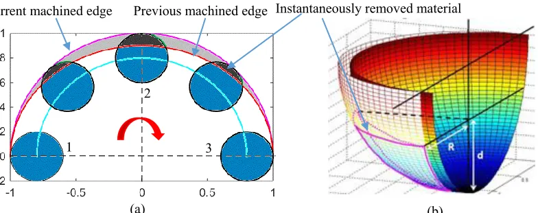
Figure 4.3 (a) Top-view of AFM tip movement and tip-sample engagement in one machining circle. (b) 3D view of the interaction area. The deep grey area in (a) are the instantaneously removed area at current tip position, which are shown as 3D view the area enclosed by the pink lines in figure (b)... 39
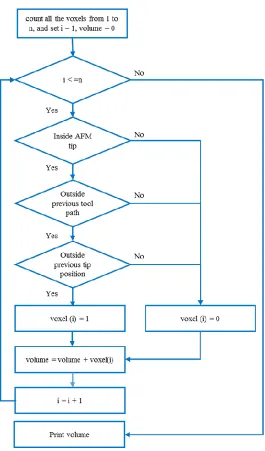
Figure 4.4. A voxel matrix of AFM tip embedded in sample. The overlapped volume between the tip and sample indicates the removed material by AFM tip. (b-e) Steps to estimate the instant removed material. (b) shows all the voxels at current tip position. (c) The voxels inside AFM tip. (d) The voxels inside AFM tip minus the region from outside of previous tool path. (e) the voxels from (d) minus of region from the outside of previous tip position, which is material removed at current location. ... 41
Figure 4.5 The instantaneous contact area (The blue area corresponding to the contact area between AFM tip and sample surface). The blue area is discretized into voxels and its area can be calculated by counting the number of voxels. ... 42
Figure 4.6. (a) The measured depth (blue) and predicted depth (red) of the semi-empirical model for experiments from Table 4.3. (b) The relative error of the model prediction. ... 46
Figure 4.7 (a) The measured depth (blue) and predicted depth (red) of the linear model for experiments from Table 3. (b) The relative error of the model prediction. ... 48
Figure 4.8. (a) The measured depth (blue) and predicted depth (red) of the nonlinear model for experiments from Table 3. (b) The relative error of the model prediction. ... 49
Figure 4.9 (a) The measured depth (blue) and predicted depth (red) of the semi-empirical model for experiments from Table 3. (b) The relative error of the model prediction. ... 50
Figure 5.1 Numerical algorithm to estimate the volume of instantaneously removed material. ... 55
Figure 5.2 (a) View of removed material at different tip angle. (b) The calculated material removal rate during one machining cycle. ... 56
Figure 5.4 (a) calculated material removal rate during machining cycles. (b) Predicted and measured lateral force. (c) Predicted and measured normal force ... 62 Figure 5.5 Comparison of (a) predicted and measured lateral force (b) predicted and
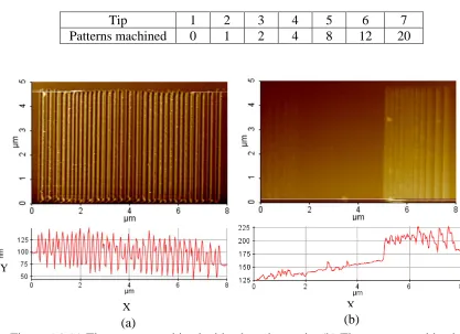
measured normal force for experimental conditions 1-9 in Table 5.1. ... 63 Figure 5.6 The machined slots for the machining conditions 10-16 in Table 1 with different feed rates. ... 65 Figure 5.7 Comparison of (a) predicted and measured lateral force. (b) predict and measured machining power. ... 65 Figure 5.8 Lateral force from the machining force model and measured lateral force for all the conditions from table 5.1. ... 66 Figure 6.1 (a) The pattern machined with a brand-new tip, (b) The pattern machined with a worn tip. As we can see, with a brand-new tip, the pattern quality is very high, and the machined feature depth is around 25 nm. However, using a worn tip, only some of the
designed trenches was machined, and the machined feature depth is much smaller. ... 70 Figure 6.2 SEM images for tip 1 to tip 7. As we can see, the tip is very sharp before
machining, however, with more patterns machined, the tip became blunter, and the tip radius became larger. ... 71 Figure 6.3 (a) The measured feature depth during machining process, (b) the measured tip radius during machining process. As we can see, with a new tip, the machined feature depth is around 23 nm. However, with more patterns machined, the machined feature depth gradually decreased. After 15 patterns, the machined feature depth was zero (no patterns could be observed). During this process, the tip radius gradually increased from 0 to 208 nm. ... 72 Figure 6.4 Force-distance curve obtained from AFM “Indentation mode”. The X axis
represents the displacement of the cantilever, and the Y axis represents the normal force applied on the cantilever. The red line represents the retraction curve, while the blue curve represents the approach curve. The force is measured by deflection of the AFM cantilever and the pull-off force is defined as the maximum attraction force during retraction of the tip for silicon surface. ... 74 Figure 6.6 Both the measured tip radius and pull-off force are plotted. As shown in the figure, with more patterns machined, both the tip radius and pull-off force increased. Also, the pull-off force is strong correlated with the tip radius, the rate of these two variables are close, which indicates the pull-off force could be employed to detect tip wear. ... 75 Figure 6.7 Machined patterns machined by Tip 7 at different tip wear stages when the
Figure 6.10 The values of measured feature depth versus the number of patterns machined. As we can see, with more patterns machined, the feature depth decreases, and the rates of change of pull-off forces are different at different tip wear stages. ... 81 Figure 6.11 Plot of both measured feature depth and pull-off forces. The blue dots represent the machined feature depth, while the boxes represent the pull-off forces. Based on the rate of change of pull-off forces or feature depth, the tip wear process can be identified as three regions: Initial tip wear region, transition region and tip failure region. ... 83 Figure 6.12 The response surface of the slopes of the local fitting lines. As we can see, the slope increases with larger setpoint force or feed rate. Also, under the same machining condition, the slope during the tip failure region is obviously larger than the one during the initial tip wear region. ... 84 Figure 6.13 The plot of both global fitting line and local fitting line for (a) initial tip wear region and (b) tip failure region when the setpoint force and feed rate were set as 1000 nN and 2 µm/s. The blue dots represent the measured pull-off forces, the green lines represent the global fitting lines and the red lines represent the local fitting lines. As we can see, the green lines are very close to the red ones, which indicates the global fitting lines are close to the local fitting lines... 86 Figure 6.14 Plot of both transition points. The boxes are the measured pull-off forces, the red line and green line are the global fitting lines for the initial tip wear region and tip failure region separately. The yellow dot and blue dot represent the transition point and cut-off point separately. As we can see, these two points are very close, which indicates the predicted results from these two models are close. ... 91 Figure 7.1 The framework of process planning. We have developed different models to provide guidelines for machining parameter selection, process monitoring and tip wear analysis. ... 96 Figure 7.2 Estimate tip life using the measured feature depth. The blue dots represent the machined feature depth; the yellow line represents the linear regression line fitted for
Figure 7.7 The response surface of optimal feed rate under different stop criterions and tip price. As we can see, the optimal feed rate increases with smaller tip price or larger stop
criterions. ... 108
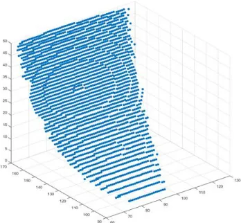
Figure A.1 Patterns machined by Tip 2. Tip 2 has been applied to machined 1 pattern, with 32 trenches. ... 127
Figure A.2 Patterns machined by Tip 3. Tip 3 has been applied to machined 2 patterns, and each pattern has 32 trenches. ... 127
Figure A.3 Patterns machined by Tip 4. Tip 4 has been applied to machined 4 patterns, and each pattern has 32 trenches. ... 128
Figure A.4 Patterns machined by Tip 5. Tip 5 has been applied to machined 8 patterns, and each pattern has 32 trenches. ... 129
Figure A.5 Patterns machined by Tip 6. Tip 6 has been applied to machined 12 patterns, and each pattern has 32 trenches. ... 130
Figure A.5 Continued... 131
Figure A.6 Patterns machined by Tip 8 under 500 nN, 1 μm/s condition. ... 132
Figure A.7 Patterns machined by Tip 9 under 500 nN, 2 μm/s condition. ... 132
Figure A.8 Patterns machined by Tip 10 under 500 nN, 3 μm/s condition. ... 133
Figure A.9 Patterns machined by Tip 11 under 1000 nN, 1 μm/s condition. ... 134
Figure A.10 Patterns machined by Tip 12 under 1000 nN, 3 μm/s condition. ... 135
Figure A.11 Patterns machined by Tip 13 under 1500 nN, 1 μm/s condition. ... 136
Figure A.12 Patterns machined by Tip 14 under 1500 nN, 2 μm/s condition. ... 137
Figure A.13 Patterns machined by Tip 15 under 1500 nN, 3 μm/s condition. ... 138
Figure A.14 Measured pull-off forces during machining process under different machining conditions. The measured pull-off increases with more patterns machined. However, the rates of change of pull-off forces are larger with larger setpoint force or feed rate. ... 139
Figure A.14 Continued... 140
Figure A.14 Continued... 141
Figure A.15 Measured feature depth during machining process under different machining conditions. With more patterns machined, the measured depth decreased, which indicates the tip became blunter. However, the values of decrease rate are different machining conditions. ... 142
Figure A.15 Continued... 143
Figure A.15 Continued... 144
Figure A.16 Different tip wear regions during machining process. The yellow lines divide the tip wear process into three different regions, including 1. The initial tip wear region, which occurs during the first few patterns. 2. The transition region, which is the region when the machined feature depth rapidly decreased, the pull-off force quickly increased. 3. Tip failure region, which is the region when the tip could not machine patterns under the given machining condition. As we can see, with larger setpoint force, more patterns were machined during the initial tip wear region, which indicates larger setpoint force could raise the limit of maximum patterns could be machined of the AFM tip. ... 145
CHAPTER 1 INTRODUCTION
1.1 Background
Nanotechnologies have been widely applied in many areas such as physics, chemistry, biological science, and engineering. To achieve these applications,
nanofabrication techniques especially fabrication of master patterns and masks are critical. Many nanofabrication methods have been developed previously, such as X-ray lithography [1], e-beam lithography [2, 3], nanoimprint lithography [4], etc. Although these methods can
achieve nanometer scale resolution, many of them still rely on e-beam lithography to fabricate the mold or mask, which is costly. Atomic Force Microscope (AFM) based
nanomachining provides a low-cost, easy-to-setup alternative to the above-mentioned nanolithography methods.
The traditional tip-based nanomachining approach can directly modify the sample by
plastic deformation with low-cost, while the major disadvantage of this method is its low efficiency. As the machined feature dimensions are mainly controlled by the AFM tip radius, multiple times of scratching are needed to make a relatively large feature. Moreover, poor
controllability is another disadvantage of this method. Usually a large normal force is required to push the AFM tip into the workpiece surface and achieve desired feature depth
[5]. Thus, the tip will wear out quickly. Previous researchers have demonstrated that by adding XY high frequency vibration, the feature width can be fully controlled. Also, the normal force and the tip wear can be greatly reduced [6].
cutting forces between the cutting tool and the workpiece surface, 2) providing a guideline
for parameters selection, and 3) modeling of tool wear. [7-10] However, for machining in nanometer scale, the machining conditions are significantly different than those in conventional scale. For example, the dimensions of machined features in nanometer scale are
close to the dimensions of the cutting tool. Moreover, for our vibration-assisted tip-based nanomachining process, the machining process involves many complex machining scenarios,
such as rotary motion and partial engagement between the tip and the workpiece surface, so it is very difficult to understand the mechanism of material removal. There is little research on the understanding of nanomachining process, hence the importance of systematically
analyzing and modeling the process.
1.2 Motivation
This vibration-assisted tip-based nanomachining process has been successfully applied to machine 2D or 3D patterns previously, and the machined patterns show good machining accuracy and surface finish [11].However, the selection of machining parameters
is usually based on operators’ experience, which may not be adequate for designed features and the role of machining forces is not well understood. Also, commercialization of this
nanomachining technique will require potential users to effective apply the process through guidelines for process planning and answer the following questions:
1. As in conventional scale machining, it is critical to know what are the feasible
machining parameters to achieve desired feature depth and width. In this vibration-assisted tip-based nanomachining process, three machining parameters
amplitude and the feed rate, so we need to understand the effects of these three
machining parameters on the feature depth and width.
2. During this nanomachining process the AFM tip may become damaged (e.g. wear or fracture), which will greatly impact the machining accuracy and production
efficiency. To avoid these issues and maintain the machining quality, we must monitor the machining process in real-time using the cutting forces, which could
be obtained using the signal feedback system. However, to employ the cutting forces to monitor the machining process, we must understand the effects of machining conditions on the cutting forces, and can calculate the cutting forces
under different machining conditions
3. It is critical to provide the guideline for when to change the tip, because if we
change the tip too frequently, the production cost will be high. However, if we fail to change the tip on time, the machining accuracy will be greatly affected and the surface finish will be bad.
4. For this tip-based nanomachining, based on our experience, the unit production cost is very high. Also, as the machining speed is µm/s scale, the total production
time is long if we need to machine thousands of patterns. Thus, it is critical to optimize the machining process by minimize the production cost and maximize the production efficiency.
1.3 Research hypotheses
such as setpoint force, the XY vibration amplitude, and feed rate. Second, cutting forces
during the machining process are proportional to the instantaneous material removal rate. Third, the tip wear is significantly affected by several factors, such as the machining distance, setpoint force, and feed rate. Finally, the production time and production cost are
affected by machining parameters, such as setpoint force and feed rate, which can be optimized to achieve minimum production time or cost.
1.4 Outline
In Chapter 2, the current research advances in the tip-based nanomachining area is introduced, as well as modeling methods to predict interaction force and tip wear. In Chapter
3, the experimental platform used in this research is described. In Chapter 4, the interaction between the AFM tip and workpiece surface will be discussed; a numerical model will be
proposed to estimate the contact area between these two. Then, a semi-empirical model will be proposed and validated to predict the feature dimensions under given machining parameters. Also, regression models are also developed as alternatives. The performance of
these models will be discussed. In Chapter 5, to calculate the interaction forces between the tip and workpiece surface, a semi-empirical model is proposed by correlating the forces with
material removal rate. Due to the difficulties of analytically calculating the material removal rate, the numerical model used in Chapter 4 is modified to calculate the volume of instantaneously removed material during machining cycle as well as material removal rate.
To investigate different machining conditions, we conduct a factorial design experiment. The feature dimensions of machined patterns using each machining condition are predicted and
proposed semi-empirical model is calibrated using the predicted feature dimensions and
calculated material removal rate. Chapter 6 discusses tip wear during machining process. Several metrics are explored to detect tip wear including tip radius and pull-off force between the tip and workpiece surface. Then, to study the effects of machining conditions on tip wear,
a factorial design experiment is conducted, and the tip wear is compared. In Chapter 7, process optimization models and their constraints are discussed. By solving these
CHAPTER 2 LITERATURE REVIEW
In this chapter, we will first introduce some of the commonly used AFM-based
nanofabrication methods, such as dip-pen lithography, anodic oxidation lithography. Then, we will review some cutting force models for both conventional scale machining and
nanoscale machining. Finally, we will introduce some tool wear models developed previously.
2.1 AFM-based nanofabrication methods
2.1.1 Dip-pen lithography
Dip-pen lithography nanolithography (DPN) is a nanofabrication technology that
atomic force microscope (AFM) tip is used to create patterns on a substrate surface with a variety of inks [12]. This technology allows surface patterning with a resolution of 100 nm scale. DPN method has been applied to fabricate nanostructures with both organic and
inorganic materials. One important application is to use an AFM tip to deliver molecules to a solid substrate via capillary transport. Hong et al. reported that DPN could be applied to pattern monolayers of different organic molecules, with nanometer scale separation [13].
Ki-Bum Lee et al. reported using DPN to construct protein arrays with feature dimensions between 100 to 350 nm [14]. For inorganic materials, such as metals, oxides, and magnetic
compounds, the feasibility of DPN method has also been investigated. Carno et al. developed two methods to precisely position gold nanoparticles on SAM-covered Au substrate. And they found that the 3D positions of the nanoparticles could be precisely controlled by AFM,
2.1.2 Anodic oxidation lithography
Anodic AFM-based nanolithography has been heavily studied previously. For this fabrication method, a bias voltage is applied between the AFM tip and the workpiece surface, which usually ranges from 108 to 1010 V/m. With this bias voltage, the geometry, as well as the electro-physical properties of the workpiece surface, will be modified. The mechanism of this lithography method is that due to the humidity of the air, both the AFM tip and the
workpiece surface are covered with a very thin water film. A water bridge will be formed if the distance between AFM tip and the workpiece surface is small enough, which is the result of the capillary effect. After applying a strong electronic field, the tip and the workpiece
surface will behave like anode and cathode separately and the area right beneath AFM tip on the workpiece surface will be oxidized. AFM anodic oxidation method can be employed to
fabricate oxide structures on semiconductors, metal etc. This method was first demonstrated by M. Yasutake et al. [16]. The AFM tip was applied with a negative voltage with respect to the silicon substrate. H. C. Day et al. applied AFM with a conductive tip to perform localized
oxidation of silicon, the fabricated lines dimensions are within 100 nm [17]. P.M. Campbell et al. applied this oxidation method to fabricate nanometer scale side-gated silicon field effect
transistors (FET) [18]. E. S. Snow et al. created a mask with linewidth around 10 nm by integrating anodic oxidation lithography with electron cyclotron resonance (ECR) source dry etching method [19]. H.T. Soh et al. used this method to fabricate a metal oxide
semiconductor field effect transistor (MOSFET) on silicon with channel length in sub-100 nm scale [20]. Besides semiconductors, AFM anodic oxidation can also be applied to metals.
on Ti films [21]. The width of the wires and resistance of the junctions are controlled in real
time. This method has also been applied to fabricate atomic point contacts on thin Al films.
2.1.3 Mechanical direct scratching
Due to its low cost and easy to setup properties, the AFM tip-based mechanical direct
scratching method has been heavily studied in recent years. To modify the workpiece surface, a large normal force is applied to the AFM tip to push it into the workpiece surface.
One advantage of this method is no subsequent transfer processes needed. Additionally, the final structure can be fabricated at one time; Usually, the workpiece surface is imaged before machining, and then after setup, the AFM tip is applied to scratch one line or multiple lines.
After machining, the workpiece surface will be imaged again to obtain the patterns machined. As this tip-based direct scratching method only involves mechanical interaction
between AFM tip and the workpiece surface, it can be applied to machine patterns on the surface of different substrate materials like polymer films, metals, etc. M. Malekian et al. applied retrofitted commercial AFM to study the cutting behavior on nanometer scale
chromium workpiece [22]. T. Sumomogi et al. investigated the applications of direct mechanical scratching method by applying very sharp diamond AFM tips to scratch on pure
metal surfaces including Ni, Cu, and Au [23]. X. Li et al. used this method to scratch the surface of the single gold nanowire to fabricate nano slot and nanopatterns [24]. Te-Hua Fang et al. simulated the nano scratching process on Au and Pt films with molecular dynamic
(MD) simulation method. In the simulation, the effect of applied load, hold time, and machining temperature was analyzed, these results were also compared with experimental
AFM tip-based direct scratching method has also been reported to be applied to
fabricate nanostructures on polymethylmethacrylate (PMMA) surface. S. Yamamoto et al. first fabricated the patterns on the ultra-thin PMMA film, then transferred the machined patterns to SiO2 substrate by wet etching. The patterns fabricated on SiO2 have a width less than 28 nm and depths of 10 nm [26]. This direct scratching nanolithography has been reported to be applied to fabricate patterns on polymers and monolayers.
Although this direct scratching approach has many advantages, such as easy to setup and low cost, a large normal force is usually needed to push the AFM tip into the workpiece surface, which results in a large friction, fast tip wear, and reduced tip life. Also, as the
engagement between the tip and the workpiece surface is difficult to control, the interaction forces between these two can be very large, which will limit the machining speed. In recent
years, many investigations have been conducted to overcome these disadvantages, improve the controllability and machining speed of this tip-based direct scratching process. Y. Yan et al. integrated a commercial AFM system with a precision stage, which is similar to
conventional CNC machining system [5]. Diamond tips are employed as the cutting tool to scratch on the workpiece surface, and both 2D and 3D microscale and nanoscale structures
were fabricated. Then, they further improved this fabrication method by applying close-loop control in this system for 3D machining, such as 3D portrait of human face, nanoline arrays of sine-wave and triangular nanostructures.
2.1.4 Dynamic plowing lithography
Dynamic plowing lithography (DPL) is another commonly used AFM tip-based
AFM tapping mode. With the assistance of the applied vibration, the controllability has been
greatly improved.
AFM-based DPL method was first introduced by B. Klehn et al. They applied a vibrating AFM tip to indent on a photoresist layer [27], and transferred the machined patterns
to SiO2 layer by wet chemical etching. Then, they further transferred the patterns from SiO2 layer to the Si substrate using KOH etching. With this method, 60 nm wide V-shape grooves
were machined. M. Heyde et al. modified the PMMA surface using plastically indenting. They have verified that the workpiece surface can be either imaged or modified by changing the vibration amplitude of the cantilever or the indentation depth [28]. B. Cappella et al.
studied the mechanism of DPL and polymeric debris formation process by analyzing the nanoindentation process with DPL method on PMMA and polystyrene (PS) films [29, 30].
They reported the stiffness and hardness of polymers can be modified by dynamic plowing method: Surrounding the fabricated patterns, the border walls or debris were created, whose dimensions were larger than the dimensions of the structures fabricated. The result indicated
that the polymer entity was loosened after fast indentation of the AFM tip.
2.1.5 Ultrasonic force microscopy
In traditional machining, ultrasonic vibration has been widely used to reduce friction in many machining processes [31]. In nanoscale, the ultrasonic vibration has also been introduced to some AFM-based imaging method, such as ultrasonic force microscopy
(UFM). The UFM is a microscope designed for nanoscale topographical and elasticity measurements for stiff materials which are difficult to analyze by traditional AFM. The
occurs in the acoustic microscope. An image with much more details than the topography can
be generated by analyzing the elastic changes. This ultrasonic force microscope was first proposed by O. Kolosov et al. to detect ultrasonic vibration of the workpiece surface in AFM using nonlinearity in the tip-workpiece interaction force curve F(z) [32]. It was discovered
that after the amplitude of AFM cantilever exceeded a threshold value, a strong repulsive force would be observed, which is caused by the nonlinearity in the tip-workpiece
interaction. Also, an AFM cantilever could detect ultrasonic vibration with frequencies up to the MHz range. K. Yamanaka et al. successfully imaged subsurface with nanometer scale resolution using UFM and analyzed the subsurface images, as well as the effect of contact
elasticity in UFM, were analyzed [33]. The mechanism of UFM can be explained as follows: when a sample is vibrated at a frequency which is much higher the resonant frequency of the
AFM tip, the tip will be frozen and indent into the sample surface. By modulating the amplitude of ultrasonic vibration, the subsurface images have been acquired by the cantilever deflection. O. Kolosov et al. applied UFM to study the structure of strained Ge islands grown
on a Si substrate [34]. By integrating the sensitivity of acoustic microscopy with a nanoscale resolution of atomic force microscopy. The local surface elasticity variations between Ge
dots and the substrate were imaged with UFM, with a spatial resolution of around 5 nm. F. Dinelli et al. have demonstrated the capability of UFM to image surface elastic properties of stiff materials [35], the UFM was applied to image heterogeneous nanostructures with a
lateral resolution of nanometers.
2.1.6 Rotating tip based nanomilling
parameters can potential affect the shape and regularity of fabricated patterns, such as
material properties (hardness and stiffness), the AFM tip geometry, and some machining parameters (setpoint force, machining speed).
To overcome the drawbacks mentioned above, such as low material removal rate and
low throughput, a rotating tip based nanomachining method has been developed by B. A. Gozen et al., which was named nanomilling [36, 37]. For this nanomachining method, the
AFM tip is integrated with a three-axis piezoelectric actuator, which provides high-speed rotary movement. With this high precision nanopositioning stage, the machining depth and width become controllable, so the desired pattern can be machined in a single path, which
means the production efficiency and product accuracy will be improved. The authors have demonstrated the nanomachining process has the capability of regulating feature dimensions
on SU-8 polymeric film. They also studied in details about the design and evaluation of a mechanical system for the nanomilling process.
2.2 Cutting force modeling
For conventional scale machining, many investigations have been conducted to understand the machining mechanism and model the machining processes. The purpose of
these investigations can be summarized into three categories: 1) optimizing machining conditions to achieve minimum production cost or production time, 2) selection of a feasible cutting tool and 3) selection of feasible coolant/lubricant. Different types of models have
Some models focus on the understanding of these mechanical variables, such as
stresses, strains and machining temperature. Some are built to predict the process performance, such as tool wear and production time.
Mechanical models have been widely used to predict some machining parameters,
such as the cutting forces, and temperature. Zhongtao Fu et al. proposed an analytical method to model the milling force in helical end milling process based on a predictive machining
theory [38]. This model has many input variables such as material properties of the workpiece, the cutting tool geometry, the cutting conditions and the milling type. In their model, the cutting edges are discretized into infinitesimal elements along the cutter axis, and
the cutting force applied to each element was predicted analytically. Then, the cutting forces were calculated by integrating all the forces along the cutter axis. The model was verified
using data from previous publications. A. Moufki et al. applied predictive machining theory to study the peripheral milling process [39]. This predictive machining theory was proposed based on an analytical thermomechanical approach of oblique cutting. Some material
characteristics, such as strain rate sensitivity, strain hardening and thermal softening, are considered. Umut Karagüzel et al. developed a process model for turn-milling operations
[40]. In their research, the uncut chip geometry and tool-work engagement limits for orthogonal, tangential and co-axial turning-milling operations were defined. Then, a novel analytical turn-milling force model was developed, which was verified by experimental data.
For some machining processes, due to their complicated machining mechanism, it is very difficult to model using mechanical methods. So, numerical modeling methods like
based on the modified Bai-Wierzbicki material model [41]. The model was validated using
data from longitudinal turning experiments conducted on AISI 1045 steel. They also investigated the longitudinal turning process using different cutting tools and process conditions. A high-speed camera was used to record the chip formation and chip flow
process, which was compared with the simulation results. T. Özel et al. investigated the turning process of Ti-6Al-4V titanium alloy and IN100 nickel-based alloy with uncoated and
TiAIN coated tools [42]. They built 3D finite element (FE) model to predict the turning forces as well as the induced stress fields. The predicted stress fields were compared with measured residual stresses. W.B. Lee et al. investigated the shear angle prediction and cutting
force variation induced by crystallographic anisotropy [43]. To consider the effect of different crystallographic orientations on the cutting process, they implemented the
constitutive equation of crystal plasticity by the finite element modeling of the chip formation at micro-scale. Two distinguished phases of pre-compression and steady-state cutting was revealed. The predicted patterns of cutting force variation agreed with published
experimental results. Yao Xi et al. investigated the improvement in machinability during thermally assisted turning of the Ti-6Al-4V alloy with finite element modeling [44]. They
developed a 2D thermally assisted model, and then validated this model by comparing the simulation data with experimental ones. The effect of workpiece temperature on the cutting force and chip formation process was analyzed. V. Vijayaraghavan et al. introduced a
combined finite element based data analytics model. The finite element model was developed to predict the cutting forces while genetic programming method was used to obtain the
using diamond tools, M. Salahshoor et al. developed a finite element simulation model of
orthogonal cutting without explicit chip formation using the plowing depth approach [46]. In recent years, some fuzzy methods like artificial intelligence (AI) haven been proposed to predict cutting forces during machining processes. Djordje Cica et al.
investigated the prediction of parameters in turning using soft computing techniques [47]. The experimental research focused on the effect of different methods of cooling and
lubricating of the cutting zone, such as the conventional method of cooling and lubricating with high-pressure jet-assisted machining, minimal quantity lubrication technique. To predict the cutting force, they created two different models, namely, artificial neural network and
adaptive networks based fuzzy inference systems. Ali R. Yildiz developed an optimization approach based on artificial bee colony algorithm to search for the optimal cutting
parameters in the turning operations [48]. Different evolutionary-based optimization techniques were also compared by the author to solve multi-pass turning optimization problems.
D. J. Waldrof et al. compared several models on the flow of workpiece material around the edge of an orthogonal cutting tool [49]. M. Fontaine et al. analyzed the effect of
tool-surface inclination on cutting force for ball-end milling [50]. The study also studied the effect of different cutting conditions, such as plowing and inclination angle, on the cutting forces by building a predictive milling force model.
Like traditional machining, it is critical to estimate the cutting forces for the micro/nanomachining process. K.S Woon et al. investigated the effect of tool edge radius on
model [52]. M. Malekian et al. built models to study the machining factors that may affect
micro-milling forces, which including plowing, elastic recovery, run-out and dynamics [53]. M.P. Vogler et al. analyzed the surface generation process in the micro-end milling for both single phase and multiphase sample materials [54]. To predict the effects of the cutter edge
radius on the cutting forces, they also proposed a model by correlating the cutting force with the minimum chip thickness concept.
As the AFM-based nanofabrication methods can easily achieve nanometer-scale resolution, they have been used widely in recent years. Like conventional scale machining, it is crucial to understand their machining mechanism and model the cutting forces during the
machining process. However, due to the complexity of these AFM-based nanomachining processes, such as nanometer scale resolution as well as partial indentation of the AFM tip,
the above-mentioned modeling methods for conventional machining are not feasible. To analyze and model the nanofabrication processes, some approaches have been proposed, such as molecular dynamics (MD) method. The MD method was developed to study
nanomachining processes by simulating the interaction between AFM tip and the workpiece surface, which can be applied to study the cutting forces, stress state, and machining energy.
The diamond tool wear was modeled by K. Cheng et al. using MD simulation method. Its basic mechanism was revealed as the thermos-chemical wear [55]. X.S. Han et al. applied MD method to study the effect of tool angles and tool edge radii for the nanometric cutting
process on single crystal silicon [56]. M.B. Cai et al. used MD approach to simulate the nanoscale ductile mode cutting of monocrystalline silicon wafer [57].
Besides the MD simulation method, the interaction forces between the AFM tip and the
workpiece surface can also be obtained by analyzing the feedback signal collected by the photodetector. Many investigations have been conducted using this method; L. Li et al. quantitatively studied the frictional properties of self-assembled alkanethiol monolayers on
Au by analyzing the friction forces recorded by the photodetector [58]. Y. Yan et al. measured 3D force components after applying B. Bhushan’s calibration method and verified
the method by friction coefficient measurement between the diamond tip and sample (sapphire) surface [59]. They claimed that the proposed method can be applied in the measurement of cutting forces in AFM tip-based nanomachining.
As the machining parameters may greatly affect the AFM-based nanomachining processes, many papers can be found in this area. The effects of some machining parameters,
such as normal force, scratch directions, are discussed. S. C. Minne et al. studied the effects of the AFM tip geometry and scratching direction on the scratched patterns [60]. A pyramidal diamond coated Silicon tip was selected to scratch on the Ni80Fe20 coated Silicon substrate in four different directions. The Ni80Fe20 thin film was deposited on the Si substrate by an e-beam deposition process, so the film is nearly isotropic. During the machining
process, a constant normal force is applied to the AFM tip. The results indicated that the direction of scratching had a significant effect on the machined feature dimensions. Tseng et al. have studied the relationship between the scratch force and the grooves’ dimensions
(depth and width) for different materials like Si, Ni, and Ni80Fe20 [61]. The scratch force applied varies from 1 to 9 µN, and a logarithmic relationship has been built to describe the
d F( n)1Ln F F( n t1) 2.1
2 2
( ) ( )
f n n t
w F Ln F F 2.2
where α1 and α2 are the scratch parameters defined as the scratch penetration depth and penetration width; Ft1 and Ft2 are the threshold forces based on the feature dimensions. The parameter of α is a measure of the machining efficiency of the tip to a specific material, the
threshold force Ft can be considered as the minimum normal force to scratch a measurable groove. These two equations have been verified by experimental data from several types of metals. As mentioned above, the parameter α is defined as d/Ln(Fn/Ft), which is the ratio of the depth of the groove to the logarithm of the normalized cutting force. Based on the definition, the ratio α can be viewed as a measure of the scratch efficiency of the tip to a
specific material, which means, with higher α value, the machined groove depth can be larger
on given material. The threshold force Ft can also be used to determine the machinability. With larger threshold, it will be more difficult to machine on this material, and larger normal
force is needed to scratch a measurable groove. Tseng et al. defined a ratio, α/Ft, called scratch ratio (SR), to represent the scratch behavior. Similar to conventional machining processes, the SR should be considered as a material property used to quantify the
machinability.
As mentioned above, the threshold force reflects the difficulties of machining on the
surface of a specific material. To provide guidelines for the selection of applied force during scratching process, it’s important to investigate the theoretical value of threshold force based
on material properties. Per the definition of threshold force, no starch occurs if the substrate
threshold force, the relationship between the contact area Ac and the normal contact force Fc, can be expressed as Equation 2.3:
(3 )2 3
4 c c c c F R A C E
2.3
Where R is the radius of the tip, and Ec is the contact elastic modulus, which is defined as Equation 2.4:
2 2
1 1
1 t s
c t s
v v
E E E
2.4
Where E is Young’s modulus; v is Poisson’s ratio, t and s corresponding to the material
property of the tip and substrate. Cc is a contact constant and equal to 2π based on JKR theory [62].
Tseng et al. then correlated the contact force with Ec, the hardness of the substrate H, the tip radius R. Then they compared the results calculated based on this model with the
results from previous experiments [63-65]. The accuracy of this model for predicting the threshold force has been validated with a wide range of materials.
2.3 Tool wear models
For conventional tool wear, many analysis and modeling methods have been developed including numerical simulation, finite element analysis, and empirical modeling
techniques. These modeling methods have been applied to different machining processes like turning, milling and cutting processes. Analytical models have been developed to describe
cutting power model in face milling operation [66]. The cutting conditions and average tool
flank wear during milling process were considered in this model. This cutting power model was employed to calculate the normal cutting power for tool wear monitoring. M.S. Kasim et al. investigated the tool wear for a ball-type end mill [67]. The tool life and wear mechanism
for machining Inconel 718 were examined using a physical vapor deposition (PVD) coated carbide tool under different cutting conditions. As the pitting was responsible for notching
and flaking, they developed a mathematical model to predict the location of these pitting. Then the location calculated could be employed to estimate the location associated with the maximum load occurred during the cutting process. The results from the predictive model
were very close to actual notching/flaking locations. K.D. Bouzakis et al. created a predictive model for the wear of the milling parts with complicated geometry [68]. The model
correlated the tool wear evolution in milling process with other factors on the cutting edge entry impact duration, and the parameters of this model were determined based on experimental results. With this model, the expected tool wear evolution can be estimated
during the numerically controlled milling process. F. Köppl et al. developed an empirical tool wear prognosis model to improve the predictability of the maintenance stops [69]. Based on
the new Soil Abrasivity Index (SAI), this model could estimate the distance between maintenance stops and the required amount of cutting tools to be changed. The prognosis model was validated based on the original reference projects.
Due to the difficulties to build analytical models, numerical methods have also been adapted to predict the tool wear during machining processes. Jerzy Rojek et al. presented a
thermomechanical algorithm was implemented in a discrete element program and used to
simulate the rock cutting with a single pick of a dredge cutter head. B. Haddag et al. used a multi-steps modeling strategy based on several numerical calculations [71]. The first step was using 3D thermomechanical analysis for the chip formation process. Some machining
outputs like cutting forces, chip morphology chip flows direction and tool-chip interface parameters were obtained. The second step was to predict the tool wear using tool-chip
interface parameters. Finally, a 3D thermal analysis of the heat diffusion was conducted by adequate thermal loading. The data obtained at each step were compared with experimental results. M. Kolahdoozan et al. investigated and optimized the tool wear in drilling process of
difficult-to-cut nickel-based superalloy [72]. Mathematical models were deduced by Minitab software to display the effect of the main cutting variables including cutting speed, feed rate
and tool diameter on tool wear. Based on finite element method (FEM), a wear process model of twist drill was built, which provided a novel approach to study the mechanism of drill wear. It was demonstrated that the simulated data matched with experimental data. To
study the effect of microstructural changes and the cooling/lubrication effects during the cutting process, Giovanna Rotella et al. developed an FE model for describing the
microstructural changes during dry and cryogenic cutting of Ti6Al4V [73]. The model was validated with experimental data. Yung-chang Yen et al. applied finite element method (FEM) to predict the tool wear evolution and tool life in the orthogonal cutting process [74].
In their model, they proposed three different parts. Firstly, they developed a tool wear model for the specified tool. Then, they modified the commercial FEM code to allow tool wear
in metal cutting operations [75]. They adopted simulation strategy to evaluate the tool wear,
and the results were compared with some experimental data obtained from turning AISI 1045 steel using uncoated WC tool. Thanongsak Thepsonthi et al. used both experimental and finite element method (FEM) to study the effect of cBN coated tool in micro-machining of
Ti-6Al-4V titanium alloy [76]. They conducted experiments to compare the performance of cBN coated and uncoated micro end mills regarding surface roughness, burr information and
tool wear. Finite element method (FEM) were employed to study chip formation process in micro-milling to investigate the effects of cBN coated micro end mills with increased edge radius considering cutting force generation, tool temperature, and contact pressure, sliding
velocity and tool wear rate. Then they utilized the simulation results to estimate the tool life based on a sliding wear rate model and the results were compared with experiments. The
results showed the cBN coated carbide tool had better performance compared with the uncoated carbide tool in the generation of tool wear and cutting temperature. Durul Ulutan et al. studied the stress distribution on the rake and flank surface of the tool, and also the
friction coefficients between the tool and the chip, tool and the workpiece [77]. They applied a determination methodology, which was applied to various tool edge radii. The stagnation
point location on the tool edge was also solved by this method.
Due to the differences between the conventional scale machining and mic/nanometer scale machining, such as the dimensions of the cutting tools, many of these tool wear models
in the conventional machining cannot be directly applied for micro/nanometer scale machining processes. In the following paragraphs, I will review the modeling methods used
fabrication processes, the tip radius is the most important factor that determines the image
quality or feature accuracy. However, the tip wear is an inevitable byproduct of both tip-based imaging and machining processes. In practical applications, the consequences of tip wear can be severe, including image resolution degrades, false data, fabrication resolution
degrades and reduced fabrication output. Although tip wear is inevitable, the tip wear processes can be analyzed and imaging or fabrication parameters can be optimized to
minimize the tip wear.
Basically, there are two processes causing tip wear: engaging process and scanning process. Skarman et al. applied a high-resolution scanning electron microscope (SEM) to
study the geometry of tips used in tapping mode [78]. The image deterioration was correlated with factors like tip cracking, tip contamination and tip supply vendors. Ho et al. reported that if an AFM probe contacts the surface by oscillation in each cycle, severe probe “wear”
or damage is observed. If the probes oscillate in a “near-contact” tapping mode, image quality can be well preserved for longer scanning distance [79]. Bernd et al. applied a method
to continuously monitor the tip radius during machining process [80]. They measured the tip radius based on the pull-off force between the AFM tip and sample surface, which is a
100-nm film of cross-linked polyaryletherketone spun cast on silicon. They observed several features: 1) the wear rate is generally low, 2) wear proceeds as a smooth process if no fracture occurs, and 3) the wear rate increases with increasing applied load and decreases at
large sliding distance. The first two imply that the wear occurred during an atom-by-atom loss process, which was bond breaking process. To explain the third one, they argued that the
2.4 Chapter Summary
In this chapter, some popular AFM tip-based nanofabrication methods were first introduced, such as Dip-pen lithography and Anodic oxidation lithography. For each of these nanofabrication methods, its mechanism and applications are described, followed by the
discussion of their advantages and disadvantages. Then, some process modeling techniques for both conventional and micro/nanometer scale machining processes are introduced, such
as Finite element (FE) analysis and Molecular Dynamic (MD) simulation. The advantages and limitations of these modeling techniques are discussed in detail. Some recent publications in modeling methods are also briefly introduced. Finally, some studies are
discussed on tool wear for different machining processes, such as turning and cutting. The causes of tool wear are discussed in details, and some tool wear modeling methods, such as
CHAPTER 3 VIBRATION-ASSISTED TIP-BASED PLATFORM
In this research, a vibration-assisted AFM tip-based nanomachining process, which is
developed before by Li Zhang [6], has been analyzed and modeled. The experimental platform is consisted of a commercial AFM, Park-70 (Park Systems Inc.), and a customized
nano-vibration system. In this chapter, this experimental platform as well as the operations will be introduced.
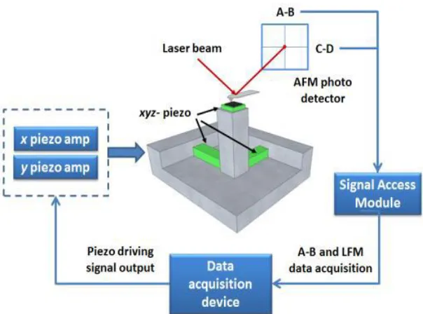
3.1 Experimental platform
AFM is a powerful tool for nanometer scale imaging, measuring, and machining. To obtain the surface information, the sample will be scanned with sharp AFM probe. The
precise imaging in XY direction and z direction is enabled by piezoelectric positioning elements with nanometer scale accuracy. Silicon and silicon nitride is usually used as AFM tip material. During the imaging process, the AFM tip contacts the workpiece surface, and
the deflection of cantilever varies as the height of the workpiece surface varies, which is measured by an optical system. To improve the reflection of laser beam, the AFM cantilever has been coated with a reflective layer, which will reflect the laser beam onto the
photodetector. The topographical and frictional information of sample surface is measured by the displacement of the laser beam on photodetector. In this study, this topographical and
frictional information is collected for cutting force analysis. Park XE-70 is an AFM product from Park Systems, which consists of two independent close-loop XY and Z scanners for the sample and cantilever, a manual coarse stage, and vibration isolation stage. In the AFM
feedback force or distance setting in the XEP software when it moves towards a sample
surface. The maximum measurement range of Z stage is 12 µm. Park XE-70 has two imaging modes, contact mode, and tapping mode. In the following experiments, contact mode is used for nanomachining, while tapping mode is used for imaging before and after machining. The
stage on XY scanner is detachable, so we can put customized nano-vibrator stage onto the XY scanner to provide the XY in-plane vibration.
3.2 Vibration-assisted nanomachining process
For this nanomachining process, the high-frequency XY vibration is introduced to increase the machining controllability as well as improving machining productivity; The
schematic is shown in Figure 3.1. As shown in Figure 3.4, the high-frequency XY in-plane vibration is generated by a nano-vibrator system consisting of two piezoelectric actuators,
which vibrates in two perpendicular directions. The outer edge of the trajectory of the tip circular motion, which is shown in Figure 3.2, can be viewed as a virtual cutting tool with a single tooth whose radius is controlled by the XY vibration amplitude. The schematic is like
single tool fly-cutting in conventional scale. With the assistance of this XY vibration, the width of the machined features can be fully controlled, so unlike the directly scratching
Unlike direct scratching process, with the assistance of XY in-plane vibration, the cutting load is evenly distributed to each rotation cycle. And during each machining cycle,
only a very thin slice of material (defined as feed per rotation) is removed, which is shown in Figure 3.3. In this way, the interaction force is greatly reduced.
3.3 Analysis of the experimental platform
The schematic of the experimental setup is shown in Figure 3.4. The platform is
consisted of a commercial AFM, Park XE-70 (Park Systems Inc) and a lab-designed nano-vibrator system which includes two stack piezo actuators. With the XY nano-nano-vibrator
actuators, high-frequency XY vibration can be provided. Another nano-vibrator actuator, which is attached to the sample, can produce ultrasonic Z vibration. The cutting force signal is acquired by AFM through signal acquisition devices. In this dissertation, only the XY
vibration is applied, and the driving signal is generated from signal generation device. The vibration-assisted nanomachining is performed on PMMA film, which is spin-coated on a
silicon substrate and baked on a hotplate. PMMA is thermoplastic synthesis polymer, and Young’s modulus and shear modulus is 1800-3100 Mpa and 1700 Mpa respectively. The
AFM cantilever used is DLC 190 with tip radius around 30 nm. The A-B, C-D data are
acquired during this machining process.
As mentioned above, the driving signal for XY vibration is generated from signal generation device, the National Instrument USB-6259, which is a multifunction data
acquisition module. This module could provide 4 analog output and 16 analog input channels with 1.25 MS/s sampling rates. The signal processing software, Signal Express, is applied for the output signal control, feedback signal acquisition, and basic signal processing during the
machining process. In our system, NI USB-6259 is used for both signal generation and cutting force data acquisition. Analog output AO 0 generates 2 kHz command signal force
y-axis while AO 3 generates 2 kHz command signal with 90° degree phase difference for X-axis vibration. Combining the vibration from both x-X-axis and y-X-axis, a rotational vibration in XY-plane will be provided. To study the interaction force during machining, we use Signal
Access Module (SAM) from Park Systems to acquire the cantilever deflection signals for both vertical and lateral directions. When an AFM cantilever bends in the vertical direction,
The torsional motions of AFM cantilever, which can reflect the friction between AFM tip
and the workpiece surface, is measured as C-D signal. For our vibration-assisted tip-based nanomachining process, both vertical and lateral motion of AFM cantilever is involved, A-B and C-D data are acquired simultaneously. The raw A-B and C-D voltage signals from
photodetector are collected from SAM.
The surface topography of the workpiece can be imaged by AFM using the tapping
mode, and analyzed using XEI, which is an image process software from Park Systems. Comparing the images of the workpiece surface before and after machining, the feature dimensions, such as depth and width of machined trenches, can be measured. The
nanomachining control is realized in XEL, which is designed for nanolithography applications. A variety of different lithography modes can be achieved using XEL, such as Z
scanner movement mode, Setpoint mode, and Bias mode. During this study, the Setpoint mode is applied to perform nanomachining, and machining parameters, such as setpoint force and feed rate are controlled.
To study the effect of machining parameters, straight trenches are machined. After imaging the workpiece surface before machining, the AFM cantilever is brought to contact
with the workpiece surface under contact mode. To avoid affecting the sample surface as well as the AFM tip, a relatively small setpoint force (e.g. 5 nN) is applied. After approaching, the XEL is set to remote mode, and the AFM is taken over by the XEL
software. Using the XEL interface, the desired patterns can be designed on the loaded pre-scanned image of the workpiece surface, and the cutting force and scan rate can also be set. Then, after clicking the “Start” button, the AFM cantilever will be moved to machine the