Adder structures architecture for deep pipeline & massive parallel Using
SSTA to find ultra-low energy
S. HAROON RASHEED 1& JHANSI PABBATHI 2
1
Associate Professor Dept. of ECE, Svr Engineering College Nandyal Mail: - [email protected]
2
PG-Scholar Dept. of ECE, Svr Engineering College Nandyal Mail: - [email protected]
Abstract
Adders are basic functional units in computer
arithmetic. Binary adders are used in
microprocessor for addition and subtraction
operations as well as for floating point
multiplication and division. Therefore adders
are fundamental components and improving
their performance is one of the major challenges
in digital designs. we have analyzed the latency,
energy consumption, and effects of process
variation on different structures with respect to
the design structure and logic depth to propose
architectures with higher throughput, lower
energy consumption, and smaller performance
loss caused by process variation in application
specific integrated circuit design. We have
exploited adders as different implementations of
a processing unit, and propose architectural
guidelines for finer technologies in subthreshold
which are applicable to any other architecture.
The results show that smaller computing
building blocks have better energy efficiency
and less performance degradation because of
variation effects. In contrast, their computation
throughput will be mid or less unless proper
solutions, such as pipelined or parallel
structures, are used. Therefore, our proposed
solution to improve the throughput loss while
reducing sensitivity to process variations is
using simpler elements in deep pipelined
designs or massively parallel structures.
Keywords: Adder structures, architecture, deep
pipeline, massive parallel, statistical static
timing analysis (SSTA), ultra low energy,
variation-aware.
1.
Introduction
As technology advances, the density of
integrated circuits growsand power consumption
becomes more and more serious [1].
Thisproblem affects the performance of design
and causes heatingand power supply shortage
problems. One major solution is using
near/subthreshold computing to reduce power
consumption over the complex systems-on-chip
[2]. Near and subthreshold computing is
attractive in energy-constrained applications,
such as sensor networks, to increase lifetime and
provide energy harvesting capability for some
emerging applications. In subthreshold region,
both static and dynamic ingredients of power ISWARYA CHINTAKUNTA 2
S. Haroon Rasheed & Iswarya Chintakunta1 2 S. Haroon Rasheed & Iswarya Chintakunta1
2
consumption are severely reduced because of
lower supply voltage. However, circuit delay
grows exponentially by descending voltage
level and hence, the static energy consumption
is increased. In minimum energy point of
energy-voltage curve, this increase in static
energy dominates the dynamic energy
consumption, and scaling supply voltage to
lower levels means more delay and more total
energy consumption [2], [3].
Because of feature size scaling, the impact of
process variations becomes significant and
near/subthreshold design intensifies the effects
of variations and severely degrades the
performance parameters [4]–[6]. In order to
control process variation effects, we need to do
careful timing analysis and employ statistical
approaches rather than the classic worst case
analysis. Static timing analysis (STA) was
previously implemented in commercial tools [7]
and worst case conditions were considered for
each cell timing. Then, cell parameters were
used to calculate delays of paths in a complex
design by adding up delays of gates in series
(n = number of gates)
where μi and δi represent mean and standard
deviation of delay for each gate, respectively. In
new technologies, variation has grown and
using STA yields losing much of the speed
performance, unnecessarily. However, statistical
STA (SSTA) is another way to analyze the
timing specifications of critical paths of a design
for getting more realistic results. Variation of
each cell is assumed as a normal (Gaussian)
variable [5], [8] (2) and (3)1 [9]
The SSTA is an accepted method based on
statistical manner of variations and supported by
recent commercial tools [7], [10]. In this
method, σ /μ [3], [5], [9] is an important ratio to
compare the severity of variations in cells to
have better standard cell design in deep
subthreshold region. Verma et al. [11] extracted
logic chains for Kogge–Stone adder (KSA) to
measure delay variability in both 0.3 and 1.2 V
voltages. σ /μ ratio contours have been drawn
based on delay variability histogram, logic
depth, and gate width, and variability mitigation
is performed by gate up-sizing. Newer
technologies such as dual gate silicon on
insulator [12] have lower variability in
comparison with bulk CMOS to design robust
Thakur et al. [13] analyzed the effects of
variations in gate oxide thickness, supply
voltage, and temperature in four adders and they
tried to rank the variation effect of each
parameter on delay. As a new design method in
[14], SSTA is used to sieve a standard cell
library with different variation constraints
during synthesis of arithmetic circuits. They
have verified the results by Monte Carlo
simulations. Islam et al. [15] have designed a
robust (lower σ /μ ratio) subthreshold full adder
considering power-delay product. Arthurs and
Di [16] evaluate the variations of both
Schmitt-trigger and NULL convention logic 1-bit adders
by four-gate libraries characterized at different
supply voltages for better static noise margin. In
this brief, we use SSTA method to analyze
adder structures considering process variations
and extract effective architectural level design
guidelines to improve speed performance and
energy efficiency.
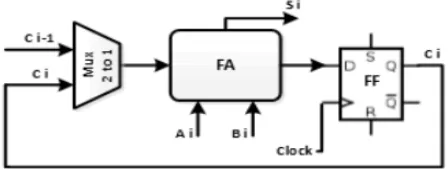
Fig 1. Single-bit full adder in combination with
a flip-flop to do n-bit addition sequentially at
different clock cycles.
2.
Implementation
2.1 Hardware Selection for Energy Efficient
SoC:
2.1.1 Motivation
Many emerging embedded application have
stringent power and energy requirements to
meet battery life and size constraints. An
example application that takes these constraints
to the extremity is long-term medical devices
and wearable devices. Therefore, it is
imperative, when thinking about the architecture
of a SoC and the variety of components on it, to
make judicial decisions to which components to
include so that their energy efficiency is
optimized while still meeting the throughput and
processing capability requirements of the
application. Where in economics we want to
„make every dollar count‟, for a SoC we wish to
„make every pJ count‟. Recent advances in
ultra-low power chip design techniques have
potential to realize a new generation of superior
energy efficient SoCs. However, there remains
the difficulty of determining what combination
of hardware modules maximize energy
efficiency given a variety of application based
processing capabilities, which is the main issue
we deal with in this Chapter. This is especially
true for the digital components on a SoC, as
their selection spreads from the highly flexible
(GPPs) to the highly efficient but non-flexible
ASIC accelerator modules.
2.2 Related Work
The tradeoff between flexibility and efficiency
in hardware is well known and very prominent
in a comparison of conventional hardware
paradigms [12][13]. The most flexible category
of hardware is general purpose processors
(GPPs). GPPs exhibit poor energy efficiency
due to the overhead of fetching and decoding
the instructions that are required to perform a
given operation in the datapath[14].
Sophisticated operations like a fast Fourier
transform (FFT) or data processing algorithm
will thus require numerous instructions in a
simple core. For example, several sub-threshold
processors provide energy per instruction
nearing 1 pJ per operation, but they also tend to
use small instruction sets and thus result in more
instructions to run an operation.
The most efficient hardware is hardwired to do
its specific task or tasks (e.g. ASIC). ASICs
achieve very efficient operation, but they can
only perform the function for which they were
originally defined. Examples of hardwired
implementations in sub-threshold circuits
include [15][16]. Different types of hardware in
sub-threshold systems reveal a similar trend as
their above-threshold counterparts. Some chips
may be implemented as complete ASICs like
JPEG or FFT processors, but more commonly
the case for SoCs, ASICs may appear as
auxiliary hardware accelerator modules,
performing commonly occurring functions in
the context of the larger system. Good examples
of hardware acceleration are multipliers,
floating point units, or FIR filters. These
operations can take several instructions over
many clock cycles to complete using a GPP,
consuming a large amount of energy and time.
A hardware accelerator can process data quickly
and efficiently.
2.3 Hypothesis
We hypothesize that by building a body area
sensor node (BASN) SoC chip that uses
conclusions from a hardware platform
comparison study and whose architecture takes
into account both flexibility and energy
efficiency in data processing, we can achieve a
design geared for a variety of ultra low power
medical applications that consumes minimal
energy that it can operate without a battery, and
solely from an energy harvesting source.
3.
Experimental Work
We have synthesized candidate adders from
register-transfer level to gate level net-lists
using standard synthesis tools. These net-lists
are optimized based on the defined constraints
to achieve maximum working frequency while
initiate the synthesis flow, we have introduced a
custom 20-cell 90-nm CMOS technology library
which is designed for 0.3 V and have
characterized it for different supply voltages
from 0.3 to 1 V at 0.1 V steps. These libraries
are designed using gate sizing with respect to
static noise margin and parameters for local and
global variations. The effects of process
variations on critical path delays are obtained
through Monte Carlo SPICE simulations using
similar gates as load capacitance and the
resulting histogram is fitted to a normal
distribution. Therefore, we compare different
structures based on synthesis and simulation
results. Monte Carlo method simulates the
circuit by sweeping the whole variation
parameters, such as gate oxide thickness,
threshold voltage, and channel length, and does
the measurements for iterations, individually.
Fig 2. Area results normalized to SFA in 90-nm
CMOS.
Fig 3. Critical path delay of different adder
structures in 90-nm CMOS.
Fig 4. Average of maximum latency at different
voltages to do 16-bit addition for different
A. Area
A quick look at Fig. 2 implies that the KSA has
the largest area among all adders, and both HCA
and LFA have the second place. In addition, the
area of RCA structure is the lowest among more
complex ones and is almost 16 times bigger than
serial single full adder (SFA).
B. Performance and Throughput
The critical path delay as speed performance
measure is directly related to the logic depth and
driving fan-outs of internal nodes of structures,
and every increase in these parameters is
translated to more path delay and lower working
frequency. Fig. 3 shows the critical path delays
of all structures in all expected voltage levels,
and confirms our expectation about the fastest
(SFA) and slowest (RCA) adders. The second
place is for BKA (because of more logic depth)
and the third one is for Lander–Fisher due to
higher fan-outs (maximum fan-out for N = 16 is
eight). The comparison between Han–Carlson
and Kogge–Stone shows that the logic depth in
the first one is 20% more, and the working
frequency is almost 10% slower. Calculation of
computational throughput is based on addition
latency for the same size inputs. Fig. 4 shows
the average of maximum latency of different
adders at different voltages to perform
full-length addition of 16-bit operands as a measure
of computation throughput. Obviously,
statistical Monte Carlo analysis has been used
for throughput measurement. As shown, SFA
has higher throughput than RCA adder due to
accumulated delay variation at worst case
design corners for RCA elements, whether the
addition algorithm is the same. The Kogge–
Stone has the best throughput among all
candidates.
4.
Conclusion
In this brief, we have analyzed the latency,
energy consumption, and effects of process
variation on different adder structures as
different implementations of a popular
processing unit with respect to the design
structure and logic depth to propose
architectural guidelines. These guidelines are
applicable to any other architecture without any
dependence to functionality of the design to
achieve higher throughput, lower energy
consumption, and smaller performance loss
caused by process variation in
application-specific integrated circuit design. Simulation
results and analysis confirm that, SFA has
smaller area, less timing fluctuations, and the
highest working frequency, and its throughput is
similar to RCA. Utilizing SFA in parallel
architecture or pipelined version of RCA
improves the throughput besides the energy
efficiency and variation resistance. Therefore, in
increase the throughput/performance of design,
we need to use deeper pipelines such as systolic
arrays or massively parallel designs such as
graphics processing unit structures with simpler
building blocks. Increasing the pipeline depth in
a design causes to break the paths into shorter
sections to increase the throughput and decrease
variations. Simpler computational building
blocks consume lower energy and observe lower
performance variations too. Finally, we
conclude that utilizing such blocks in a
massively parallel architecture is another way to
compensate the process variation effects and
lower the frequency uncertainty plus lowering
timing fluctuations due to process variations.
5. References
[1] M. B. Taylor, “A landscape of the new dark silicon design regime,” IEEE Micro, vol. 33, no.
5, pp. 8–19, Sep./Oct. 2013.
[2] A. Wang, B. H. Calhoun, and A. P.
Chandrakasan, Sub-Threshold Design for Ultra
Low-Power Systems. New York, NY, USA:
Springer-Verlag, 2006.
[3] Z. Bo et al., “Energy-efficient subthreshold
processor design,” IEEE Trans. Very Large
Scale Integr. (VLSI) Syst., vol. 17, no. 8, pp.
1127–1137, Aug. 2009.
[4] H. Iwai, “Roadmap for 22 nm and beyond (Invited Paper),” Microelectron. Eng., vol. 86,
nos. 7–9, pp. 1520–1528, 2009.
[5] International Solid State Circuits Conference
2013 Trends. [Online]. Available:
http://isscc.org/doc/2013, accessed 2014.
[6] X. Chen, L. Yang, R. P. Dick, L. Shang, and
H. Lekatsas, “C-pack: A high-performance
microprocessor cache compression algorithm,”
IEEE Trans. Very Large Scale Integr. (VLSI)
Syst., vol. 18, no. 8, pp. 1196–1208, Aug. 2010.
[7] Synopsys On-Line Documents. [Online].
Available: http://www.
synopsys.com/support/pages/dow.aspx,
accessed 2014.
[8] A. Srivastava, D. Sylvester, and D. Blaauw,
Statistical Analysis and Optimization for VLSI:
Timing and Power. New York, NY, USA:
Springer-Verlag, 2006.
[9] S. R. Sarangi, B. Greskamp, R. Teodorescu,
J. Nakano, A. Tiwari, and J. Torrellas,
“VARIUS: A model of process variation and
resulting timing errors for microarchitects,”
IEEE Trans. Semicond. Manuf., vol. 21, no. 1,
pp. 3–13, Feb. 2008.
[10] M. Tehranipoor, K. Peng, and K.
Small-Delay Defects. New York, NY, USA:
Springer-Verlag, 2011.
[11] N. Verma, J. Kwong, and A. P.
Chandrakasan, “Nanometer MOSFET variation
in minimum energy subthreshold circuits,”
IEEE Trans. Electron Devices, vol. 55, no. 1,
pp. 163–174, Jan. 2008.
[12] R. Vaddi, S. Dasgupta, and R. P. Agarwal,
“Device and circuit co-design robustness studies
in the subthreshold logic for ultralow-power
applications for 32 nm CMOS,” IEEE Trans.
Electron Devices, vol. 57, no. 3, pp. 654–664,
Mar. 2010.
[13] A. Thakur, D. Chilamakuri, and D. Velenis,
“Effects of process and environmental
variations on adder architectures,” in Proc. 49th
IEEE Int. Midwest Symp. Circuits Syst.
(MWSCAS), Aug. 2006, pp. 36–40.
[14] J. Crop, R. Pawlowski, N. Moezzi-Madani,
J. Jackson, and P. Chaing, “Design automation
methodology for improving the variability of
synthesized digital circuits operating in the
sub/near-threshold regime,” in Proc. Int. Green
Comput. Conf. Workshops (IGCC), Jul. 2011,
pp. 1–6.
[15] A. Islam, A. Imran, and M. Hasan, “Robust
subthreshold full adder design technique,” in
Proc. Int. Conf. Multimedia, Signal Process.
Commun. Technol. (IMPACT), Dec. 2011, pp.
99–102.
[16] A. Arthurs and J. Di, “Analysis of ultra-low
voltage digital circuits over process variations,”
in Proc. IEEE Subthreshold Microelectron.
Conf. (SubVT), Oct. 2012, pp. 1–3.
[17] M. Talsania and E. John, “A comparative
analysis of parallel prefix adders,” in Proc. Int.
Conf. Comput. Design, Las Vegas, NV, USA,
Jul. 2013, pp. 29–36.
[18] B. Parhami, Computer Arithmetic:
Algorithms and Hardware Designs. London,
U.K.: Oxford Univ. Press, 2009.
[19] K. T. Johnson, A. R. Hurson, and B.
Shirazi, “General-purpose systolic arrays,”
IEEE Comput., vol. 26, no. 11, pp. 20–31, Nov.
1993.
[20] M. Bekakos, I. Ž. Milovanovi´ c, T. I.
Toki´ c, C. B. Doli´ ´ canin, and E. I.
Milovanovi´ c, “Selecting mathematical method
for systolic processing,” Sci. Pub. State Univ.
Novi Pazar A, Appl. Math., Inf. Mech., vol. 3,