Improved Evaluation Method for the SRAM Cell Write
Margin by Word Line Voltage Acceleration
*
Hiroshi Makino1, Naoya Okada2, Tetsuya Matsumura3, Koji Nii4, Tsutomu Yoshimura5, Shuhei Iwade1, Yoshio Matsuda2
1Faculty of Information Science and Technology, Osaka Institute of Technology, Hirakata, Japan 2Graduate School of Natural Science, Kanazawa University, Kanazawa, Japan
3SoC Software Platform Division, Renesas Electronics Corporation, Itami, Japan 4Design Platform Development Division, Renesas Electronics Corporation, Kodaira, Japan
5Faculty of Engineering, Osaka Institute of Technology, Osaka, Japan
Email: {makino, iwade}@is.oit.ac.jp, {me111358, matsuda}@ec.t.kanazawa-u.ac.jp, {tetsuya.matsumura.zg, koji.nii.uj}@renesas.com, [email protected]
Received April 14,2012; revised May 14, 2012; accepted May 21, 2012
ABSTRACT
An accelerated evaluation method for the SRAM cell write margin is proposed using the conventional Write Noise Margin (WNM) definition based on the “butterfly curve”. The WNM is measured under a lower word line voltage than the power supply voltage VDD. A lower word line voltage is chosen in order to make the access transistor operate in the saturation mode over a wide range of threshold voltage variation. The final WNM at the VDD word line voltage, the Accelerated Write Noise Margin (AWNM), is obtained by shifting the measured WNM at the lower word line voltage. The WNM shift amount is determined from the measured WNM dependence on the word line voltage. As a result, the cumulative frequency of the AWNM displays a normal distribution. Together with the maximum likelihood method, a normal distribution of the AWNM drastically improves development efficiency because the write failure probability can be estimated from a small number of samples. The effectiveness of the proposed method is verified using the Monte Carlo simulation.
Keywords: Static Random Access Memory (SRAM); Write Noise Margin (WNM); Vth Fluctuation; Variance; WNM Distribution
1. Introduction
The recent progress of process technology has caused various fluctuation problems in device characteristics due to transistor area reduction. The threshold voltage (Vth) fluctuation caused by dopant fluctuation strongly influ- ences device characteristics [1,2]. Generally, this dopant induced Vth fluctuation is random and obeys a normal distribution.
The stability of SRAM cells is greatly affected by Vth fluctuation, because SRAM cells are usually designed using minimum design rules. Vth fluctuation degrades both the read and the write operation stabilities. It is said that the read operation is usually more critical than the write operation under Vth fluctuation. However, the write operation is also affected by a large Vth fluctuation. In addition, a recent paper indicates that write operation
failure is more dominant than read operation failure un- der low supply voltage conditions [3]. Therefore, an ac- curate evaluation of write operation stability is as impor- tant as an evaluation of read operation stability.
Conventionally, the Write Noise Margin (WNM), based on the “butterfly curve”, is used as a metric of write operation stability [4]. Since the write operation is strongly affected by the Vth of the SRAM cell access transistors, the conventional WNM is also expected to be sensitive to Vth variation of the SRAM cell access tran- sistors. However, the WNM is not sensitive to Vth varia- tion when the WNM is large. In addition, the WNM does not obey a normal distribution. Takeda et al. described these problems and maintained the importance of a nor- mal distribution of the WNM [5]. They proposed a new write margin definition which is sensitive to Vth varia- tion of the access transistors and follows a normal distri- bution. Recently, several new definitions have been pro- posed [6-9]. If the write margin obeys the normal distri- bution, the write margin distribution can be easily esti-
*Several parts of this paper are based on the authors’ previous work
mated by a small number of samples [5]. This drastically improves development efficiency, especially when com- bined with the maximum likelihood method.
In this paper, we propose an accelerated evaluation method for the SRAM cell write margin using the con-ventional butterfly curve based WNM definition. The WNM is measured at a lower word line voltage than the power supply voltage VDD and calibrated to the WNM of the VDD word line voltage. In the proposed method, the write margin obeys the normal distribution even un-der the conventional WNM definition.
In Section 2, the reason why the conventional WNM does not obey the normal distribution is analyzed. In Sec- tion 3, an accelerated evaluation method for the SRAM cell write margin is proposed based on the analysis in Section 2. In Section 4, the proposed method is verified using the Monte Carlo simulation. Finally, Section 5 provides the conclusion.
2. Conventional Write Noise Margin
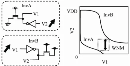
A diagram of the SRAM write operation circuit is shown in Figure 1. Let us assume that the inverted data are written to the SRAM cell where “1” is stored on the in- ternal node V1 and “0” on the V2. Then, the data “0” and “1” are given on bit lines BL and /BL, respectively, un- der the activated word line WL. If the voltages of nodes V1 and V2 are inverted, the write operation is successful. Hereupon, V1, V2, BL, /BL and WL represent the volt- ages.
The definition of the conventional Write Noise Margin (WNM) based on the butterfly curve is shown in Figure 2. We draw the DC transmission curves of inverter A (InvA in Figure 1) and inverter B (InvB in Figure 1) under WL = VDD, BL = 0 V and /BL = VDD. The VDD is the power supply voltage. The WNM is defined as the width of the smallest embedded square between the two DC transmission curves.
[image:2.595.70.277.571.710.2]Generally, the write margin is a function of the thresh- old voltage Vth’s of the six transistors in a SRAM cell. If
Figure 1. Diagram of the SRAM cell circuit of the write operation.
the write margin is linear on the Vth’s, the write margin is expected to obey the normal distribution, allowing us to predict the write margin distribution accurately from a small number of samples. Furthermore, if the write mar-gin distribution is the normal distribution, the write yield can also be easily estimated [10].
The dependence of the WNM on the Vth is examined using the SPICE simulation. The transistor parameter of 45-nm process technology [11] is used with the power supply voltage of VDD = 1.0 V. The threshold voltages are the typical values of Vthn = 0.404 V for the NMOS transistors and Vthp = –0.384 V for the PMOS transistors. The transistor sizes are L = 45 nm and W = 55 nm, 83 nm, and 55 nm with for the access, driver, and load tran- sistors, respectively.
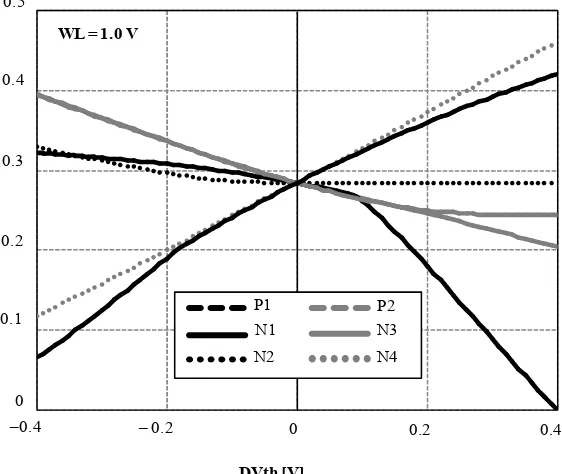
The simulation results are shown in Figure 3. We set
ΔVth = 0, a typical threshold voltage. The WNM is not linear on the Vth of the access transistor N1. However, the WNM is almost linear on the other transistors. The nonlinearity on access transistor N1 causes the WNM to deviate from the normal distribution [10]. In the lower Vth region, the load transistor P1 determines WNM = 0, that is, the write limit. In the higher Vth region, the ac- cess transistor N1 determines the write limit. The slope of the WNM for the N1 changes significantly near ΔVth = 0.1 V. The WNM is completely linear for ΔVth > 0.1 V. We call this area the linear section of the WNM for the N1. WNM = 0 is on this straight line. When ΔVth < 0.1 V, the slope of the WNM is almost equal to 0. This means that the WNM is not sensitive to Vth variation of the N1 when the WNM is large. This is consistent with previous research [5]. The access transistors only affect the WNM in the case of a large Vth variation. In other words, the WNM distribution has a tail at the side of the small margin. A large number of samples is needed in order to estimate the distribution. If we estimate the dis- tribution with a small number of samples, with many appearing around ΔVth = 0, the predicted distribution is very sharp. This results in an overestimation of ΔVth for WNM = 0, because the slope of the WNM is nearly equal to 0 around ΔVth = 0.
[image:2.595.317.529.609.717.2]The reason why the WNM has different slopes around
Figure 2. Definition of the Write Noise Margin (WNM).
ΔVth = 0.1 V can be explained by a change in the opera- tion mode of the access transistors when the WNM is evaluated. The dependence of the V1 on the ΔVth of N1 in Figure 1 is examined using the SPICE simulation at V2 = 0 V. The results are shown, together with the WNM, in Figure 4. The dashed line, which is determined by the equation V1 = VDD-Vth, represents the boundary of the operation mode of the access transistor N1. In the region to the left of the dashed line, the N1 operates in the linear mode and to the right of the dashed line, it operates in the saturation mode. Therefore, the operation mode of the access transistor changes around the point where the V1 curve intersects with the dashed line. The changing point
of the WNM slope, which is around ΔVth = 0.1 V, closely corresponds to the changing point of the operation mode of the access transistor. Thus, a change in the slope of the WNM is strongly related to a change in the operation mode of access transistor N1.
In the AC write operation of a SRAM cell, access transistor N1 is always in the saturation mode at the be- ginning of the write operation because the V1 is not lower than the WL. Write failure occurs when the N1 stays in the saturation mode during the write operation. Therefore, the write margin should be evaluated in the saturation mode of access transistor N1. Contrary to the actual AC write operation, the conventional WNM is
DVth [V]
N4 N2
WL = 1.0 V
WNM
[V
]
P2 N3 N1
P1 0.1
0.2 0.3 0.4 0.5
0.4 0
[image:3.595.142.465.254.693.2]–0.4 – 0.2 0 0.2
Figure 3. Dependence of the WNM on the ΔVth at WL = VDD.
–0.6 –0.4 –0.2 0 0.2 0.4 0.6
0 0.05 0.1 0.15 0.2 0.25 0.3 0.35 0.4
0 0.25 0.5 0.75 1
V1 WNM
Linear Mode
DVth [V]
WN
M
[V
]
V1
[V]
Saturation Mode
Figure 4. Dependence of the WNM and V1 at a fixed voltage of V2 = 0 V on the threshold voltage variation of the access tran- istor N1 in the write operation.
[image:3.595.175.456.257.494.2]evaluated in the linear mode of the access transistor when the write margin is large. Using the conventional WNM definition, therefore, is not an effective way to evaluate the stability of a SRAM cell.
3. Accelerated Evaluation Method
In this section, we propose an accelerated evaluation method for the SRAM cell write margin based on the conventional WNM definition. In the proposed method, the access transistor is forced to operate in the saturation mode by lowering the word line voltage from the VDD. The WNM is then measured under the lower word line voltage. The word line voltage is chosen from a range which causes the access transistor to operate in the satu- ration mode. The WNM at the word line voltage of the VDD is calibrated from the measured WNM at the lower word line voltage. This calibrated WNM is called the Accelerated WNM (AWNM).
First, we measure the dependence of the WNM on the word line voltage. The WNM given by the SPICE simula- tion is shown in Figure 5. The power supply voltage is VDD = 1.0 V. The solid line represents the simulation results. The WNM is linear for a word line voltage of less than 0.9 V, meaning that the access transistor N1 operates in the saturation mode in this range of word line voltages, the equivalent of a high ΔVth. The slope change of the WNM at the word line voltage of 0.9 V corre- sponds to a change in the operation mode of the access transistor N1 around the threshold voltage of ΔVth = 0.1 V in Figure 4. The operation mode of the N1 moves to the linear mode in WL > 0.9 V.
Although the accelerated evaluation method using a word line voltage below 0.9 V gives a good linearity for the WNM, the value of the WNM itself is small when compared to the WNM at WL = 1.0 V. This is because
the WNM is evaluated at a lower word line voltage. Therefore, this value is calibrated to the WNM at WL = 1.0 V. The dashed line in Figure 5 represents the ex- trapolated line. The extrapolated value of the WNM us ing the straight line is 0.35 V, the WNM at WL = 1.0 V, which is the AWNM in the proposed method.
In the accelerated evaluation method, the AWNM at WL = 1.0 V, denoted as AWNM (WL1.0), is obtained
from the measured WNM at a low word line voltage, the WNM (WLm), as:
1.0
m
1.0 m
AWNM WL WNM WL WL WL , [image:4.595.151.453.524.718.2](1) where α is the slope of the WNM for the WL voltage in the linear section. This AWNM is considered to be the write margin corresponding to the AC write operation.
Figure 6 shows the dependence of the WNM on the
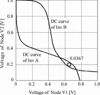
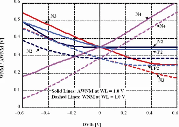
ΔVth at the word line voltage of 0.8 V. A negative value is defined as the maximum length of an embedded square in the crossed curves, as shown in Figure 7. This means that the data are not inverted. In Figure 6, the slope changing point of the WNM for the N1 moves to the left when compared to the slope changing point under the word line voltage of 1.0 V (Figure 3). As a result, the measured samples around ΔVth = 0 V are in the linear section. In Figure 8, the dependence of the WNM and AWNM on the ΔVth’s is shown for access transistor N1 and load transistor P1. The solid lines are the AWNM and the dashed lines are the WNM. The extrapolated lines are drawn from the AWNMs around ΔVth = 0 V. The extrapolated line for access transistor N1 gives the correct write limit because the threshold voltage ΔVth at AWNM = 0 predicted by the extrapolated line is the same as the ΔVth at WNM = 0. This means that meas- ured samples around ΔVth = 0 V for the N1 predict the
0.7 0.75 0.8 0.85 0.9 0.95 1.0
0 0.1 0.15 0.2 0.25 0.3 0.35 0.4
WN
M
[V
]
Word Line Voltage [V]
AWNM
0.05
Figure 5. Dependence of the WNM on the word line voltage.
DVth [V]
WNM
[V
]
WL=0.8 V
–0.1
–0.2 0 0.1 0.2 0.3
–0.4 –0.2 0 0.2 0.4
N4 N2
N3 N1
P2 P1
[image:5.595.149.465.87.329.2]0.4
Figure 6. Dependence of the WNM on ΔVth under WL = 0.8 V.
Figure 7. The butterfly curve with a negative write margin when ΔVth = 0.2 V for the N1 and ΔVth = 0 V for other transistors (see Figure 6).
correct write limit if the AWNM is used as a metric. As for load transistor P1, there is a slight difference between the write limit of the WNM and the write limit predicted from the AWNM around ΔVth = 0. The extrapolated line for the P1 gives about a 0.1 V higher ΔVth value than the WNM for the write limit. This means that the AWNM predicts a slightly lower write limit for the Vth variation of the P1. The absolute value of the predicted ΔVth at AWNM = 0 for access transistor N1 is smaller than the absolute value for load transistor P1. Therefore, when the AWNM is used as a metric, the Vth variation of the N1 has the strongest influence on the write operation while the influence of the P1 is relatively small. Furthermore,
the write limit predicted by the AWNM is always in the safer side, because the absolute value of the predicted write limit for the P1 variation is always lower than the write limit in the WNM.
The AWNM and the WNM are shown for the other transistors in Figure 9. These transistors have only a small influence on the write limit because the absolute
ΔVth values at AWNM = 0 are far larger than those for the N1 and the P1 shown in Figure 8.
4. Monte Carlo Simulation
The proposed method is verified using the Monte Carlo simulation. The Vth’s are assumed to follow the normal distribution with a variance of σVth = 50 mV and a mean
of Vthn = 0.404 V and Vthp = –0.384 V. In the Monte Carlo simulation, we make the Vth’s of six SRAM cell transistors independently change at random. The number of samples is 100,000. For simplicity, we set the same variance for every transistor.
[image:5.595.89.256.364.522.2]Figure 8. Dependence of the AWNM and the WNM at WL = 1.0 V on the ΔVth of access transistor N1 and load transistor P1.
Figure 9. Dependence of the AWNM and the WNM at WL = 1.0 V on the ΔVth of transistors N2, N3, N4, and P2.
such devices is very small. The dependence of the WNM on the word line voltage is shown for the first ten sam- ples in Figure 10. The slopes α = ΔWNM/ΔWL are al- most the same for the ten samples in each linear section. A word line voltage can be chosen, such as 0.7 V or 0.8 V, from these data. The cumulative frequency scaled by the variance σ is shown in Figure 11. A straight line for the cumulative frequency indicates a normal distribution of the write margin. Lines I, II, and III are the WNM at WL = 0.7 V, 0.8 V, and 1.0 V, respectively. Line IV is the AWNM corresponding to WL = 1.0 V calibrated from line I, that is, the WSNM at WL = 0.7 V. Line V is
the AWNM corresponding to WL = 1.0 V calibrated from line II, that is, the AWNM at WL = 0.8 V. For the calibration, we use α = 1.060, which is the mean value of the ten samples. The mean values of the WNM and AWNM, μWNM and μAWNM, are summarized in Table 1.
The two means of the AWNM at WL = 1.0 V, calibrated from the WNM at WL = 0.7 V and WL = 0.8 V, are very similar. Lines IV and V of the AWNMs at WL = 1.0 V, calibrated from I and II, respectively, almost overlap, demonstrating the validity of the proposed method.
The slope of the cumulative frequency of the conven- tional WNM at WL = 1.0 V (line III in Figure 11)
[image:6.595.143.454.336.557.2]Figure 10. Dependence of the WNM on the word line volt- age for the first ten samples in the Monte Carlo simulation.
Figure 11. The cumulative frequency of the AWNM and the WNM. Lines I, II and III are the WNM at WL = 0.7 V, 0.8 V, and 1.0 V, respectively. Lines IV and V are the AWNM at WL = 1.0 V calibrated from lines I and II, respectively. The IV and V lines almost overlap.
Table 1. The mean values of the WNM and AWNM.
μWNM [V] μAWNM [V]
WL = 0.7 V 0.0355 0.354
WL = 0.8 V 0.144 0.356
WL = 1.0 V 0.284
changes at about WNM = 0.2 V. There are two slopes corresponding to the two operation modes of access tran- sistor N1, as discussed in Section 2. Obviously, the con- ventional WNM does not obey the normal distribution. Therefore, the WNM at WL = 1.0 V gives a low write failure probability if the probability is estimated from a slope in the vicinity of ΔVth = 0 V. On the other hand, the cumulative frequency of the WNM at WL = 0.7 V and WL = 0.8 V are straight lines. This means that the frequencies follow the normal distribution. The slopes of the extrapolated lines are almost the same. As a result, both the AWNMs (lines IV and V) follow the normal
distribution. Their slopes are the same as that of the con-ventional WNM in the small WNM region below 0.2 V, because the access transistor operates in the saturation mode in this region. The extrapolated σ values at AWNM = 0 of the cumulative frequency of the AWNMs coincide with the σ value at WNM = 0 extrapolated from the lin- ear section in the small WNM region, as shown in Fig- ure 11. Table 2 summarizes the values of –WM WM
which correspond to the extrapolated cumulative fre- quency at WM = 0 in the scale of σ. Hereupon, we will use write margin (WM) as a general designation. There are two –WM WM’s in the conventional WNM based on
the two slopes in the cumulative frequency. Because the cumulative frequencies, IV and V in Figure 11, nearly overlap, the –WM WM’s for the two AWNMs calibrated
from WL = 0.7 V and WL = 0.8 V are almost the same. If the WM obeys the normal distribution, the write failure probability PWF of writing “0” to the left-side
storage node V1 in Figure 1 is given as:
WM WM
2 WM 2 WM WM
WM
1 exp dWM
2 2π
WF
P
(2)
μWM and σWM are the mean and the variance of the WM
distribution, respectively. By using the variable trans- formation x
WMWM
WM , we obtain the fol-lowing equation:WM WM 1 x2
exp dx
2 2π
WF
P
W
Y 1 2PWF
(3)
The write failure probability of writing “1” is equal to the write failure probability of writing “0” due to SRAM cell symmetry. Furthermore, the cases of writing “0” error and writing “1” error are considered to be almost exclusive to each other. Thus, write yield YW is given as:
(4)
If the distribution of the WM is not guaranteed to be the normal distribution, it is very difficult to estimate the write yield because the distribution cannot be generally determined by only the measured data.
Table 3 shows the linearly extrapolated –WM WM and
Table 2. Extrapolated values of –μWM σWM giving WM = 0
in Figure 11.
WM WM
–
WNM –8.58*/–6.08**
AWNM at WL = 1.0 V from WL = 0.7 V –5.72 AWNM at WL = 1.0 V from WL = 0.8 V –5.78
*The extrapolated value as a straight line with the slope of the WNM around
the mean value of 0.28 V. **The extrapolated value as a straight line with the
[image:7.595.56.288.519.578.2] [image:7.595.308.539.645.703.2]CS Table 3. Extrapolated write limits and PWF’s of the WNM
and the AWNMs.
AWNM WNM
from 0.7 V from 0.8 V CWLM [10]
–WM WM –8.24 –5.72 –5.78 –5.71
PWF [ppm] 8.61 × 10⁻¹¹ 5.33 × 10⁻³ 3.74 × 10⁻³ 5.65 × 10⁻³
Copyright © 2012 SciRes. the write failure probability (PWF) for the data in Figure
11. PWF’s are calculated from each –WM WM using
Equation (3). In Table 3, the –WM WM and PWF val-
ues in the definition proposed by Gierczynski et al. [6] are also shown as a reference [10]. We call this write margin the CWLM (Combined Word Line Margin). The CWLM not only gives the correct write limit, but also displays good linearity in the cumulative frequency and, therefore, obeys the normal distribution, as discussed in detail in [10].
The extrapolated –WM WM values of the AWNM
from the WNM at WL = 0.7 V and WL = 0.8 V are nearly equal within a deviation of 1.05%. Therefore, the predicted PWF’s are very similar to each other within a
factor of 1.43. Furthermore, the extrapolated –WM WM
used for the proposed ac- ce
values in the AWNMs also clearly match the values in the CWLM. This means that the AWNMs calibrated from the WNM at WL = 0.7 V and WL = 0.8 V give suf-
ficiently accurate PWF’s. In SRAM design, predicting the
order of the PWF is important for determining the redun-
dancy circuit. Therefore, obtaining an accurate PWF using
the AWNM is valuable. Thus, the butterfly curve based WNM is still effective when
[image:8.595.71.529.410.693.2]lerated evaluation method.
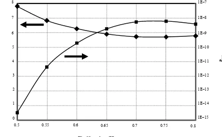
Figure 12 shows the dependence of the WM WM
of AWNM and the calculated PWF on the word -
age at which the WNM is measured. The
line volt
WM WM
value stays almost constant for a word line voltage higher than 0.65 V, resulting in similar PWF values within the
same order of m in this word line voltage region. However, the
agnitude
WM WM
increases for a word line volt- age below 0.65 V, resulting in a rapid decrease in the PWF.
This is because the off-state access transistor appears at the low word line voltage. If the Vth of the access tran- sistor deviates to high, it turns off at the low word line voltage. When the access transistor turns off, the linearity of the WNM for the word line voltage is lost. Therefore, a WNM measured with an off-state access transistor does not follow the normal distribution. As the word line volt- age decreases below 0.65 V, the number of samples with such off-sta transistors rapidly increases. As a result, the
te access
WM WM
and PWF values deviate from the
correct value. In this case, a word line voltage from 0.65 V to 0.8 V is suitable to evaluate the AWNM.
Word line voltage [V] 0.5
μWM
/
σWM
1E–7
0.8
PWF
1E–8
1E–9
1E–10
1E–11
1E–12
1E–13
1E–14
1E–15
0.55 0.65 0.7 0.75
8
7
6
5
4
3
2
1
0
0.6
Figure 12. Dependence of the μWM σWM of the AWNM and the calculated PWF on the word line voltage at which the WNM
If the WM is guaranteed to obey the normal distribu- io
t n, the variance and the mean can be easily estimated from a small amount of data. According to the maximum likelihood method, the mean μWM and the variance σWM
are obtained from the write margin WMj data, with an
error of order 1 N as:
WM j
j
WM N
1
(5)
2j WM
WM
. (6)
In Tables 4-6, the variance and the m fr
]
2
WM j
1 N
ean obtained om (5) and (6) using the Monte Carlo simulation data are summarized. Table 4 shows the case of a conven-
Table 4. The mean and variance of the WNM at V = 1.0 V in the Monte Carlo simulation.
μWM [V] σWM [V WM WM PWF [ppm]
N = 100 0.305 0.0395 7.73 5.38 × 10⁻⁹
N = 300 0.302 0.0368 8.19 1.31 × 10⁻¹⁰
N = 1000 0.305 0.0385 7.93 1.10 × 10⁻⁹
N = 3000 0.306 0.0369 8.20 1.20 × 10⁻¹⁰
N = 10,000 0.306 0.0374 8.12 2.33 × 10⁻¹⁰
N = 30,000 0.306 0.0376 8.14 1.98 × 10⁻¹⁰
N = 100,000 0.306 0.0374 8.18 1.42 × 10⁻¹⁰
able 5. The mean and variance of the AWNM at WL = 1.0
M ]
T
V calibrated from the WNM at WL = 0.7 V in the Monte Carlo simulation.
μW [V] σWM [V WM WM PWF [ppm]
N = 100 0.340 0.0591 5.76 4.21 × 10⁻³
N = 300 0.342 0.0588 5.81 3.12 × 10⁻³
N = 1000 0.345 0.0603 5.72 5.33 × 10⁻³
N = 3000 0.345 0.0596 5.79 3.52 × 10⁻³
N = 10,000 0.346 0.0602 5.75 4.46 × 10⁻³
N = 30,000 0.346 0.0607 5.70 5.99 × 10⁻³
N = 100,000 0.347 0.0606 5.72 5.33 × 10⁻³
Table 6. The mean and variance of the AWNM at WL = 1.0
M ]
V calibrated from the WNM at WL = 0.8 V in the Monte Carlo simulation.
μW [V] σWM [V WM WM PWF [ppm]
N = 100 0.348 0.0607 5.74 4.46 × 10⁻³
N = 300 0.349 0.0589 5.92 1.61 × 10⁻³
N = 1000 0.352 0.0602 5.85 2.46 × 10⁻³
N = 3000 0.352 0.0591 5.95 1.34 × 10⁻³
N = 10,000 0.353 0.0597 5.92 1.61 × 10⁻³
N = 30,000 0.353 0.0603 5.86 2.31 × 10⁻³
N = 100,000 0.354 0.0600 5.89 1.93 × 10⁻³
tional WNM at WL = 1.0 V. In this table, the WM WM is
la t N ,00 co t r
that the w rge, even a = 100 0, when mpared o the othe extrapolated values in Table 3. This shows rite failure probability is underestimated in the conventional WNM, even when N = 100,000 is used. Table 5 shows the case of the AWNM at WL = 1.0 V calibrated from the WNM at WL = 0.7 V. Because the AWNM obeys the normal distribution, a close agreement is observed between a value with a small N, for example, N = 100, 300, etc., and a value with N = 100,000 or an extrapolated value in
Table 3. Also, the calculated PWF for every N is close to
that of the CWLM in Table 3 within a factor of 1.81. This means that a sufficiently accurate write failure probability can be easily predicted from a small number of measured samples. Table 6 shows the AWNM at WL = 1.0 V calibrated from the WNM at WL = 0.8 V. In this case, although the WM WM is close to the extrapolated
value in Table 3 for only N = 100, it becomes slightly larger for N > 100. As a result, the calculated PWF’s for N
> 100 are smaller than the values in Table 5, creating an increase in the deviation from the PWF’s of the CWLM in
Table 3. The reason for such deviation can be explained by the sample which is produced when the access tran- sistor is operating in the linear mode. When the Vth of an access transistor becomes low, the access transistor oper- ates in the linear mode under a relatively lower word line voltage. In Figure 10, we can see that one of the ten samples begins to deviate from the linear section above the word line voltage of 0.85 V. This sample is thought to have a low-Vth access transistor. If the number of samples increases, samples with access transistors oper- ating in the linear mode under a word line voltage of less than 0.8 V will appear. Such samples deviate from the normal distribution. We can observe this phenomenon in
Figure 11 as a deviation from the linearity of Line V in the high WM region.
Although the PWF’s in Table 6 are still useful for pre-
dicting the write failure probability because they are in the same order as the write failure probability of the CWLM in Table 3, the PWF’s in Table 5 are more accu-
rate. Therefore, 0.7 V should be chosen as the word line voltage at which the WNM is measured. This can be eas- ily done by finding the center of the word line voltage region in which every sample is in the linear section, in
Figure 10. By using an appropriate word line voltage, the proposed method allows us to predict the correct write failure probability from a small number of meas- ured samples. This provides a drastic improvement in development efficiency.
5. Conclusion
We have proposed an accele the SRAM cell wr
word line voltage than the VDD of the power supply voltage, forcing the access transistor to operate in the saturation mode. The Accelerated Write Noise Margin (AWNM), the WNM at WL = VDD in this method, is obtained by shifting the WNM at the lower word line voltage. The extent of the shift is determined from the WNM dependence on the word line voltage. The effec- tiveness of the proposed accelerated evaluation method for the write margin is verified using the Monte Carlo simulation. The cumulative frequency of the AWNM is linear, indicating a normal distribution. Together with the maximum likelihood method, the normal distribution of the AWNM dramatically improves development effi- ciency, because the write failure probability can be esti- mated using a small number of samples.
REFERENCES
[1] M. J. M. Pelgrom, A. C. J. Duinmaijer and A. P. G
bers, “Matchi Transistors,”
Journal of Sol 4, No. 5, 1989, pp.
. Wel-
IEEE
ng Properties of MOS
id-State Circuits, Vol. 2 1433-1440.doi:10.1109/JSSC.1989.572629
[2] P. A. Stolk, F. P. Widdershoven and D. B. M. Klaassen, “Modeling Statistical Dopant Fluctuations in MOS Tran- sistors,” IEEE Transactions on Electron Devices, Vol. 45, No. 9, 1998, pp. 1960-1971.doi:10.1109/16.711362 [3] O. Hirabayashi, A. Kawasumi, A. Suzuki, Y. Takeyama,
K. Kushida, T. Sasaki, A. Katayama, G. Fukano, Y. Fu- jimura, T. Nakazato, Y. Shizuki, N. Kushiyama and T. Yabe, “A Process-Variation-Tolerant Dual-Power-Supply SRAM with 0.179 um2 Cell in 40 nm CMOS Using Level
Programmable Wordline Driver,” ISSCC Digg Technol- ogy Papers, 2009, pp. 458-459.
[4] A. Bhavnagarwala, S. Kosonocky, C. Radens, K. Stawi- asz, R. Mann, Q. Ye and K. Chin, “Fluctuation Limits &
Scaling Opportunities for CMOS SRAM Cells,” ISSCC Digg Technology Papers, 2005, pp. 659-662.
[5] K. Takeda, H. Ikeda, Y. Hagihara, M. Nomura and H. Kobatake, “Redefinition of Write Margin for Next-Gen-
ined Methodology for Write-Margin Extraction of eration SRAM and Write-Margin Monitoring Circuit,”
IEEE ISSCC, Digest of Technology Papers, 2006, pp. 630- 631.
[6] N. Gierczynski, B. Borot, N. Planes and H. Brut, “A New Comb
Advanced SRAM,” IEEE International Conferences on Microelectronic Test Structure, 19-22 March 2007, pp. 97- 100.doi:10.1109/ICMTS.2007.374463
[7] K. Zhang, U. Bhattacharya, Z. Chen, F. Hamzaoglu, D. Murray, N. Vallepalli, Y. Wang, B. Zheng and M. Bohr, “A 3-GHz 70-Mb SRAM in 65-nm CMOS Technology with Integrated Column-Based Dynamic Power Supply,”
IEEE Journal of Solid-State Circuits, Vol. 41, No. 1, 2006, pp. 146-151.doi:10.1109/JSSC.2005.859025
[8] C. Wann, R. Wong, D. Frank, R. Mann, S.-B. Ko, P. Croce, D. Lea, D. Hoyniak, Y.-M. Lee, J. Toomey, M.
r Weybright and J. Sudijono, “SRAM Cell Design for Sta- bility Methodology,” 2005 IEEE VLSI-TSA International Symposium on VLSI Technology, April 2005, pp. 21-22. [9] E. Grossar, M. Stucchi, K. Maex and W. Dehaene, “Read
Stability and Write-Ability Analysis of SRAM Cells fo Nanometer Technologies,” IEEE Journal of Solid-State Circuits, Vol. 41, No. 11, 2006, pp. 2577-2588.
doi:10.1109/JSSC.2006.883344
[10] H. Makino, S. Nakata, H. Suzuki, S. Mutoh, M. T. Yoshimura, S. Iwade and Y. M
Miyama, atsuda, “Reexamination of SRAM Cell Write Margin Definitions in View of Pre- dicting Distribution,” Transactions on Circuits and Sys- tems II: Brief Express, Vol. 58, No. 4, 2011, pp. 230-234. [11] Visit, “45 nm PTM HP Model: V2.1.”
http://www.eas.asu.edu/~ptm/