© 2019, IRJET | Impact Factor value: 7.211 | ISO 9001:2008 Certified Journal | Page 3197
Design of Low Power 32- Bit RISC Processor using Verilog HDL
Surya A
Assistant Professor, Department of Electronics and communication Engineering
Anjalai Ammal Mahalingam Engineering College, Thiruvarur
---***---Abstract -
The RISC or Reduced Instruction Set Computer is a design philosophy that has become a mainstream in Scientific and
engineering applications. This paper concerned with the design and implementation of a 32bit Reduced Instruction Set Computer (RISC) processor on a Field Programmable Gate Arrays (FPGAs). The idea is to create a RISC processor as a building block in VHDL than later easily can be included in a larger design. It will be useful in systems where a problem is easy to solve in software but hard to solve with control logic. The processor has been designed with Verilog HDL, synthesized using Xilinx ISE 10.1i Webpack, simulated using MODELSIM 6.3f simulator, and then implemented on Xilinx Spartan 3E FPGA. The test bench waveforms for the different parts of the processor are presented and the system architecture is demonstrated. The development approach of the overall system design depends on the design specification, analysis and simulation. The RISC Processor core is high performance 32- bit microprocessor. This processor make it especially suited to embedded control applications.KeyWords
:
fetch, read.write, power, verilog HDL, xilinx, Modelsim
1. INTRODUCTION
RISC processor [Reduced Instruction Set Computer], computer arithmetic-logic unit that uses a minimal instruction set, emphasizing the instructions used most often and optimizing them for the fastest possible execution. Software for RISC processors must handle more operations than traditional CISC [Complex Instruction Set Computer] processors, but RISC processors have advantages in applications that benefit from faster instruction execution, such as engineering and graphics workstations(1) and parallel-processing systems. They are also less costly to design, test, and manufacture. In the mid-1990s RISC processors began to be used in personal computers instead of the CISC processors that had been used since the introduction of the microprocessor.
Reduced instruction set computer is a CPU design strategy based on the insight that simplified instructions can provide higher performance if this simplicity enables much faster execution of each instruction. There are many proposals for a precise definition but the term is slowly being replaced by the more descriptive load-store architecture.
1.1 KEY FEATURES:
Uniform instruction format, using a single word with the opcode in the same bit positions in every instruction, demanding less decoding
Identical general purpose registers, allowing any register to be used in any context, simplifying compiler design
Simple addressing modes. Complex addressing performed via sequences of arithmetic and/or load-store operations.
Few data types in hardware, some CISCs have byte string instructions, or support complex numbers; this is so far unlikely to be found on a RISC.
Fewer Instructions
Fixed instruction length
Fixed execution time
Lower Cost
2. SYSTEM ARCHITECTURE
© 2019, IRJET | Impact Factor value: 7.211 | ISO 9001:2008 Certified Journal | Page 3198
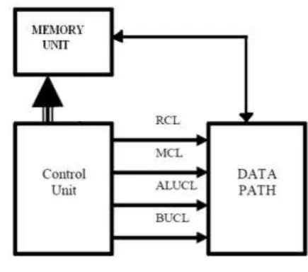
Control unitDatapath unit
[image:2.595.178.396.157.349.2]Memory unit
Figure 1. System Architecture
2.1 CONTOL UNIT:
The control unit design is based on using FSM(Finite State Machine) and designed it in way that allows each state to run at one clock cycle ,the first state is the reset which is initializes the CPU internal registers and variables. The machine
goes to reset state by enabling the reset signal for a certain number of clocks. Following the reset state would be the instruction fetching and decoding states which will enable the appropriate signals for reading instruction data from the ROM the decoding the part of the instruction. The decoding state will also select the next state depending on the instruction, every instruction has its own state .Based on the instruction ,the control unit select the appropriate state. After all operation for given instruction finished, the last state return to fetch state which will allow us to process the next instruction in the program.
2.2 DATAPATH UNIT
The datapath consist of subunits that are performing all of arithmetic and logic operations. It consist of the units necessary to perform all the operations on the data selected by the control unit. It consist of register file, ALU, memory interface and branching unit. A datapath is a hardware that performs data processing operations, the control lines coming from the control unit operate all the units in the datapath .The path starts from the register file that has two output ports which are connected to all other units, after that the processing is done by one of the other units then finally returned back to the register file input port using the multiplexer. The signals used in the datapath are forwarded from the control unit to each subcomponents needed.
2.3 MEMORY UNIT
The CPU has a built in ROM which enable us to program simple code and execute it. It is a basic 16*32 ROM and it is 32 bit aligned. The list of signals in the ROMare
Address -address sent by the control unity.
Data_out - data that is contained the given address.
Read - signal to enable reading from the ROM.
Ready - signal to indicate when the ROM is ready for reading.
© 2019, IRJET | Impact Factor value: 7.211 | ISO 9001:2008 Certified Journal | Page 3199
Reset - intial reset signal.3. SYSTEM DESIGN
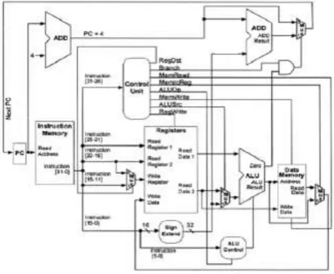
[image:3.595.177.421.196.396.2]The processor is based on the Harvard architecture that any instruction occupies separated positions of program memory and data memory(6)(7). Thus obtaining greater speed and a minor program length, also, the access time to the instructions can be superposed with one of the data, obtaining a greater speed in each operation(8). The processor includes a RISC instruction set and uses a Single Instruction – Single Data (SISD) execution order.
Figure 2. System Design
4. STAGES OF OPERATION
The overall diagram of the processor architecture s shown in figure 3. As seen from the diagram, the architecture(3) consists of a five stage of operations.
i. Instruction Fetch
ii. Instruction Decode
iii. Execute
iv. Memory
v. Write Back
Figure 3. Data Flow Diagram
4.1 INSTRUCTION FETCH
In this fetch cycle, the instructions are stored in the instruction memory, that instruction is to be fetched from the instruction memory. IR <= MEM[pc]
© 2019, IRJET | Impact Factor value: 7.211 | ISO 9001:2008 Certified Journal | Page 3200
This stage consists of three units.Program Counter, Instruction Memory and Branch Decide Unit.Figure 4. Block Diagram of Fetch Unit
4.2 INSTRUCTION DECODE
In this decode stage, instruction decode into operand codes, operand address information, control and the destination operand signal. This stage consists of four units Control Unit, Register Foley-Register and Sign Extend Unit.
Figure 5. Block Diagram Of Decode Unit
4.2.1 Control Unit:
[image:4.595.204.390.358.612.2]© 2019, IRJET | Impact Factor value: 7.211 | ISO 9001:2008 Certified Journal | Page 3201
Figure 6. Block Diagram of Control Unit4.3 EXECUTE
[image:5.595.225.372.100.235.2]In this execution stage(5), the data from decode stage is to be allowed for data processing operations. This stage consists of four modules: Branch Adder, Multiplier, Arithmetic Logic Unit and ALU Control Unit.
Figure 7. Block Diagram Of Execute Unit
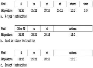
5. Instruction Set Architecture:
There are three basic types of instructions supported by this processor. Register Type, Branch Type and
Immediate Type.
The specification for each type of instructions is given below.
TABLE 1. Instruction Formats
[image:5.595.235.353.321.434.2] [image:5.595.205.390.583.717.2]© 2019, IRJET | Impact Factor value: 7.211 | ISO 9001:2008 Certified Journal | Page 3202
6. Simulation Results
Fetch Output
© 2019, IRJET | Impact Factor value: 7.211 | ISO 9001:2008 Certified Journal | Page 3203
CONTROL UNIT OUTPUT© 2019, IRJET | Impact Factor value: 7.211 | ISO 9001:2008 Certified Journal | Page 3204
7. CONCLUSION:
The design of 32-bit RISC processor has been presented.. Here we have used nearly twenty instructions . In that we have arithmetic operations, logical operations, shift operations and load & store operations. In our project, we implement only 8-bit Wallace tree multiplier and got output successfully. In future, it will enhance into 32-bit. By using MODELSIM 6.3f, the simulation results have been taken for all individual units successfully Most of the goals were achieved and simulation shows that the processor is working perfectly, but the Spartan 2E FPGA was not sufficient for implementing the whole design into a real hardware, since the total available logic gate in Spartan 3 Logic Gate, which was not
3.
REFERENCES
[1] W. Stallings, “organization and architecture of computer,” 7ªEditión, Pearson, 2006.
[2] M. Mano, “Architecture of computers,” 3ª Editión, Pearson, 1994.
[3] A.K.Ray, “Advanced Microprocessor And Peripherals”, 2nd Edition, Tata McGraw- Hill,2008
[4] D.V.Hall,“Microprocessor And Interfacing”, 2nd Edition, Tata McGraw-Hill,2006
[5] D. Mandalidis, P. Kenterlis, J. Ellinas, “A computer architecture educational system based on a 32-bit RISC processor,” International Review on computers and Software, pp. 114-119, 2008.
[6] Tocci, Widmer, Moss, “Sistemas Digitales, Principios y aplicaciones,” 10ª Editión, Pearson, 2007. Antonio H. Zavala, Jorge Avante R.,”RISC- Based Architecture for computer Hardware Introduction”.
[7] R. Uma, “Design and Performance Analysis of 8 – bit RISC Processor using Xilinx Tool”, International Journal of Engineering Research and Applications, Volume 2, Issue 2, March – April 2012, pp. 053 – 058, ISSN: 2248 – 9622.