Available online: https://edupediapublications.org/journals/index.php/IJR/ P a g e | 2089
Design of Pv System With Multilevel Structures for
Generation of Higher Number of Voltage Levels
Durga Prasad.V & A.Srikanth
1M.Tech (student), ST. Martin‟s Engineering College Affiliated to JNTUH, Hyderabad, Telangana, India.
Area of interest includes Power Electronics.
2Assistant Professor, ST. Martin‟s Engineering College Affiliated to JNTUH, Hyderabad, Telangana, India. Area of interest includes Power Electronics.
Abstract-A new method of generating higher number of voltage levels by stacking multilevel converters of lower space vector structures and having a single DC power supply as mentioned above with low voltage devices is presented in this paper. A photovoltaic system, also PV system or solar power system, is a power system designed to supply usable solar power by means of photovoltaics An important feature of this stacked structure is the use of low voltage devices while attaining higher number of levels. This will find extensive applications in electric vehicles since direct battery drive is possible. Stacked multi-cell converter was introduced to generate more levels. They use less number of capacitors but require more switches. Solar PV has specific advantages as an energy source: its operation generates no pollution and no greenhouse gas emissions once installed, The voltages of all the capacitors in the structure can be controlled within a switching cycle using the switching state redundancies (pole voltage redundancies). This helps in reducing the capacitor size. Also, the capacitor voltages can be balanced irrespective of modulation index and load power factor. A 9-level inverter is developed by stacking two 5-level inverters and an induction motor is run using V/f control scheme. By using the simulation results we can analyze the proposed method at both the steady state and transient state.
Index Terms—Active power control, constant power control, maximum power point tracking, PV systems, power converters.
INTRODUCTION
Photovoltaic (PV) power generation is becoming more promising since the introduction of the thin film PV technology due to its lower cost, excellent high temperature performance, low weight, flexibility, and glass-free easy installation. The multilevel inverter is more popular than a conventional two-level inverter, because the medium voltage rating power semiconductor devices may be employed for high power application along with higher power quality. In order to obtain better waveform quality and lower total harmonic distortion (THD) in the phase voltages, they also have advantages of reduced Electro-magnetic interference (EMI), lower device voltage ratings and lower switching frequency. Hence they found widespread applications in motor drives, grid tied converters, high voltage DC transmission, reactive power compensation, wind energy
conversion and in many other high power applications [2].Basic multilevel topologies include diode clamped multilevel inverter (DC-MLI), flying capacitor inverter (FC) and cascaded H-bridge inverter (CHB)[2],[3].Three level DCMLI, commonly known as neutral point clamped inverters (NPC) have become popular in industry. But for higher levels more clamping diodes are needed and also balancing the capacitors for entire modulation range is an issue [3]. To overcome the loss balancing problem, a modified version of NPC, known as the active NPC (ANPC) is introduced wherein the clamping diodes are replaced with the switches for balancing losses among the switches [5]. FCs are another class of MLCs where in several charged capacitors are used in generating higher number of voltage levels.
A photovoltaic system, also PV system or solar power system, is a power system designed to supply usable solar power by means of photovoltaics. It consists of an arrangement of several components, including solar panels to absorb and convert sunlight into electricity, a solar inverter to change the electric current from DC to AC, and mounting cabling and other electrical accessories to set up a working system.
Available online: https://edupediapublications.org/journals/index.php/IJR/ P a g e | 2090 output phase voltage waveform[1]. Multilevel
converters (MLC) are capable of generating higher levels in the output voltage waveform with low voltage stress on the switches.
This paper proposes a new method of generating higher number of levels in the voltage waveform by stacking multilevel converters with lower voltage space vector structures. Another breed of power converters are the CHB converters[2]. They have the least component count compared to DCMLIs and FCs especially due to absence of any clamping diodes or flying capacitors. But CHB based topologies reported with single DC supply and multiple floating capacitors in each phase are dependent on load power factor and modulation index for the floating capacitor balancing.
INVERTER TOPOLOGY AND ITS OPERATION
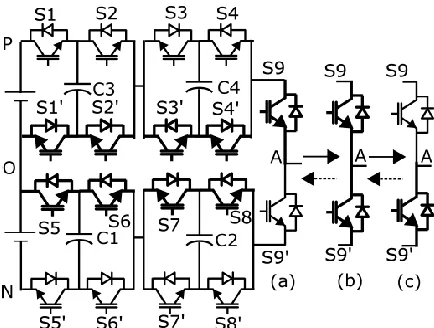
Each of the 5-level inverters are obtained by cascading a 3-level flying capacitor inverter and a capacitor fed H-bridge. There are 2 selector switches in each phase to connect the respective outputs to the induction machine.
The proposed inverter structure for a 9-level is shown in Fig. 1(a). It is realized by stacking two 5-level inverters in each phase.
Figure 1. Power circuit for the proposed stacked 9-level inverter and its modulating signal for phase „a‟.
(a) Proposed 9 level inverter by stacking two 5 level inverters
The flying capacitor in each structure has to be maintained at Vdc/4 and H bridge capacitors have to be maintained at Vdc/8, where Vdc is the DC link for a conventional 2-level inverter. The structure overall has 9 pairs of complimentary switches in each phase (S1-S1‟, S2-S2‟....S9-S9‟). Each of the switches in FC needs to block only Vdc/4 and each of the switches in H -bridge needs to block only Vdc/8.
During the positive half cycle of the reference waveform (signal-1 in Fig. 1(b)), the bottom structure is clamped to the mid point „O‟ by turning on S5, S6, S7, S8. Because of this operation,
the voltage rating of S9‟ has to be Vdc/2 only. The selector switches S9 is kept on and S9‟ is off during this period. Now the top structure will switch to generate the required pole voltages. Similarly during the negative half cycle (signal-2 in Fig. 1(b)), the top inverter structure is clamped to the mid point „O‟ by turning on S1‟, S2‟, S3‟, S4‟. S9‟ is kept on and S9 is permanently kept off. Again S9 has to be rated for only Vdc/2.
Figure 1. Power circuit for the proposed stacked 9-level inverter and its modulating signal for phase „a‟.
(b)Signal 1 for modulating the top structure and signal 2 for modulating the bottom structure along
with the 8 carriers
Here the bottom structure will switch to generate the required pole voltages. So the selector switches are switching at line frequency only. The selector switches switch only during the zero crossing of the modulating signal. When the modulating signal is transiting from positive half cycle to negative half cycle, the upper selector switch has to go off and bottom selector switch has to turn on. During this transition, it can be seen that all the top switches of the bottom structure (S5, S6, S7, S8) and all the bottom switches of the top structure (S1‟, S2‟ S3‟, S4‟) are on. If S9‟ is turned on just before S9 turns off, S9 can under go a zero voltage switching off. At the same time, S9‟ is undergoing a zero voltage switching on as shown in Fig. 2. The darkened switches in the figure are on.
Available online: https://edupediapublications.org/journals/index.php/IJR/ P a g e | 2091 modulating signal to eliminate switching loss in the
selector switches.
The solid arrow shows transition from positive to negative half cycle. The dotted arrow shows transition from negative to positive half cycle. All the darkened switches are on. Also this inverter has a modular structure, since the H bridges can be bypassed if it fails and the inverter can still operate in the entire modulation range with lower number of voltage levels.
CAPACITOR VOLTAGE BALANCING
The capacitor voltages need to be maintained at the respective levels for generating the pole voltages. Each of the capacitor voltages in the topology has to be maintained at their reference values. Hence we define a small hysteresis band for each of the capacitor voltage references and maintains the voltages within this band using the available switching state redundancies. During a sampling instant, if the capacitor charges and reaches the upper limit of the hysteresis band, immediately in the next sampling instant, the switching state is changed to discharge that capacitor. Since the capacitors are designed considering the switching frequency, peak of load current and the voltage deviation, the capacitor voltages always lie within the hysteresis band.
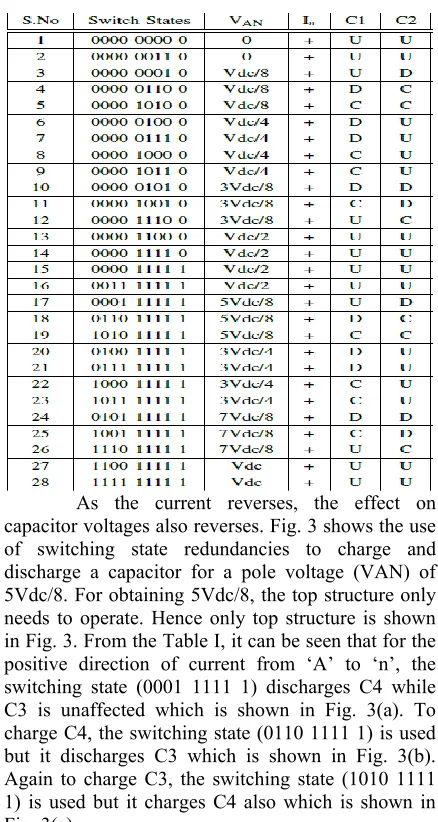
Table I list all the switching redundancies of all the pole voltages and also their effect on the capacitor voltages for a particular direction of current.
Table I
SWITCHING STATE REDUNDANCIES FOR THE POLE VOLTAGES AND THEIR EFFECT ON THE
CAPACITOR VOLTAGES.
Available online: https://edupediapublications.org/journals/index.php/IJR/ P a g e | 2092 Figure 3. Switching redundancies available for a pole
voltage. (a), (b) and (c) show current paths and charge and discharge of capacitors for switching redundancies available for pole voltage of 5Vdc/8
Whenever the capacitor voltages crosses the hysteresis limits, switching states need to change to maintain the capacitor voltages to desired values. For pole voltages of 0, Vdc/2 and Vdc, none of the capacitors are affected due to the current flow. For all other pole voltages, capacitor voltages change with current flow
Again the application of switching state depends on the present state of capacitor voltages and the current directions. Hence all the 12 capacitor voltages and currents are sensed. All the capacitor voltages are compared with their references and capacitor voltage status whether it has exceeded the upper or lower limit of the hysteresis band is given by Hax, where x = 1,2,3,4 respectively for C1, C2, C3 and C4. Hax = „1‟ implies capacitor needs discharging and Hax = „0‟ implies capacitor needs charging to maintain the capacitor voltages within the hysteresis band. Capacitor voltage status, the required pole voltage and the current direction decide the switching state at any instant.
Table II tells which switching state needs to be applied at any instant depending on the above factors. Thus instantaneous capacitor voltage control using switch state redundancies are possible within inverter switching cycle. This is also independent of load power factor.
Table II
SWITCHING STATE SELECTION TABLE BASED ON CURRENT DIRECTION AND CAPACITOR VOLTAGE STATUS FOR PHASE „A‟
GENERALIZATION
In the proposed 9-level inverter shown in Fig. 1(a), two 5-level inverters are stacked and each 5-level inverter is generating half of the total inverter pole voltage. During the positive half cycle of the reference modulating signal (trace-2 of of Fig. 11), the top selector switch is on and during the negative half cycle, the bottom selector switch is on, to connect the respective 5-level stacked inverter modules to the output. The gate signal to the top
selector switch is shown in trace-3 of Fig 11.To reduce the number of switches, the structure in Fig. 1(a) can be modified as shown in
COMPARISON WITH OTHER INVERTER TOPOLOGIES
Available online: https://edupediapublications.org/journals/index.php/IJR/ P a g e | 2093 Figure 4. Modified power circuit to reduce number of
switches for the proposed stacked 9-level inverter topology for phase „a‟.
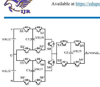
Fig. 4. Here the H bridge is made common to both the FC and selector switch is connected in between. Here the H-bridge switches need to switch throughout the cycle. But they need to block voltage of Vdc/8 only (same as that in Fig. 1(a)). Therefore the switching losses are controlled. Also by using redundant H-bridges, the system reliability can be improved. This method of stacking can be extended to obtain higher voltage levels.
The modified proposed topology requires total of 42 switches. Out of which, six selector switches are switching at line frequency and whose switching losses can be minimized using the method discussed in the earlier section. The top and bottom FC is operating only for one half of a fundamental cycle and is idle during the other half. In the conventional NPC and FC topologies for 9-level, many clamping diodes and flying capacitors are required for their operation respectively. In the proposed structure with less number of floating capacitors, capacitor balancing can be done throughout the modulation range irrespective of any load power factor, whereas in a 9-level NPC, there is a limitation on modulation index due to the capacitor unbalance problem.
In Fig. 5, a 49-level inverter is shown which is developed by stacking 3 FC and cascading with 3 capacitor fed H-bridges (which are of lower voltage ratings) through a 3-level selector switch. It is shown that a FC cascaded with 3 H-bridges can generate 17 levels. Since there are 3 stacked 17-level inverters, the reference signal has to be divided into three parts
and each will be used for modulating each of the 17-level inverter formed by cascading 3 capacitor fed H-bridges with a FC. Also due to the higher number of voltage levels, switching frequency can be reduced and therefore higher efficiency is achievable. These advantages will make the stacked inverter structure suitable for application in electric vehicles where the inverter can be driven directly from the stacked low voltage batteries.
Figure 5. Power circuit schematic for generation of 49 levels by stacking three FC and cascading with three capacitor fed H-bridges of low voltage ratings
Available online: https://edupediapublications.org/journals/index.php/IJR/ P a g e | 2094 Table III
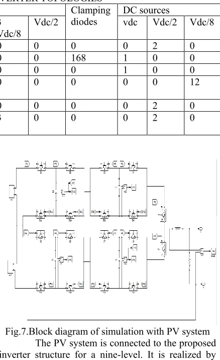
COMPARISON OF 9-LEVEL INVERTER TOPOLOGIES
Topolgies IGBT capacitors Clamping
diodes
DC sources Vdc/2 Vdc/4 Vdc/8 Vdc/4 Vdc/8 3
Vdc/8
Vdc/2 vdc Vdc/2 Vdc/8
proposed 6 24 12 6 3 0 0 0 0 2 0
NPC 0 0 48 0 8 0 0 168 1 0 0
FC 0 0 48 0 84 0 0 0 1 0 0
Conventional
CHB 0 0 48 0 0 0 0 0 0 0 12
Open end 9L 12 12 12 0 9 0 0 0 0 2 0
Standard
9L-ANPC 12 0 24 3 3 3 0 0 0 2 0
PV SOURCE
Photovoltaics (PV) covers the conversion of light into electricity using semiconducting materials that exhibit the photovoltaic effect, a phenomenon studied in physics, photochemistry, and electrochemistry. The dynamic model of PV cell is shown in below Fig.6.
Fig 6.Equivalent electrical circuit of the PV cell. The basic equation describing the I -V characteristic of a practical PV cell is
I = IL− Id− Ish = IL− ID e
Q V oc
AKT −1 −Vout+IRS
RSh (1) where I D is the saturation current of the diode, Q is the electron charge, A is the curve fitting constant (or diode emission factor), K is the Boltzmann constant and T is the temperature on absolute scale. PV systems convert light directly into electricity and shouldn't be confused with other technologies, such as concentrated solar power or solar thermal, used for heating and cooling.
Photovoltaics (PV) is a term which covers the conversion of light into electricity that exhibit the photovoltaic effect, a phenomenon studied in physics, photochemistry, and electrochemistry. Photovoltaic (PV) power generation is becoming more promising since the introduction of the thin film PV technology due to its lower cost, excellent high temperature performance, low weight, flexibility, and glass-free easy installation.
Fig.7.Block diagram of simulation with PV system The PV system is connected to the proposed inverter structure for a nine-level. It is realized by stacking two five-level inverters in each phase.
Fig.8.Simulation diagram of PV system
SIMULATION RESULTS
A 3 phase, 415V, 7.5KW, 50 Hz induction motor (IM) is driven with the proposed 9-level inverter shown in Fig. 1(a) using open loop V/f control scheme.
Available online: https://edupediapublications.org/journals/index.php/IJR/ P a g e | 2095 PWM technique is implemented for the proposed
inverter.
(a)
(b)
(c)
(d)
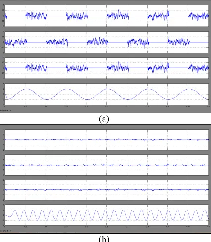
Figure 9. Motor Phase voltage (VAn), Inverter pole voltage (VAO), Capacitor voltage ripple (Vc3),
Phase current (Ia) for phase A for different modulation indices. (b), (c) and (d) y-axis 1) VAn: 100V/div, 2) VAO: 100V/div 3) Vc3: 5V/div 4) Ia:
2A/div. (a) y-axis 1) VAn: 50V/div, 2) VAO: 50V/div 3) Vc3: 5V/div 4) Ia: 2A/div
The results showing the inverter phase voltages (trace-1), pole voltages with respect to midpoint „O‟ (trace-2), the flying capacitor voltage ripple of top structure (trace-3) and phase current (trace-4) for „a‟ phase are shown for 10 Hz operation (Fig. 7(a)), 20 Hz operation (Fig. 7(b)), 30 Hz operation (Fig. 7(c)) and 45 Hz operation (Fig. 7(d)).
(a)
(b)
Figure 10. Capacitor voltages ripple and motor phase current for „a‟ phase. y-axis: 1) ∆Vc1: 5V/div, 2)
Available online: https://edupediapublications.org/journals/index.php/IJR/ P a g e | 2096 It can be seen in the above figures that as the
speed command is increased from 10 Hz to 45 Hz, the number of levels in the pole voltage waveform (trace-2) increases from 3 to 9.
(a)
(b)
Figure 11. (a) Motor acceleration. (b) Intentional capacitor unbalancing. yaxes: 1) Motor Phase voltage
(VAn), 2) Capacitor voltage Vc4, 3) Capacitor voltage Vc3, 4) Phase current (Ia).
To test the capacitor voltage balancing algorithm, the balancing algorithm is intentionally disabled at Td and then enabled at Te as shown in Fig. 12(b).
(a)
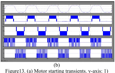
(b)
Figure13. (a) Motor starting transients. y-axis: 1) Motor Phase voltage (VAn), 2) Capacitor voltage Vc3, 3) Capacitor voltage Vc4, 4) Phase current (Ia).
(b) Individual FC pole voltages (traces-2,3) and Individual H-bridge switchings (traces-4,5). 1) Modulating signal, 2) VWO, 100V/div, 3) VYO,
100V/div, 4) VXW, 20V/div, 5) VZY, 50V/div.
Figure 14. Modulating signals and the generated pole voltages by each of the stacked cells and the inverter
at 45 Hz operation. x axis: 10ms/div. 2) VAO, 100V/div, 3) Gating signal, 50V/div, 5) VXO,
100V/div, 7) VZO, 100V/div.
CONCLUSION
H-Available online: https://edupediapublications.org/journals/index.php/IJR/ P a g e | 2097 bridges. The concept of stacking can be generalized
to obtain higher voltage levels. As the number of levels increases, blocking voltages of switches reduces and the proposed structure can be fed from low voltage battery cells. Also, higher number of voltage levels imply lower switching frequency and therefore higher efficiency, which makes it suitable for application in electric vehicles. Hysteresis based capacitor voltage balancing algorithm is used to maintain the capacitor voltages irrespective of modulation index and load power factor. By using the simulation results we can analyze the proposed method.
REFERENCES
[1] A. Nabae, I. Takahashi, and H. Akagi, “A new neutral-point-clamped PWM inverter,” IEEE Trans. Ind. Appl., vol. IA-17, no. 5, pp. 518–523, Sept 1981. [2] S. Kouro, M. Malinowski, K. Gopakumar, J. Pou, L. Franquelo, B. Wu, J. Rodriguez, M. Perez, and J. Leon, “Recent advances and industrial applications of multilevel converters,” IEEE Trans. Ind. Electron., vol. 57, no. 8, pp. 2553–2580, Aug 2010.
[3] J. Rodriguez, S. Bernet, P. Steimer, and I. Lizama, “A survey on neutralpoint- clamped inverters,” IEEE Trans. Ind. Electron., vol. 57, no. 7, pp. 2219–2230, July 2010.
[4] P. Barbosa, P. Steimer, J. Steinke, L. Meysenc, M. Winkelnkemper, and N. Celanovic, “Active neutral-point-clamped multilevel converters,” in Proc. 2005 IEEE Power Electron. Special. Conf., June 2005, pp. 2296– 2301.
[5] T. Bruckner, S. Bernet, and H. Guldner, “The active npc converter and its loss-balancing control,” IEEE Trans. Ind. Electron., vol. 52, no. 3, pp. 855– 868, June 2005.
[6] H. Wang and F. Blaabjerg, “Reliability of capacitors for dc-link applications in power electronic converters ;an overview,” IEEE Trans. Ind. Appl., vol. 50, no. 5, pp. 3569–3578, Sept 2014. [7] S. Pulikanti and V. Agelidis, “Hybrid flying-capacitor-based activeneutral- point-clamped five-level converter operated with SHE-PWM,” IEEE Trans. Ind. Electron., vol. 58, no. 10, pp. 4643–4653, Oct 2011.
[8] T. Chaudhuri, P. Steimer, and A. Rufer, “Introducing the common cross connected stage (c3s) for the 5l ANPC multilevel inverter,” in Proc. IEEE Power Electron. Special. Conf., June 2008, pp. 167– 173
[9] P. Rajeevan, K. Sivakumar, K. Gopakumar, C. Patel, and H. Abu-Rub, “A nine-level inverter topology for medium-voltage induction motor drive
with open-end stator winding,” IEEE Trans. Ind. Electron., vol. 60, no. 9, pp. 3627–3636, Sept 2013.
DURGA PRASAD .V
Completed B.Tech in Electrical & Electronics Engineering in 2014 from S.S Institute of Technology Affiliated to JNTUH, Hyderabad and Pursuing M.Tech form ST. Martin‟s Engineering College Affiliated to JNTUH, Hyderabad, Telangana, India. Area of interest includes Power Electronics.
E-mail id:[email protected]
A.SRIKANTH
Completed B.Tech in Electrical &Electronics Engineering in 2010 fromST. Martin‟s Engineering College Affiliated to JNTUH, Hyderabad and M.Tech in Elecrtical Power Systems in 2013from ST. Martin‟s Engineering College Affiliated to JNTUH, Hyderabad. Working as Assistant Professor at ST. Martin‟s Engineering College, Kompally, Hyderabad, Telangana, India. Area of interest includes Electrical Power System, power electronic.