© 2017, IRJET | Impact Factor value: 5.181 | ISO 9001:2008 Certified Journal
| Page 131
Performance Analysis of Reversible 16 Bit ALU based on Novel
Programmable Reversible Logic Gate Structures
Sanjay Kumar
1, Dr.Harjinder Singh
21
M.Tech. Scholar, Department of Electronics and Communication Engineering, Punjabi University Patiala
2Assistant Professor, Department of Electronics and Communication Engineering, Punjabi University Patiala
---***---
Abstract -
Reversible logic is promising as it is able tocompute with various applications in very low power like nano-computing for example quantum computing. Reversible circuits are like conventional circuits despite these are build from reversible gates. Reversible circuits, have single, one-to-one mapping between the input and output vectors. Conventional digital circuits dissipate a significant amount of energy because bits of information are erased during the logic operations. Reversible logic units are required to recover the state of inputs from its outputs. Low power is challenging work in processor design. One of the most basic operational units in the processor is an Arithmetic and Logical Unit (ALU). Arithmetic and Logical Unit (ALU) is a critical component of a microprocessor and is the core component of central processing unit. This paper describes the design technique for low power, low area Arithmetic and Logical Unit (ALU) design. Reversible logic is special optimization technique having its application in low power design. Simulation of circuits is done by ISE Simulator and language used for programming is very high speed hardware integrated circuit hardware descriptive language (Verilog).
Keywords: Reversible logic gates, Fredkin gate, Toffoli Gate, Hagparast Navi Gate (HNG).
1. INTRODUCTION
Since the demand for more compact system designs with portability and higher speed is increasing, the need for improving the capabilities of these entities has been a major research area for example, in hand held devices. These devices must also operate at low power levels. Landauer proved that using irreversible logic gates always lead to energy dissipation regardless of the underlying technology. Exactly, KT*ln2 Joule of energy is dissipated for each “lost” bit of information during the irreversible operation (where K=1.38*10-23 JK-1 is the Boltzmann constant and T is the temperature in
Kelvin)[1]. C. H. Bennett showed that energy dissipation problem can be avoided if circuits are built using reversible logic gates [2]. For this to be true, the circuit should be both physically and logically reversible. Practically, there will be power dissipation less than the KT*ln2 limit in CMOS irreversible circuits. A gate realizing a certain reversible logic function is called a reversible logic gate. A circuit made by concatenating these gates is called a reversible logic circuit. An irreversible logic gate can also be expressed in terms of reversible gates and such circuits can be synthesized with minimum energy consumption or zero entropy gain [3]. Due to the one to one mapping between input and output, the power dissipation is very small in the reversible circuits. Thus, reversible designs are gaining wide importance in the fields of quantum computing, nanotechnology, low power CMOS design and other advanced applications. The goals of reversible logic design are mainly to minimize the quantum cost, delay as well as the ancillary inputs and garbage outputs. From the above discussion it is clear that reversible logic is the upcoming field in low power technology. The reversible logic is, therefore, being used for the design of the ALUs. This paper proposed the design of reversible 16 bit Arithmetic and Logical Unit (ALU).
2. REVERSIBLE LOGIC GATES
In the existing literature, there are several numbers of reversible gates such as the Feynman gate and Fredkin gate. The quantum cost of any circuit depends on number of 1x1 and 2x2 reversible gates needed to design that circuit. The quantum cost of all 1x1 and 2x2 reversible gates are considered as unity. The 1x1 NOT gate and 2x2 reversible gates are use
© 2017, IRJET | Impact Factor value: 5.181 | ISO 9001:2008 Certified Journal
| Page 132
Feynman gate also known as Controlled -NOT gate (CNOT).
2.1 NOT Gate
[image:2.595.50.263.205.289.2]A NOT gate is 1x1 gate represented as shown in Fig -1. Since it is a 1x1 gate, its quantum cost is unity.
Fig -1: Not Gate
Not gate as shown above can be used as control gate and this gate have zero quantum costs as this have only one input and one output so same in irreversible and reversible.
2.2 Fredkin Gate
[image:2.595.337.541.354.525.2]Fredkin gate is a 3x3 reversible logic gate with three inputs and three outputs.
Fig - 2: Fredkin gate
Fig -2 shows the block diagram of a Fredkin gate. Fredkin gate, maps the inputs A, B, and C to outputs as P=A, Q = A¯B + AC, and R = AB + A¯C respectively. A Fredkin gate can work as 2:1 MUX, as it is able to swap its other two inputs depending on the value of its first input. Referring the Fig -2, the first input A works as a controlling input, while the both B and C work as controlled inputs. Thus, when A=1 the inputs B and C will give outputs as Q=C and R=B and thus input gets swapped. If A=0 the inputs B and C will give outputs as Q=B and R=C.
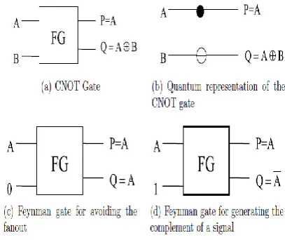
2.3 Feynman Gate (CNOT Gate)
[image:2.595.51.268.430.545.2]The Feynman gate (FG) or the controlled-NOT gate (CNOT) is a 2x2 reversible gate. The inputs A and B are mapped to outputs as P=A and Q=A⊕B respectively. Here, A is the controlling input and B is the controlled input whereas P and Q are the two outputs. Since the Feynman gate is a 2x2 reversible gate, it has a quantum cost of 1. Fig -3(a) and 3(b) shows the block diagram the quantum representation of the Feynman gate. Each output in reversible logic can be used only once so fan out is not allowed. Feynman gate is helpful in this regard as same output can be generated on both output terminals at same time, thus avoiding the fan-out problem as shown in Fig -3(c). It can also be used for generating the complement of a given input signal as shown inFig -3(d).
Fig -3: CNOT gate, its quantum implementation and its useful properties
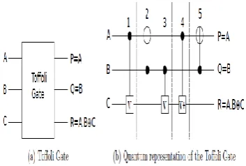
2.4 Toffoli Gate
The Toffoli gate (TG) is a 3x3 reversible logic gate with three inputs and three outputs. The input of Toffoli gate as A ,B and C are mapped to P = A, Q = B and R = ((A B)⊕
C) respectively.
© 2017, IRJET | Impact Factor value: 5.181 | ISO 9001:2008 Certified Journal
| Page 133
Fig -4: Toffoli Gate and its quantum implementation
2.5 HNG Gate
The Hagparast Navi (HNG) gate is a 4x4 reversible logic gate with three inputs and three outputs as shown in Fig -5. The inputs of HNG gate as A, B, C and D are mapped to P = A, Q = B, R = (A ⊕B⊕C) and S = (A⊕B) C⊕AB⊕D respectively. The reversible HNG gate can work singly as a reversible full adder. If the input vector IV = (A, B, Cin, 0), then the output vector becomes OV = (P=A, Q=Cin, R=Sum, S=Cout).
Fig -5: Hagparast Navi (HNG) gate
3. PROPSED MODEL OF REVERSIBLE ALU
[image:3.595.324.548.368.553.2]The proposed model of Reversible Arithmetic and Logical Unit (ALU) consist of Arithmetic Unit, Logic Unit and 2:1 MUX as shown in Fig -6.
Fig -6: Proposed Reversible ALU Model
3.1 One bit Arithmetic Unit
[image:3.595.46.264.431.566.2]One bit purposed structure of Arithmetic unit is as shown in Fig -7 composed of two Double Feynman gate, one Feynman gate, one Fredkin gate and one HNG gate.
Fig -7: One bit Arithmetic Unit
HNG gate is used as full adder and two Double Feynman gate, one Feynman gate with one Fredkin gate provide the control mechanism which gives various arithmetic functions. A, B and Cin represents the input signals and Sum, Cout represents the output signals. S0 and S1 are the select lines signals. The single arithmetic unit has five ancilla inputs and three garbage outputs. The Boolean equation for the Arithmetic unit is:-
Sum = A ⊕ Y1 ⊕ Cin Cout = AY1 ⊕ Y1 Cin ⊕ ACin
For HNG gate we have three inputs i.e. A, Y1 and Cin so equation for Y1 is as follows:
© 2017, IRJET | Impact Factor value: 5.181 | ISO 9001:2008 Certified Journal
| Page 134
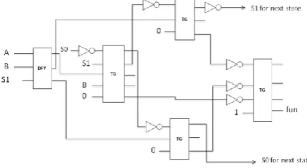
3.2 One bit Logical Unit
[image:4.595.39.258.278.398.2]One bit Logical Unit is composed of one 4*4 Toffoli gate , two 3*3 and one 5*5 Toffoli gates and one Double Feynman gate as shown in Fig -8 to performs four basic logic operations viz. AND , OR , XOR and NOT. A, B represents the input signals and fun represents the output signal. S0 and S1 are the select lines signals. The Boolean equation for the logic unit is Y = S1 (A⊕B) +S0S1AB +S0 (A⊕S1). This reversible logic unit has four ancilla inputs and five garbage output. It provides great reduction in the logic power in comparison to the irreversible logic unit.
Fig -8: One bit Logical Unit
3.3 Reversible MUX Design
2:1 MUX is used for combining the two unit viz. Arithmetic and Logical Unit together. Here MUX is realized using three Toffoli gates as shown in Fig -9. MUX equation is OUT = A.S + B.S. This MUX provide significant reduction in the power in comparison to irreversible MUX. It is used for multiplexing the Arithmetic unit and Logical unit for making single unit i.e. Arithmetic and Logical Unit. Sum and fun are the input signals from Arithmetic unit and Logic unit respectively. The input M represents the mode selector input and Fun is the output signal. This reversible MUX have three ancilla inputs and five garbage outputs.
Fig -9: Reversible MUX Design
3.4 16-bit Arithmetic Unit
16 bit purposed structure of Arithmetic Unit is obtained from single bit structure by propagating both select lines S0,S1 and carry output to the next stage. The purposed 16 bit arithmetic unit have 80 number of ancilla inputs and 48 number of garbage outputs. In the same way N bit arithmetic unit can be obtained as 16 bit arithmetic unit and have 5N ancilla inputs and 3N garbage outputs.
3.5 16-bit Logical Unit
16 bit structure of the logic unit can be obtained from the single bit reversible purposed structure by propagating the select lines S0 and S1. For this 16 bit logic unit the number of ancilla inputs and garbage outputs will be 64 and 80 respectively. Total number of gates for 16 bits will be 192. In the same way N bit logic unit can be obtained as 16 bit logic unit and have 4N ancilla inputs i.e. constant inputs and 5N garbage outputs. Total number of gates used for this design is 12 N.
4. RESULT AND DISCUSSIONS
4.1 Simulation
[image:4.595.315.562.562.714.2]The functional correctness of our reversible Arithmetic and Logical Unit (ALU) is verified with the use of ISE simulator to make the corresponding simulation. A and B are two 16 bit inputs and M, S0, S1 are select lines. Fun is the 16 bit output. Fig -10 shows the simulation of 16 bit reversible Arithmetic and Logical Unit (ALU). Post synthesis simulation is also done which is same as the pre synthesis simulation.
© 2017, IRJET | Impact Factor value: 5.181 | ISO 9001:2008 Certified Journal
| Page 135
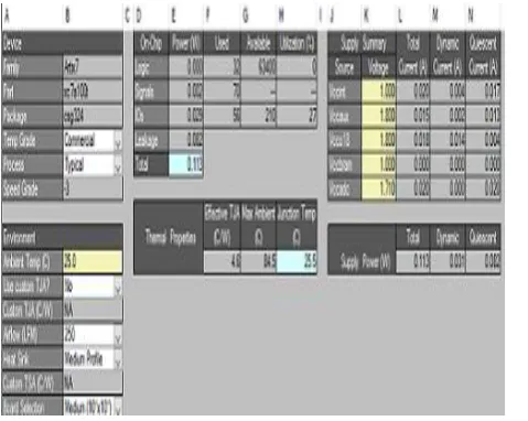
4.2 Power analysis
The Xilinx Power Analyzer can perform a power analysis at any time during the design cycle. Signal rate play a significant role in the power calculation it is defined as how many times that particular signal changes during clock period. It is very critical for the designer to provide this for efficient power calculation. Reversible logic structures reduce the dynamic power consumption especially magical reduction in the logic power. The important power components to consider include the following:
Static (standby) power
Static power is the amount of power the device consumes when it is powered-up but not actively performing any operation (i.e. the device is not clocked).
Dynamic (active) power
Dynamic power is the amount of power the device consumes when it is actively operating (i.e. the device is clocked). Total power for the 16 bit reversible Arithmetic Logical Unit (ALU) is the sum of device static power i.e. leakage power and dynamic power. Dynamic power is the sum of input/output power, logic power and data power which shown in Fig -11. It is reduced by 5.12 % in comparison to irreversible Arithmetic Logical Unit (ALU).
Fig -11: Power dissipation for 16 bit reversible Arithmetic and Logical Unit (ALU)
Input/ Output power
This is the power dissipation when the device is conFigd but there is no switching activity. The input/output power for 16 bit reversible Arithmetic and Logical Unit (ALU) is 28.86 mW whereas input/output power for 16 bit irreversible Arithmetic and Logical Unit (ALU) is 37 mW.
Data Power
Data power dissipation is due to the data switching. It is reduced by 34.78 % through reversible logic gates in comparison to 16 bit irreversible Arithmetic and Logical Unit (ALU) which perform the same functionality. Data power for the 16 bit reversible Arithmetic and Logical Unit (ALU) is 1.5 mW.
Logic Power
[image:5.595.43.283.518.709.2]
Logic power is the additional power consumption from the user logic utilization and switching activity also called design dynamic power. There is magical reduction in the logic power consumption using reversible logic gates because of one to one correspondence between input and output which prevent the loss of bits. Logic power consumption is reduced by 53.3 % for 16 bit reversible Arithmetic and Logical Unit (ALU) as shown in the Table -1.
Table -1: Power dissipation comparison for 16 bit Arithmetic and Logical Unit (ALU)
Source of power
16 Bit Irreversible ALU ( mW )
16 Bit Reversible ALU ( mW )
Logic Power
.75 .35
Data Power
2.3 1.5
I/O Power 37 28.86
Total Power
© 2017, IRJET | Impact Factor value: 5.181 | ISO 9001:2008 Certified Journal
| Page 136
Area comparison for Arithmetic and Logical Unit(ALU)
[image:6.595.46.271.245.375.2]Table -2 shows the area comparison between irreversible and reversible Arithmetic and Logical Unit (ALU). The Area is reduced by 33.33% by using reversible Arithmetic and Logical Unit.
Table -2: Area comparison of 16 bit Arithmetic and Logical Unit (ALU)
Parameters 16 Bit
Irreversible ALU
16 Bit Reversible
ALU
No. of Slice LUTs
48 32
No. of
Occupied Slices
22 19
No. of LUT flip- flop pair used
[image:6.595.45.273.425.649.2]48 32
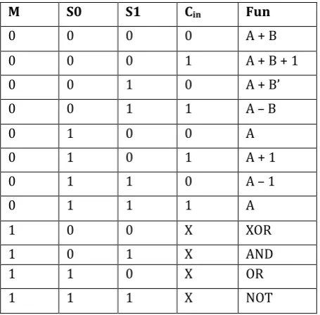
Table -3: Functional table for Arithmetic and Logical Unit (ALU)
M S0 S1 Cin Fun
0 0 0 0 A + B
0 0 0 1 A + B + 1
0 0 1 0 A + B’
0 0 1 1 A – B
0 1 0 0 A
0 1 0 1 A + 1
0 1 1 0 A – 1
0 1 1 1 A
1 0 0 X XOR
1 0 1 X AND
1 1 0 X OR
1 1 1 X NOT
5. CONCLUSION AND FUTURE SCOPE
The new reversible Arithmetic and Logical Unit (ALU) designs are advantageous to irreversible Arithmetic and Logical Unit (ALU) and favor low power dissipation and also consume less area which is desirable for realization
of a reversible central processing unit. RTL coding is done in Verilog HDL and simulation is done with ISE Simulator. Synthesis is done with Xilinx 14.7. Power is estimated using XPower analyzers from which it is estimated the logic power and area is reduced by 53.3% and 33.33% respectively. The results of the research can be exploited very effectively in quantum computing and low power design. The future scope of this research includes the applicability of Moore's law in the next few decades through the quantum computing using reversible logic. This reversible Arithmetic and Logical Unit (ALU) can be used in applications such as quantum computing, nanotechnology, optical computing, low power VLSI designs etc. The extended operations will be more useful for doing complex logic designs. Many ASICs based projects could be possible by using the proposed reversible Arithmetic and Logical Unit (ALU) design.
REFERENCES
[1] Priyal Grover and Hemant Verma, “Design, Layout and Simulation of 8 bit Arithmetic and Logical Unit” International Journal of Electrical and Electronics Engineers (IEEE),Vol. 07, Issue 02, July- December 2015.
[2] Shefali Mamtaj, Biswajit Das, Anurima Rahama “An Optimized Realization of ALU for 12 Operation by using a Control Unit of Reversible Gates”, International Journal of Advanced Research in Computer Science and Software Engineering (IJARCSSE), Vol. 04, Issue 01, January 2014.
[3] Ajay Kumar Sharma and Anshul Jain, “Design of Low Power Low Area Arithmetic and Logical Unit” International Journal of Innovative Research in Computer and Communication Engineering (IJIRCCE), Vol. 02, Issue 12, December 2014.
[4] Chetan Kumar, Dr. Rekha.K .R and Dr. Natraj K .R, “Implementation of 16 bit Arithmetic and Logical Unit using Toffoli Reversible Logic Gate” International Journal of Innovative Science, Engineering and Technology (IJISET), Vol. 01, Issue 06, August 2014.
© 2017, IRJET | Impact Factor value: 5.181 | ISO 9001:2008 Certified Journal
| Page 137
[6] Akanksha Dixit and Vinod Kapse, “Arithmetic and Logical Unit Design using Reversible Control Unit”, International Journal of Engineering and Innovative Technology (IJEIT), Vol. 01, Issue 06, June 2012.
[7] Zhijin Guan, Wenjuan Li, Weiping Ding, Yueqin Hang and Lihui Ni, “An Arithmetic and Logical Unit Design based on Reversible Logic Gates”, International Journal of Electrical and Electronics Engineers (IEEE), 2011.
[8] Avinash G. Keskar and Vishal R. Satpute, “Design of 8 bit Novel Reversible Arithmetic and Logical Unit” International Journal of Electrical and Electronics Engineers (IEEE),2011.
[9] Y.Syamala and A. V. N. Tilak, “Reversible Arithmetic and Logical Unit” International Journal of Electrical and Electronics Engineers (IEEE), 2011.
[10] R.Landauer, “Irreversibility and Heat Generation in the Computational Process”, IBM Journal of Research and Development, Vol. 05, 1961.
[11] C.H. Bennett, “Notes on the History of Reversible
Computation”, IBM Journal of Research and
Development, Vol. 32, 1998.
[12] Monika Rangari, Prof. Richa Saraswat and Dr. Rita Jain, “Design of Reversible Logic ALU using Reversible logic gates with Low Delay Profile” International Journal of Advanced Research in Computer and Communication Engineering, Vol. 04, Issue 4, April 2015.
[13] Ravi Raj Singh, Sapna Upadhyay, Saranya S, Soumya, Jagannath KB and Hariprasad SA, “Efficient Design of Arithmetic and Logical Unit using Reversible Logic Gates” International Journal of Advanced Research in Computer Engineering & Technology (IJARCET), Vol. 3, Issue 4, April 2014.
[14] Darshan H, Mohanraj R, Kavya H B, Monisha U K and Saroja Maralabhavi, “Design and Synthesis of 8 Bit Reversible Arithmetic & Logical Unit (ALU)” ITSI Transactions on Electrical and Electronics Engineering (ITSI-TEEE), Vol. 3, Issue 03, 2015.
[15] Khushboo Ahirwar, Sachin Bandewar and Anand Kumar Singh, “FPGA Implementation ALU Based on Reversible Logic” International Journal of Engineering
Research & Technology (IJERT), Vol. 3 Issue 1, January 2014.
[16] Pradeep singla and Naveen Kr. Malik, “ A Cost Effective Design of Reversible programmable logic array” International Journal Of Computer Application, Vol. 41, March 2012.