DESIGN OF LOW POWER DISCRETE TIME SIGMA-DELTA
MODULATOR FOR ANALOG TO DIGITAL CONVERTER
RADHOUANE LAAJIMI
Department of Electrical Engineering,
Electronics Micro-technology and Communication (EMC) research group Sfax (ENIS), BP W, 3038 Sfax, Tunisia
E-mail: [email protected]
ABSTRACT
Modulator is one of the most significant building-blocks in integrated discrete time component used in Sigma-Delta (ΣΔ) analog to digital converter. In this paper a novel structure of a switched-capacitor discrete time first order modulator Sigma-Delta is implemented at a supply voltage of 3 V. In addition, our design uses a Miller operational transconductance amplifier topology for low power consumption. The designed modulator has a resolution of 8 bits at a sampling frequency of 10.24 MHz. Eventually the modulator consumes only 1.16 mW of power under 3V. The core chip size of the modulator without bonding pads is 0.008 mm2 (76 µm x 110 µm) by using the AMS 0.35 µm CMOS technology.
Keywords: Sigma-Delta modulation, CMOS technology, switched-capacitor circuits, Analog-to-digital
(ADC), Analog circuit design.
1. INTRODUCTION
L
ow power consumption is not always a result oflow supply voltages. The additional signal processing required to maintain the same or maybe an even better dynamic range despite the reduction in supply voltage, may cause additional power consumption. For example ΣΔ analog to digital converter (ADC) [1] needs a low supply voltage between 0.5 and 0.6 V, which is sufficient to be embedded between 45 and 65 nm. The problem of this ΣΔ ADC is how to conserve the same dynamic range at a supply voltage of 1.8 V. In order to resolve this problem, the using of switched capacitors filters for the noise shaping is necessary. Rather than use switches, the operational can be switched themselves.
In literature many types of ADC are proposed. Such as a successive approximation ADC [2]. This last uses a switched current to provide a resolution of 12 bits at a sampling frequency of 1.7 MHz, with current draw of 4mA, in 0.25 µm CMOS technology. Another type of ADC based on a redundant signed-digit cyclic algorithm [3]. This design achieves a resolution of 12 bits at a sampling frequency of 1.7 MHz, with current draw of 1.8mA in 0.35 CMOS technology. According to successive approximation converter, the redundant signed-digit consumes only half the power. A low power ADC
based on second order Sigma- Delta modulator [4], was designed to achieve a resolution of 16 bits at a sampling frequency of 12.8 MHz and a current draw of 2.76 mA. This design has a higher performance much greater than the previous designs due to the high output resolution of 16 bits. Another same architecture of low power approach used for third order ΣΔ design [5]. It achieves a resolution of 10 bits, at a sampling frequency of 500 KHz, with current draw of 67 µA in 0.7 µm CMOS technology. According to the previous designs, this design illustrates a good example for the trade-off between performance and power consumption.
An incoming analog signal is sampled at very higher frequency by a ΣΔ [6] converter. According to the Nyquist, the minimum sampling frequency is twice the maximum frequency of the incoming signal. An example for low quality speech is needed. Where the bandwidth is limited to 3.4 KHz, so the minimum sampling frequency must be 6.8 KHz. The sampling frequency of ΣΔ converter used to be higher, 20 to 1000 times than the input analog signal. The first design parameter in a ΣΔ converter is the oversampling ratio (OSR). It is the ratio of the sampling frequency (Fs) to the minimum Nyquist
) 1 (
2 f eq
F OSR
b s
× =
Where fb is the base frequency of the modulator [7].
The second design parameter is Signal to Noise Ratio (SNR). It is the result of the over-sampled of the input analog signal after the signal information is emphasized. For this reason the high oversampling leads to high resolution. In order to obtain higher SNR, it is necessary to filter out the noise by noise shaping using a filter.
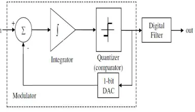
[image:2.595.308.505.375.494.2]The basic block diagram of a discrete-time first order ΣΔ modulator is shown in figure 1. The input signal comes into the modulator via a summing junction. It then passes through the integrator which feeds a comparator that acts as a one-bit quantizer. The comparator output is fed back to the input summing junction via a one-bit digital to analog converter (DAC), and it also passes through the digital filter and emerges at the output of the converter.
Figure 1: Discrete-time first order Sigma-Delta Modulator
The input signal comes into the modulator via a summing junction. It then passes through the integrator which feeds a comparator that acts as a one-bit quantizer. The comparator output is fed back to the input summing junction via a one-bit digital to analog converter (DAC), and it also passes through the digital filter and emerges at the output of the converter.
The SNR of first order noise shaping can be derived as:
) 2 ( ) ( 30 17 . 5 76 . 1 02 .
6 N Log OSR eq
SNR= + − +
Where N is the resolution of the modulator [8]. The advantage of first order noise shaping is an improvement of the SNR by 9 dB for every doubling of the oversampling ratio as opposed to a 3 dB increase without noise shaping. It can be also be proved that implementing a second order ΣΔ
ADC can provide for much better noise shaping and a higher order resolution. Thus, the signal to noise ratio (SNR) is higher for a second order ADC converter [9].
In a discrete-time ΣΔ modulator, the input is a sampled signal. It is possible to realize a continuous-time modulator as shown in figure 2. In this case the input signal and the loop-filter are continuous and the sampling operation only occurs before the quantizer.
Generally, modulators can be implemented either as a sampled-data system or in the continuous-time domain. The primary difference is that sampled-data systems employ switched-capacitor integrators while continuous-time systems use active-RC integrators in the modulators. For this reason Switched-capacitor integrators take advantage of a very small area by eliminating the need for physical resistors. In addition switched-capacitor systems are less sensitive to clock jitter and to the manner in which the operational amplifier settles.
[image:2.595.92.284.377.488.2]
Figure 2: Continuous-Time first order Sigma-Delta Modulator
Finally, the oversampling ratio in switched-capacitor integrators is limited by the achievable bandwidths of the operational amplifier. This makes continuous-time modulators very appealing for high-speed applications.
The expected requirements for our analog-to-digital converter is to operate on low to mid frequency analog signals, at a resolution of 8 bits or higher, and to have power consumption on the order of mill watts in CMOS 0.35um technology.
modulator in which the performance with simulations results of each component is described using CADENCE to confirm the number of bit used in the previous section. In section 3, all main parameters of the described modulator are indicated with a full comparison of the most popular designs, in which the performance of each modulator is cited in table 4, in particular our design to specify the trade-off between higher speed and low power consumption. Conclusion is drawn in Section 5.
2. REVIEW OF SIGMA-DELTA MODULATOR
[image:3.595.301.512.73.259.2]
Figure 3: Block diagram of First Order Sigma-Delta Modulator using MATLAB/Simulink
First order ΣΔ modulators are probably the most common category of the device which has more stability than second order and third order circuit. If we compare first order ΣΔ modulator with the other types in terms of power consumption and size they consumed low power. In addition, the structure of first order ΣΔ modulator has the advantages of being simple, robust and stable.
The functional diagram of the first order modulator simulated using Simulink in MATLAB is shown in figure 3. The single bit DAC is replaced by a simple wire. The input is a sinusoidal signal with 0.9 V amplitude and frequency 40 kHz. This signal is fed through only one integrator and is connected to the comparator at the output.
The modulated output as seen through the scope is shown in figure 4 with the input signal overlaid on it.
Behavioural simulations using MATLAB were carried out to find the optimal number of bits.
0 50 100 150 200 250
-1 -0.8 -0.6 -0.4 -0.2 0 0.2 0.4 0.6 0.8 1
Temps ( X 10.E-7 ) Sec
[image:3.595.91.289.259.398.2]A m p li tu d e ( V )
Figure 4: Delta Sigma Modulation of a Sample Waveform
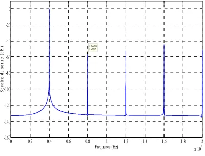
From figure 5, it can be concluded the frequency spectrum of the output that Spurious Free Dynamic Range (SFDR), which is the ratio of the RMS value of the input sine wave for an ADC to the RMS value of the peak spur observed in the frequency domain being 55.15 dB.
0 0.2 0.4 0.6 0.8 1 1.2 1.4 1.6 1.8 2
[image:3.595.307.507.360.512.2]x 105 -160 -140 -120 -100 -80 -60 -40 -20 0 X: 8e+004 Y: -55.15 Frequence (Hz) S p e c tr e d e so rt ie ( d B )
Figure 5: Output power spectrum using MATLAB/Simulink
The resolution of the modulator was calculated from this expression:
) 3 ( 86 . 8 02 . 6 76 . 1 eq bits SFDR
nb = − =
3. DESIGN OF THE FIRST ORDER SIGMA-DELTA MODULATOR
Comparator Clock
Generator
OTA Switchers
[image:4.595.87.508.88.348.2]Source Voltage 1.5V
Figure 6: A complete First order Sigma-Delta modulator using CADENCE
3.1 Design of Basic CMOS OTA
3.1.1 Analyze
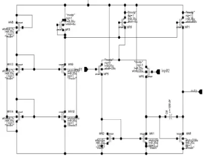
[image:4.595.306.515.455.541.2]The basic CMOS Operational Transconductance Amplifier (OTA) [10] is shown in figure 7. The first stage of OTA contains two input transistors formed by P-channel MOSFETs which are MP5 and MP6, with a current mirror formed by an N-channel MOSFETs: MN1 and MN2. The second stage is a common source amplifier which is formed by only one transistor MN0. The polarisation block is composed of eight transistors: MP0, MP1, MP3, MN9, MN10, MN14, MN13, and MN8.
Figure 7: Basic CMOS Operational Transconductance
Amplifier (OTA)
3.1.2 Simulations results
Table 1 shows simulation results of the OTA with an effective load capacitance of Cl.
Table 1: OTA circuit performance
Parameter OTA
Supply voltage 3 V
DC gain 40 dB
Phase margin 71°
Unity gain frequency 80 KHz Effective load capacitor (Cl) 0.2 pF
Process AMS 0.35 µm
The results are optimized by the size of transistors in table 2 for a supply voltage of 3V. This scheme is simulated using T-spice based BSIM3v3 transistor model for the AMS 0.35µm CMOS technology.
Table 2: Dimensions of transistors of OTA
Transistors W / L
MP5 , MP6 28 / 0.35
MN1 , MN2 6 / 0.35
MP1 60 / 0.35
MN0 220 / 0.35
MN8, MN9, MN10, MN13, MN14 0.7 / 0.35
[image:4.595.90.291.553.709.2]The OTA designed achieves a gain of 40 dB with a large gain bandwidth of 72 MHz and phase margin of 71 degrees for a capacitive load of 0.2 pF. The simulated output frequency response of our OTA is shown in figure 8. These results indicate that the OTA provides satisfactory performance to operate the modulator.
100 1k 10k 100k 1M 10M 100M
Frequency (Hz)
-100 -50 0
M
a
g
n
it
u
d
e
(
d
B
),
P
h
a
s
e
(
d
e
g
[image:5.595.307.504.180.400.2])
Figure 8: Frequency response of Operational Transconductance Amplifier OTA
3.2 Design of Comparator
3.2.1 Analyze
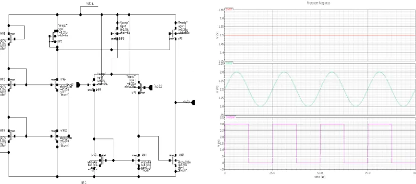
[image:5.595.91.291.220.388.2]A comparator is a device used for ΣΔ modulator. In our case, it compares two voltages and switches its output to indicate which is larger. The basic block of CMOS comparator is shown in figure 9.
Figure 9: Basic CMOS comparator
[image:5.595.97.503.535.715.2]Figure 10 shows the layout of the designed comparator. This circuit is designed by using the 1-poly and 4-metal in AMS 0.35µm technology.
Figure 10: layout of comparator
3.2.2 Simulation results
The comparator is set up by putting the inverting input at 1.5 V and the not inverting at a sinusoidal signal with 0.5 V of amplitude and frequency 40 kHz. When a sine wave is input to the circuit, the comparator switches from positive rail to negative rail as shown in figure 11.
[image:5.595.93.291.537.717.2] [image:5.595.305.505.538.710.2]3.3 Design of Non Ovelapping Clock Phase Generator
[image:6.595.304.507.78.341.2]The non-overlapping clock phase generator was designed as shown in figure 12.
Figure 12: Non-Overlapping Clock Phase Generator Circuit
A series of cascaded inverters with their W/L ratios being less 1 cause a significant delay in the output of the inverter. Figure 13 shows the output of the clock generator
Figure 13: Output of the clock generator
[image:6.595.85.511.80.374.2]Figure 14 shows the layout of the designed phase generator. It is designed by CADENCE using AMS 0.35µm technology process.
Figure 14: Layout of Clock Phase Generator
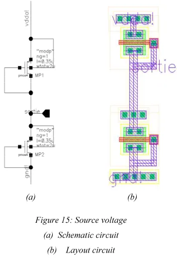
3.4 Design of source voltage
The voltage source is designed to produce a constant value of 1.5V.
As shown in figure 15, it is composed of two transistors formed by P-channel MOSFETs in order to maintain a voltage of 1.5V.
[image:6.595.94.286.191.344.2]
(a) (b)
Figure 15: Source voltage (a) Schematic circuit
[image:6.595.89.291.448.642.2] [image:6.595.325.503.466.730.2]Clock generator
Switches Integrator Comparator
[image:7.595.90.513.85.410.2]Source voltage of 1,5V
Figure 16: A layout of complete first-order Sigma-Delta modulator
3.5 Design of a complete Modulator Sigma-Delta
3.5.1 Analyze
Figure 16 shows a layout of a complete first order ΣΔ modulator. It is made up of only one integrator, a comparator, a source voltage 1.5V and a clock generator. These include switches for applying one of two references node voltages Vrefp and Vrefm,
depending on comparator output polarity. It is indicated that the integrator and the comparator are based on the same amplifier.
3.5.2 Post layout Simulations
To confirm the result of the bit stream in the output of Modulator using MATLAB/Simulink, the figure 17 shows the same result obtained by CADENCE. Here, the pulse density output from a ΣΔ modulator for a sine wave input is presented.
[image:7.595.315.497.458.676.2]
The proposed modulator was designed and simulated in a 0.35µm process. Figure 18 shows the output power spectrum for a 40 KHz sine-wave.
0 0.05 0.1 0.15 0.2 0.25 0.3 0.35 0.4 0.45 0.5
-90 -80 -70 -60 -50 -40 -30 -20 -10 0
Fréquence (X 10E7) Hz
[image:8.595.311.513.148.298.2]S p e ct re d e s o rt ie ( d B ) Figure 18: The post layout simulated output power
spectrum.
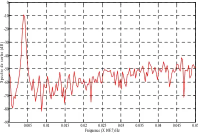
From figure 19, it can be concluded from the frequency spectrum of the output that SFDR is equal to 49.79 dB with the measured SNR is 55 dB. The resolution of the modulator was calculated from this expression:
) 4 ( 98 . 7 02 . 6 76 . 1 eq bits SFDR
nb = − =
The ADC gives number of bit (nb) equal to 8 bits.
This result is the same as given by theoretical using MATLAB/Simulink.
0 0.005 0.01 0.015 0.02 0.025 0.03 0.035 0.04 0.045 0.05 -90 -80 -70 -60 -50 -40 -30 -20 -10 0
Fréquence (X 10E7) Hz
S p e c tr e d e s o rt ie ( d B )
Figure 19: Zoom of figure 17
4. RESULTS AND COMPARISON
[image:8.595.93.289.174.314.2]The modulator is designed using a 0.35um CMOS process, the over sampling ratio is 64 with a signal band width of about 80 kHz. The modulator performance is summarized in table 3.
Table 3: Designed modulator parameters
Parameters Value
Technology AMS 0.35 µm
Order of modulator 1
Sampling Frequency (clock) 10.24 MHz
Signal Band width 80 KHz
Over sample Ratio(OSR) 64
References ±1V
Maximum Input 1 Vpp
Supply voltage 3 V
Resolution 8-bit
Quantizer resolution 1 bit
Power consumption 1.162 mW
Area 8360µm²
(76µm X 110µm)
The current state of the art in the design of ΣΔ modulator is limited by the technology and the sampling speeds it is able to achieve. Here is a comparison table 4 of the most popular designs which also compares the published works with the current work. It can be seen that the current work consumes less power than most published work and achieves the resolution of 8 bits using one of the technology 0.35 μm CMOS process.
5. CONCLUSION
[image:8.595.92.290.508.644.2]Table 4: Comparison Table Of Most Popular Designs With Current Work (*)
Resolution Voltage (V)
Area (mm2)
Speed (MHz)
Power (mW)
Technology (CMOS)
Bandwidth (Khz)
Order Ref
14 bits 3.3 - 2.2 200 0.35µm 100 6 [11]
14 bits 1 - 5 0.95 0.35 µm 25 3 [12]
13 bits 1 0.41 10.24 5.6 0.35µm 50 2 [13]
14 bits - 0.66 0.524 - 0.35µm 2.048 3 [14]
8 bits 3.3 0.57 0.524 - 0.35µm 2.048 1 [15]
12 bits 0.6 2.88 3.072 1 0.35µm 24 2 [16]
14 bits 3.3 - 12.8 2.14 0.35µm 25 2 [17]
15 bits 3 3.11 - 5 0.35µm - 4 [18]
12 bits 3.3 - 1.024 1.4 0.35µm 4 2 [19]
14 bits 3.3 - 1.024 3 0.35µm 4 4 [20]
11 bits 2.5 0.1 0.12 0.5 0.35µm 0.1 3 [21]
8-bit * 3 0.008 10.24 1.162 0.35µm 80 Khz 1 This work
The comparison table of most popular designs is shown in table 4. It compares the published works with the current work. It can be seen that the current work consumes less power of 1.16 mW than most published work and achieves the resolution of 8 bits at higher speed of 10.27 MHz This design gives a good example for the trade-off between speed and power consumption.
Future work to extend the current design could be design optimization. For example, Miller operational transconductance amplifier designed can be gain boosted for enhanced noise shaping. Use of multi-bit ADC and DAC also can help increasing the resolution of the modulator. Dithering can also help increase the SNR. Dithering is a technique of intentional addition of white noise in the circuit which has proven to yield better in-band noise attenuation. The first order modulator can be cascaded to a second order modulator to decrease the noise shaping. Also in order to design a complete ADC, it is necessary to add a decimation filter with modulator. A using of this decimation filter is one of the important blocks. Because it low-pass filters the output signal from the quantizer. Hence all of the quantization noise that doesn’t appear within the bandwidth. Then filtering action that precedes the down-sampling operation ensures that aliasing doesn’t occur. Finally the purpose of this paper is to design and fabricate the chip using AMS 0.35µm CMOS technology.
REFRENCES:
[1] Vineeta Upadhyay and Aditi Patwa, “Design Of First Order And Second Order Sigma Delta Analog To Digital Converter”, International Journal of Advances in Engineering & Technology, July 2012.
[2] J. Bourgette, D. Cavalari, B. Luo, “Design and Testing of a 0.25 um 12-bit Analog-to-Digital Converter,” WIT, October 2001.
[3] C. Aust, “A Low-Power, Variable-Resolution Analog-to-Digital Converter,” Virginia Tech, June 2000
[4] S.R. Norsworthy, R. Schreier, G.C. Temes, “Delta-Sigma Data Converters,” (New York, IEEE Presss, 1997)
[5] V. Peluso, M. Steyaert, W. Sansen, “Design of Low-Voltage Low-Power CMOS Delta-Sigma A/D Converters,” (Kluwer Academic Publishers, Boston, MA, 1999).
[6] Mohammed Arifuddin Sohel, K. Chenna Kesava Reddy, Syed Abdul Sattar, “Design of Low Power Sigma Delta ADC”, International Journal of VLSI design & Communication Systems (VLSICS) Vol.3, No.4, August 2012
[7] YiWu et al, « Multi-Bit Sigma Delta ADC with Reduced Feedback level, Extended Dynamic Range and Increased Tolerance for Analog Imperfections » IEEE 2007 Custom Integrated Circuits Conference (CICC).
[9] K L Lee, R G Meyer. Low-Distortion Switched-Capacitor Filter Design Techniques [J].I EEE J.Solid-State Circuits, 1985, 20(6):1103-1113. [10] Radwene Laajimi & Mohamed Masmoudi:”A
Novel Design of Two-Stage CMOS Amplifier Used For Sigma-Delta Analog to Digital Converter”, 2012 International Conference on Design & Technology of Integrated Systems in Nanoscale Era
[11] Morizio, J.C.; Hoke, M.; Kocak, T.; Geddie, C.; Hughes, C.; Perry, J.; Madhavapeddi, S.; Hood, M.H.; Lynch, G.; Kondoh, H.; Kumamoto, T.; Okuda, T.; Noda, H.; Ishiwaki, M.; Miki, T.; Nakaya, M. "14-bit 2.2-MS/s sigma-delta ADC's", Solid-State Circuits, IEEE Journal of, On page(s): 968 - 976 Volume: 35, Issue: 7, July 2000
[12] M. Dessouky, and A. Kaiser. Very Low-Voltage Digital-Audio 6. L Modulator with 88-dB Dynamic Range Using Local Switch Bootstrapping. IEEE J. Solid-State Circuits,2001, 36 (3) :349-355.
[13] M. Keskin, U. Moon, and G. C. Ternes. A I-V 10-MHz Clock-Rate 13-Bit CMOS L 6. Modulator Using Unity-Gain-Reset Opamps. IEEE J. Solid-State Circuits, 2002, 37 (7): 822 [14] D. Milovanovic, M. Savic and M. Nikolic ,"A
Third Order Sigma-Delta Modulator", Microelectronics, 2004. 24th International Conference on, 16-19 May 2004
[15] Dragiša Milovanovi, Milan Savi and Miljan Nikoli," SECOND-ORDER SIGMA-DELTA
MODULATOR IN STANDARD CMOS
TECHNOLOGY", Proc. XLVIII ETRAN Conference, aak, June 6-10, 2004, Vol. I [16] G. Ahn, D. Chang, M. E. Brown, et al. A 0.6-V
82dB Deta-Sigma Audio ADC Using Switched-RC Integrators. IEEE J. Solid-State Circuits, 2005, 40 (12) : 2398-2405
[17] S.K. Nathany," Design of fully differential discrete time Delta-Sigma modulator", These, Rochester institute of technology, New York, 2006.
[18] Hsin-Liang Chen ; Tamkang Univ., Taipei ; Yi-Sheng Lee ; Jen-Shiun Chiang,"Low power sigma delta modulator with dynamic biasing for audio applications",Circuits and Systems, 2007. MWSCAS 2007. 50th Midwest Symposium on 5-8 Aug. 2007
[19] Fun Ye, Jen-Shiun Chiang, and Chun-Cheng Wu ,"Low Power Sigma-Delta Modulator with Dynamic Biasing for Speech CODECs", Proceedings of the International Conference on Embedded Systems and Applications, ESA '04
& Proceedings of the International Conference on VLSI, VLSI '04, June 21-24, 2004, Las Vegas, Nevada, USA
[20] Sangyong Lee,Wonki Park, Kyongwon Min , Byong-Deok Choi ,SungChul Lee, "Sigma-Delta (Σ-Δ) ADC for Complex Sensor Applications", International Technical Conference on Ci, Vol.2009 No.7, 2009 [21] Chen Jin et al 2010," Low-power
switched-capacitor delta-sigma modulator for EEG recording applications ", J. Semicond. 31 075009. doi:10.1088/1674- 4926/31/7/075009 Received 18 September 2009, in final form 7 February 2010.