© 2016, IRJET | Impact Factor value: 4.45 | ISO 9001:2008 Certified Journal
| Page 830
Design and Implementation of 128-bit SQRT-CSLA using
Area-delay-power efficient CSLA
Nagaraju Tatipudi
1and TVS Divakar
21
M. Tech Scholar, Department of ECE, GMR Institute of Technology, Rajam, Srikakulam, Andhra Pradesh, India.
2
Sr. Assistant Professor, Department of ECE, GMR Institute of Technology, Rajam, Srikakulam,
Andhra Pradesh, India.
---***---
Abstract—
In VLSI, area, delay and power are the crucialparameters. To minimize them we have a lot of methods, but there is still a requirement of a robust algorithm to reduce them. By the use of efficient carry select adder, we can optimize the area, delay, power compared to the conventional adders. The conventional carry select adder (CSLA) and BEC-based CSLA adder are the references, on analysing these adders we have observed the data dependency and identified theunnecessary logic operations, on remove all the unnecessary logic operations existent in conventional CSLA, the proposed new logic formulation for conventional CSLA works effectively with less area and less delay than newly proposed BEC-based method, in consequence of small carry output delay. The proposed method is suitable for SQRT- CSLA, which gives better results than conventional SQRT-CSLA which has less area, less delay for different bit widths, on an average. Results of synthesis show that BEC- SQRT CSLA design consumes more energy and more ADP than proposed SQRT-CSLA on average, for different bit widths. Furthermore, in this paper, we have proposed 128-bit SQRT-CSLA with proposed CSLA.
Index Terms—VLSI, CSLA, Area-delay-power efficient design, SQRT-CSLA, Xilinx.
I. INTRODUCTION
Adder is a digital circuit that works on binary bits for addition operation. Generally, the adder is used in the arithmetic logic unit, which plays a key role. It is also used in some other parts of the processor for calculating the address, table indices, increment and decrement operators, and similar operations. These are the references, for increasing significant priority of adders in electronics. Several adders are used in complex digital signal processing (DSP) system. An efficient adder can give
the high performance, area efficient, low power, for the complex DSP systems. High performance, low power, area efficient VLSI designs are utilized as a part in mobile devices, Multistandard remote beneficiaries and biomedical instrumentation [1] [2]progressively used, for these three parameters mainly depends on efficient adder. Ripple carry adder (RCA) is a simple design adder, in RCA carry propagation is the main concern. To minimize the carry propagation delay (CPD), carry look-ahead adder and carry select adders are have been recommended. The conventional CSLA has RCA-1 unit, RCA-2 unit and selection unit, the RCA-1 and RCA-2 units are generates pair of sum words and output carry bits accordingly to their relative anticipated input carry (Cin = 0 & 1), then selection unit select the one out of the sum word and one out of the output carry bits, these are the final sum and final output carry [3] respectively. The CSLA gives better performance in terms of CPD but the design is bit complicated, due to the dual use of RCAs. Few attempts have been made to ignore the use of RCA as twice. Instead of has two RCAs. Kim and Kim [4] have implemented with one RCA circuit and one add-one circuit which is operated with mux.
© 2016, IRJET | Impact Factor value: 4.45 | ISO 9001:2008 Certified Journal
| Page 831
The main purpose of proposing SQRT-CSLA is to provide aparallel path for carry propagation, which involves directly to minimize the overall adder delay. However, the more logic resources and high delay are required in CBL-based SQRT-CSLA design [8] than BEC-based SQRT CSLS design of [6].
The logic optimization and adder delay are analysed for the existing methods and observed. In this analysis, logic optimization is highly depending on redundant logic operations present in the logic formulation and the adder delay is data dependent. It is also observed that a high priority is given for logic optimization while less literature on data dependence. The logic formulations of CSLA and BEC-based CSLA are examine to study the data dependency and identify the unnecessary logic operations involved in it. This is a reference to proposed new logic formulation for CSLA, this logic formulation based on the data dependence and optimized logic operations are to optimize carry generate (CG), optimize carry select (CS) design. In this paper, the proposed CSLA extended to higher bit-width to increase performance.
Using proposed CSLA logic formulation, derive an efficient logic design for CSLA, for this logic optimization the proposed CSLA has significantly less ADP than conventional CSLA adders. The proposed CSLA utilized in SQRT-CSLA closely shows that 32% less ADP and absorb 33% less energy than existing SQRT-CSLA. In this paper the proposed CSLA based SQRT-CSLA is extended to higher bit widths. Rest of this paper as follows. Logic formulation of CSLA is having in section II. The proposed CSLA is represented in Section III and the performance comparison is represented in Section IV. The results is mention in Section V, The conclusion is mention in Section VI.
II. LOGIC FORMULATION
The basic CSLA combination of two n-bit RCAs called as sum and carry generating unit (SCG), and sum and carry selection unit (SCS) [9]. SCG unit takes most of the logic resources and it contributes major role in critical path. Different methods are proposed for optimized SCG unit. It is studied that the logic design of the SCG unit [6]. The main motto for this study is to identify the redundant logics operations and data dependence, then eliminating all the redundant operations and sequential operations
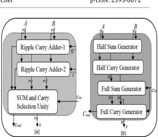
Fig. 1 Logic Block Diagram of: (a) Conventional Carry Selector Unit, and (b) Ripple Carry Adder
RCA block has these four sub-blocks: half sum generator (HSG) unit, half carry generator (HCG) unit, full sum generator (FSG) unit and full carry generator (FCG) unit. The HSG block generates sum and carry output using the conventional half adder circuit using the corresponding bits of the CSLA. It consists of N numbers of XOR gates and AND-gates to perform the operation.
A.
Conventional CSLA Logic Expressions for SCG
Unit.
The above figure. 1 shows the conventional CSLA, SCG unit consist of two RCAs with N-bit words. By adding these N-bit words in conventional CSLA, the sum and carry generating unit generates n-bit sum words (S0
and S1) and output carry bits (C and C ) with their
respective input carry ‘0’ and ‘1’. Basically, the operation performed in RCA is in four steps shown in figure 1(b), those are half-sum generation (HSG), half-carry generation (HCG), full-sum generation (FSG), full-carry generation (FCG).
The logic formulations of sum and carry generating (SCG) unit of n-bit CSLA are following.
) ( ) ( ) ( 0 0
i B i A i
s ( ) () ( )
0 0
i B i A i
[image:2.612.323.575.71.290.2]© 2016, IRJET | Impact Factor value: 4.45 | ISO 9001:2008 Certified Journal
| Page 832
) 1 ( 1 0 ) ( 0 ) ( 0 0 ) (1 i c i
o s i c i o
c (1b)
) 1 ( 1 0 ) ( 0 ) ( 0 0 ) (
1 i c i
o s i c i o
c ( 1)
1 0 0
c n out c (1c) ) ( ) ( ) ( 0 1 i B i A i
s () () () 0 1 i B i A i
c (2a)
) 1 ( 1 1 ) ( 0 1 ) ( 1 1
s i c i
i s (2b) ) 1 ( 1 1 ) ( 0 1 ) ( 0 1 ) ( 1 1
c i s i c i
i
c ( 1)
1 1 1
c n
out c
(2c)
Where ( 1), 0 1.
1 1 , 0 ) 1 ( 1 0
c and i n n
c
As shown in the equation are identical that of so that remove these redundant logics to optimize the RCA 2. The HSG and HCG of RCA 1 are shared to build RCA 2. By doing this, the RCA 2 is replaced by one add-one circuit. Later it is known as BEC circuit [6]. Since BEC-based CSLA gives better performance in terms of area-delay-power than existing CSLAs. Now we discuss the logic formulation of BEC-based CSLA of SCG unit.
B.
The Logic expressions of the sum and carry
generating Unit according with BEC-based
CSLA
.As shown in fig.2, the RCA block determine the N-bit sum with respective input carry ‘0’. These values are fed to the BEC unit, which receives and generates ( -bit excess-1 code. The MSB of BEC unit represents as and LSB of the BEC unit represents .
[image:3.612.329.521.378.532.2]The structure of the BEC-based CSLA is the better one than the conventional CSLA in terms of complexity, which means logic formulation and sequential operations. Which can be proved by the following figure and following equations.
Fig. 2. Block diagram of the BEC-based CSLA; n is the input operand bit-width
So the logic equations of RCA are 1(a)-1(c), and the BEC unit equations are follows
) 0 ( 1 0 ) 0 ( 1 1 s
s (0)
1 0 ) 0 ( 1 1 s
c (3a)
(3b) ) 1 ( 1 1 ) ( 1 0 ) ( 1 1
s i c i
i
c (3c)
) 1 ( 1 1 ) 1 ( 1 0 1
c n c n
out c
(3d)
1
1
i
n
for
The logic formulations 1(a) to 1(c) and 3(a) to 3(d) are represent the BEC-based CSLA of SCG unit. In this high data dependence is seen. By observing the equation 3(a), depending on , which does not happen in conventional CSLA. With this, the further study on logic formulations of conventional CSLA for data dependence to get efficient logic formulation for conventional CSLA is done. With this study, all the redundant logic formulations are removed from the equations 1(a) to 1(c) and 2(a) to 2(c) and rearrange these as proper manner by using their data dependence. Those rearranged logic formulations are followed as ) 1 ( 1 1 ) ( 1 0 ) ( 1 1
s i c i
© 2016, IRJET | Impact Factor value: 4.45 | ISO 9001:2008 Certified Journal
| Page 833
)( ) ( ) (
0 i Ai Bi
s () () ( )
0 i Ai B i
c
(4a)
) ( 0 ) ( 0 ) 1 ( 1 0 ) ( 1 0
i c i s i c i
c (0) 0)
1 0
(c
for
(4b)
) ( 0 ) ( 0 ) 1 ( 1 1 ) ( 1 1
i c i s i c i
c (0) 1)
1 1 (c for
(4c) )
( 1 0 )
(i c i
c ( 0)
in c if
(4d) )
( 1 1 )
(i c i
c ( 1)
in c if
(4e) )
1
(
c n
out c
(4f)
in c s
s (0)
0 ) 0
( () ( 1)
0 )
(i s i c i s
(
4
g
)
III. PROPOSED ADDER DESIGN
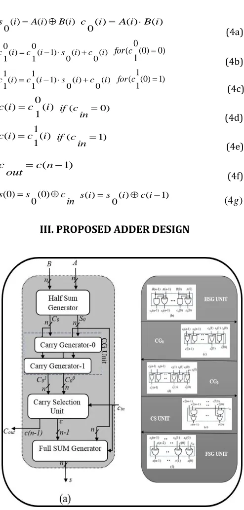
Fig. 3. (a) Proposed CS adder design, where n is the input operand bit-width, (b) Gate-level composition of the half sum generator. (c) Gate-level optimized composition of carry generator with input carry = 0. (d) Gate-level optimized composition of carry generator with input carry = 1. (e) Gate-level composition of the carry selection unit. (f) Gate-level composition of the final-sum generation unit.
The above figure 3(a) shows the designing of the adder, by using the logic formulations of the 4(a) to 4(g). In which totally four units are there, those are HSG, CG, CS and FSG. The HSG generates n-bit half-sum word S0 and half-carry
word C0, by considering inputs as two n-bit words that are
A and B. These S0 and C0 fed to the CG unit. The CG unit is
composed of two units of CG0 and CG1and these both are
receives the S0 and C0, than generates n-bit full-carry word
for their respective input carry bits (Cin=0 and
Cin=1) and the CG unit is optimized by the advantages of
fixed carry-inputs, the respective optimized circuit shown above as figure 3(c) and 3(d). The n-bit full-carry word
are fed to CS unit, the CS unit select the one carry bit from , that’s as an final-carry bit, by
the use of control bit Cin
. The CS unit is implemented by 2-to-1 Multiplexer, however the carry words of CS unit is specific pattern that is irrespective of half-sum word S0 and half-carry word C0, for
This pattern is used in logic optimization of CS unit, which shows in figure 3(e).The is the final carry word from CS unit. This proposed adder gives much better results in SQRT-CSLA. Here we have worked on 128-bit SQRT-CSLA with proposed CSLA.
IV. PERFORMANCE COMPARISON
[image:4.612.40.287.90.607.2]© 2016, IRJET | Impact Factor value: 4.45 | ISO 9001:2008 Certified Journal
| Page 834
delay in CSLA stages of SQRT-CSLA is crucial for theoverall adder delay. By the multipath carry propagation feature in proposed CSLA, the output-carry is generated earlier by this early generation of
Output carry, which is very suitable for SQRT-CSLA than existing CSLA designs for area-delay efficient implementations of SQRT-CSLA.
Fig. 4. Proposed SQRT-CSLA for n = 16. All intermediate and output signals are define with delay (displayed in square brackets).
TABLE 1
SIMULATION AND SYNTHESIS RESULTS OF SQRT-CSLA FOR DIFFERENT BIT-WIDTHS
The figure 4 shows the 16 bit SQRT-CSLA design of proposed CSLA, where we are used 2-bit RCA, 2-bit CSLA, 3-bit CSLA, 4-bit CSLA and 5-bit CSLA. To show the advantages of SQRT-CSLA with the using of proposed CSLA than conventional SQRT-CSLAs [6], [7]. The different bit-widths 16, 32, 64 and 128 were displayed in the Table V.
the CBL-based SQRT-CSLA [7] has the significantly higher delay for large bit-widths than proposed SQRT-CSLA and BEC-based SQRT-CSLA. The proposed SQRT-CSLA has less ADP than BEC-based SQRT-CSLA [6], and CBL-based SQRT-CSLA [7] on average, for different bit-widths.
V. RESULTS
We have coded the conventional CSLA for 8-bit and 16-bit, proposed CSLA for 8-bit and 16-bit, SQRT-CSLA with the conventional CSLA design for 8-bit, 16-bit, 32-bit, 64-bit and 128-bit, SQRT-CSLA with the suggested CSLA design for 8-bit, 16-bit, 32-bit, 64-bit and 128-bit in VHDL. All the designs are synthesized in the Xilinx ISE Design Suite 14.2. The proposed SQRT-CSLA involves significantly less area and less delay and consumes less power than the existing designs.
PROPOSED SQRT-CLSA 128-bit, RTL SCHEMATIC
[image:5.612.37.287.212.375.2]© 2016, IRJET | Impact Factor value: 4.45 | ISO 9001:2008 Certified Journal
| Page 835
PROPOSED SQRT-CSLA 128, RADIX IN HEXADECIMALVI. CONCLUSION
The logic operations of conventional CSLA and BEC-based CSLA were analyzed to study the unnecessary logic operations and determine the dada dependence. Than eliminate all the sequential operations and unnecessary logic operations then proposed a new logic formulation for the conventional CSLA. In the proposed CSLA the process of carry selection is schedule before calculation of final-sum, which gives the optimize results of proposed CSLA and it is new approach compare to conventional approach. For the carry word the corresponding carry inputs are ‘0’ and ‘1’ based on the proposed CSLA follow a specific bit pattern, which optimize the CS unit. And where fixed input bits of CG unit is also optimize the logic formulation of CG unit, based on this optimized logic of CS and CG units, an efficient logic formulation is obtained for CSLA. And this logic formulation involves significantly less area and delay than the latest method of BEC-based CSLA, due to less output-carry delay. And this proposed CSLA very much suitable and better to use in SQRT method than conventional SQRT methods. And using proposed CSLA in SQRT method (SQRT-CSLA), results are more ADP and it consumes more energy in BEC-based SQRT CSLA compare to proposed SQRT-CSLA, on average for variant bit widths.
REFERENCES
[1] K. Mohanty and S. K. Patel, "Area–Delay–Power Efficient Carry-Select Adder," in IEEE Transactions on Circuits and Systems II: Express Briefs, vol. 61, no. 6,
pp. 418-422,
June2014.doi:10.1109/TCSII.2014.2319695.
[2] K. K. Parhi, VLSI Digital Signal Processing. New York, NY, USA: Wiley, 1998.
[3] A. P. Chandrakasan, N. Verma, and D. C. Daly, “Ultralow-power electronics for biomedical applications,” Annu. Rev. Biomed. Eng., vol. 10, pp. 247–274, Aug. 2008.
[4] O. J. Bedrij, “Carry-select adder,” IRE Trans. Electron. Comput., vol. EC-11, no. 3, pp. 340–344, Jun. 1962. [5] Y. Kim and L.-S. Kim, “64-bit carry-select adder with
reduced area,” Electron. Lett., vol. 37, no. 10, pp. 614– 615, May 2001.
[6] Y. He, C. H. Chang, and J. Gu, “An area-efficient 64-bit square root carry select adder for low power application,” in Proc. IEEE Int. Symp. CircuitsSyst., 2005, vol. 4, pp. 4082–4085.
[7] B. Ramkumar and H.M. Kittur, “Low-power and area-efficient carry-selectadder,” IEEE Trans. Very Large Scale Integr. (VLSI) Syst., vol. 20, no. 2, pp. 371–375, Feb. 2012.
[8] I.-C. Wey, C.-C. Ho, Y.-S. Lin, and C. C. Peng, “An area-efficient carry select adder design by sharing the common Boolean logic term,” in Proc.IMECS, 2012, pp. 1–4.
[9] S.Manju and V. Sornagopal, “An efficient SQRT architecture of carry select adder design by common Boolean logic,” in Proc. VLSI ICEVENT, 2013, pp. 1–5. [10] B. Parhami, Computer Arithmetic: Algorithms and
Hardware Designs, 2nd ed. New York, NY, USA: Oxford Univ. Press, 2010.