e-ISSN: 2278-067X, p-ISSN: 2278-800X, www.ijerd.com
Volume 10, Issue 4 (April 2014), PP.86-93
FPGA Implementation of QPSK modulator by using
Hardware Co-simulation
Preksha R. Kolankar
1, Swati V. Sakhare
21 M.E.Student, Department of Electronics & Telecommunications Amravati University, Amravati, MS, India 2Asst. Prof, Departments of Electronics & Telecommunications Amravati University, Amravati, MS, India
Abstract:- The modulators are the basic requirement of communication systems they are designed to reduce the
channel distortion & to use in RF communication hence many type of carrier modulation techniques has been already proposed according to channel properties & data rate of the system. QPSK (Quadrature Phase Shift Keying) is one of the modulation schemes used in wireless communication system due to its ability to transmit twice the data rate for a given bandwidth. The QPSK is the most often used scheme since it does not suffer from BER (Bit Error rate) degradation while the bandwidth efficiency is increased. It is very popular in Satellite communication. As the design of complex mathematical models such as QPSK modulator in „pure HDL‟ is very difficult and costly; it requires from designer many additional skills and is time-consuming.
To overcome these types of difficulties, the proposed QPSK modulator can be implemented on FPGA by using the concept of hardware co-simulation at Low power. In this process, QPSK modulator is simulated with Xilinx System Generator Simulink software and later on it is converted in Very high speed integrated circuit Hardware Descriptive Language to implement it on FPGA. Along with the co-simulation, power of the proposed QPSK modulator can be minimized than conventional QPSK modulator. As a conclusion, the proposed architecture will not only able to operate on co-simulation platform but at the same time it will significantly consume less operational power.
Keywords:- QPSK, VHDL, FPGA, Xilinx
I.
INTRODUCTION
Modulation is the method of transmitting data signal over carrier signal to minimize the distortion in channel. In Digital modulation, the digital information is transferred as a series of ones (1) and zeros(0) as input signal and amplitude, frequency or phase of carrier signal is shifted according to digital input, so this technique is also known as shift keying. But in digital modulation, instead of varying the amplitude or the frequency of the carrier signal, it is preferred to vary the phase because it offers better protection in transmitting signals.
Different PSKs can be obtained by M-ary PSK, where M is the no. of states or no. of phase shifts which is depend upon the no. of signals are combined for modulation. In QPSK two signals are combined for modulation. BER of QPSK is better than higher order PSK signals such as 8-PSK, 16-QAM, 32-QAM etc. which are easily affected by noise. At higher order PSK, larger bandwidth is require for higher data transfer rate and consume more power, whereas QPSK is more bandwidth as well as power efficient. There are many applications where QPSK modulator is used, out of which few are of battery operated devices such as Bluetooth, TDMA cellular communication, Medical Implant Communication Services (MICS) etc. therefore it is necessary to minimize the power consumption of these devices so that the battery will last for longer time. It can be done by reducing the speed of operation.
II.
QPSK
MODULATOR
III.
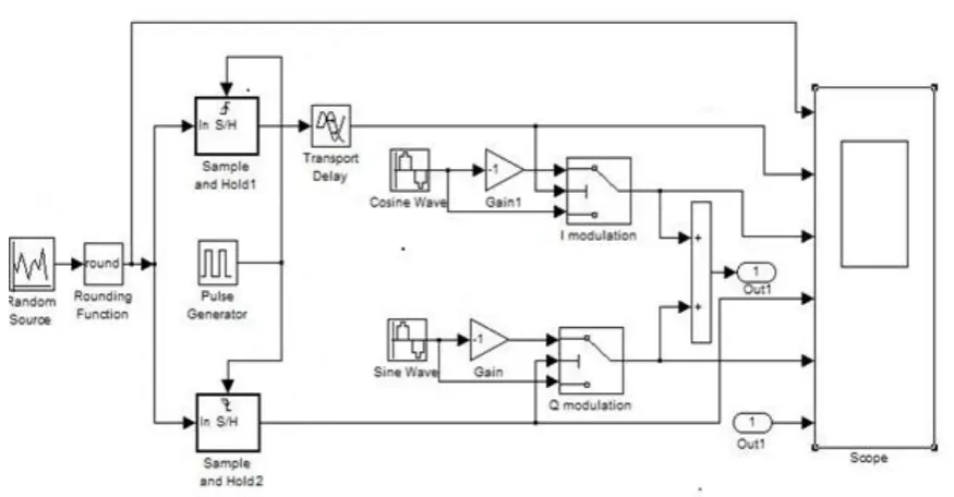
QPSKMODULATOR IN SIMULINKThe Simulink block set contains: The random source and rounding function blocks which generate the binary sequence or the modulating signal.
The binary sequence is separated into an odd-bit sequence I and an even-bit-sequence Q with the help of the sample-and-hold block. The Sample and Hold block acquires the input when it receives a trigger event at the trigger port (rising, falling or either edge). The block then holds the output at the acquired input value until the next triggering event occurs. The odd bits are acquired at the rising edge triggers: when the trigger input rises from a negative value or zero to a positive value and the even-bits are acquired at the falling edge triggers: when the trigger input falls from a positive value or zero to a negative value. Because the I sequence is read first, it has been delayed with the Transport Delay block in order to be synchronized with the Q sequence.
The cosine wave block generating a cosine waveform and with the help of the gain block, a cosine with 180º phase difference for the I-channel, and for the Q-channel: the sine wave block which generates a sinus waveform and with the help of the gain block, a sinus with phase difference of 180º.
The switch blocks which will choose between the first or third output depending on the value of the second input. In the case of the I-channel, if the second input is “1”, the output value will be cosine, but if the second input is “0”, the output will be –cosine and for the Q-channel, if the second input is “1”, the output value
11
01
00
Figure2:QPSK Modulator in the Simulink environment.
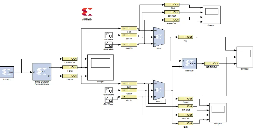
Figure 4. QPSK Modulator in System Generator.
System Generator is a digital signal processing design tool from Xilinx. It is based on the Matlab/ Simulink environment used for FPGA design. Designs are made in the Simulink environment using a Xilinx specific blockset. All implementation steps, including synthesis, place and route are automatically performed to generate an FPGA programming file. Fig.4 illustrates the implementation of a QPSK Modulator using System Generator tools in Simulink.
The System Generator Blockset contains: gateway in blocks:It is used for giving inputs to the Xilinx portion of the Simulink design; gateway out blocks: It is output from the Xilinx portion of the Simulink design;
LFSR block: It implements a Linear Feedback Shift Register which is used to create the binary sequence or modulating signal.
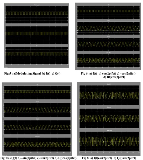
Time Division Demultiplexer block: It accepts input serially and presents it to multiple outputs to a slower rate. In another word, this block divides the modulating signal into the odd-sequence I and even-sequence Q. The division take places inside the FPGA Fig.5 illustrate the waveforms from the first scope in System Generator. In order to see any signal on the scope, the signal must be passed through a gateway out.
Fig 5 : a)Modulating Signal b) I(t) c) Q(t) Fig 6: a) I(t) b) cos(2pifct) c) –cos(2pifct) d) I(t)cos(2pifct)
Fig 7:a) Q(t) b) –sin(2pifct) c) sin(2pifct) d) I(t)cos(2pifct) Fig 8: a) I(t)cos(2pifct) b) Q(t)sin(2pifct)
Figure 9: Block Diagram of System Generator
When System Generator compiles, it automatically wires the imported module and associated files into the surrounding netlist. Xilinx system generator is a very useful tool for developing computer vision algorithms. It could be described as a timely, advantageous option for developing in a much more comfortable way than that permitted by VHDL or Verilog hardware description languages (HDLs).
Matlab-Simulink is an environment for multidomain simulation and Model-Based Design for dynamic and embedded systems. Matlab-Simulink is used in this application as the high level development tool in the design process. Xilinx System Generator is a system-level modeling tool from Xilinx that facilitates FPGA hardware design. It extends Simulink in many ways to provide a modeling environment well suited for hardware design. The result can be synthesized to Xilinx FPGA technology using ISE tools. All of the downstream FPGA implementation steps including synthesis and place and route are automatically performed to generate an FPGA programming file. It also provides a system integration platform for the design of DSP FPGAs that allows the RTL, Simulink, MATLAB and C/C++ components of a DSP system to come together in a single simulation and implementation environment. System Generator supports a box block that allows RTL to be imported into Simulink and co-simulated with either ModelSim or Xilinx ISE Simulator.
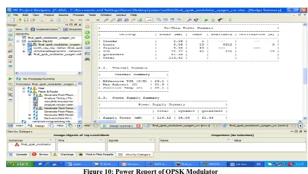
Power Analysis:
Figure 10: Power Report of QPSK Modulator
Hardware-Software Co-simulation
System Generator the use of simulates automatically launching an HDL simulator, generating additional HDL as needed (analogous to an HDL testbench), compiling HDL, scheduling simulation events, and handling the exchange of data between the Simulink and the HDL simulator. This is called HDL co-simulation.
System Generator provides hardware co-simulation, making it possible to incorporate a design running in an FPGA directly into a Simulink simulation. "Hardware Co-Simulation" compilation targets automatically create a bit-stream and associate it to a block as shown in given figure.
Figure 11: FPGA based Hardware-Software (HW-SW)co-simulation Environment
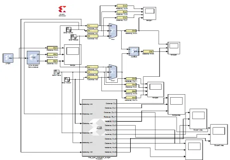
Figure 12: QPSK Modulator in System Generator by using JTAG communication
IV.
C
ONCLUSIONSIn this paper we have proposed a design of QPSK modulator on FPGA which consumes low power and by using Hardware co-simulation, the reduction in hardware requirement cost is achieved. Because after implementing bit stream file on FPGA kit, the result(waveforms)can be observed on matlab simulink itself, instead of using digital oscilloscope, which provide direct communication between FPGA board and PC. Because of these advantages, area and power consumption can be reduced.
REFERENCES
[1] Asaraf Mohamed Moubark,”FPGA implementation of low power digital QPSK modulator using verilog HDL”,Journal of Applied Sciences 13(3),2013,385-392,ISSN 1812-5654
[2] Gaurav Purohit, Divya Vyas, Kota Solomon Raju, V.K Chaubey,Arvind Nehra “Hardware
Co-simulation of BPSK and QPSK For SoftwareDefineRadio”;IJECET,2013,pp 301-308.
[3] Swapan K Samaddar, Atri Sanyal, Somali Sanyal,“ FPGA based generalized architecture for
Modulation and Demodulation Techniques”Journal of Computing Technologies ISSN 2278–
3814,2012,27-32
[4] S.O. Popescu, A.S.Gontean and D.Ianchis; “QPSK Modulator on FPGA”, IEEE 9th International