THESIS
AN OUTLIER DETECTION APPROACH FOR PCB TESTING BASED ON PRINCIPAL COMPONENT ANALYSIS
Submitted by Xin He
Department of Electrical and Computer Engineering
In partial fulfillment of the requirements For the Degree of Master of Science
Colorado State University Fort Collins, Colorado
Spring 2011
Master’s Committee:
Advisor: Anura P. Jayasumana Yashwant K. Malaiya
Copyright by Xin He 2011 All Rights Reserved
ii ABSTRACT
AN OUTLIER DETECTION APPROACH FOR PCB TESTING BASED ON PRINCIPAL COMPONENT ANALYSIS
Capacitive Lead Frame Testing, a widely used approach for printed circuit board testing, is very effective for open solder detection. The approach, however, is affected by mechanical variations during testing and by tolerances of electrical parameters of components, making it difficult to use threshold based techniques for defect detection. A novel approach is presented in this thesis for identifying boardruns that are likely to be outliers. Based on Principal Components Analysis (PCA), this approach treats the set of capacitance measurements of individual connectors or sockets in a holistic manner to overcome the measurement and component parameter variations inherent in test data.
Effectiveness of the method is evaluated using measurements on different types of boards. Based on multiple analyses of different measurement datasets, the most suitable statistics for outlier detection and relative parameter values are also identified.
Enhancements to the PCA-based technique using the concept of test-pin windows are presented to increase the resolution of the analysis. When applied to one test window at a time, PCA is able to detect the physical position of potential defects. Combining the basic and enhanced techniques, the effectiveness of outlier detection is improved.
The PCA based approach is extended to detect and compensate for systematic variation of measurement data caused by tilt or shift of the sense plate. This scheme
iii
promises to enhance the accuracy of outlier detection when measurements are from different fixtures. Compensation approaches are introduced to correct the ‘abnormal’ measurements due to sense-plate variations to a ‘normal’ and consistent baseline. The effectiveness of this approach in the presence of the two common forms of mechanical variations is illustrated. Potential to use PCA based analysis to estimate the relative amount of tilt and shift in sense plate is demonstrated.
iv
ACKNOWLEDGEMENTS
After finishing the thesis, it is time to thank all the people who have helped me so much in the past, which makes this thesis possible and enjoyable for me.
First of all, I would like to give my deepest appreciation to my research advisor, Professor Jayasumana, for providing me such a great opportunity to work with him. I couldn’t thank him enough for his knowledgeable guidance, valuable suggestions, and continuous encouragement throughout my Master study. His tremendous help is always around whenever I need. His vision and knowledge have not only stimulated my passion on research but also taught me many ways in my personal life. I am deeply grateful to the efforts, patience, and enthusiasm that he shared with me along this entire process.
I would also like to thank Professor Malaiya who devoted lots of time into my research. His help is complementary to what Dr. Jayasumana did. From the communication with him, I benefited from both his intelligence and his humor, which will be important to my future life.
Thanks Professor Reising for being on my thesis committee and for their valuable time spent on reading and commenting on my thesis. His passion on research and language produced extremely positive influence on my study and work.
I would like to acknowledge Dr. Kenneth Parker for providing me the opportunity to access Agilent dataset and test background. Thanks to Mr. Steve Hird, Mr. Kent Carey of Agilent, and the Agilent University Relations program for their generous support.
v
I have also benefited greatly from the interaction and collaboration with all the members of the CNRL group at Colorado State University. Their intelligence, dedication, and fantastic personalities make it a learning experience for me everyday. Thanks for their helpful discussion and encouragement when I felt frustrated.
Last but not least, I am so grateful to my parents who helped me develop the interest in science during my childhood. Thank for their love, encouragement, and support during my whole life, especially when I am thousands of miles away from them in the last few years. Finally, I would like to thank my wife, who bought me endless happiness and took care of my life in every single aspect whole heartedly.
vi
TABLE OF CONTENTS
Chapter 1. Introduction………1
Chapter 2. Capacitive Frame Lead Testing………6
2.1. Background………..6
2.2. Principals………..7
2.3. Advantage and challenges………9
2.4. Improved approach………10
Chapter 3. Principal Components Analysis Based Outlier Detection………18
3.1. Introduction to PCA………..19
3.2. Mathematical representation of PCA………20
3.3. Outlier detection with PCA………...24
3.4. Test statistics……….………24
Chapter 4. PCB Test Data Sources………28
4.1.Background for board test………28
4.2.PCB Measurements Datasets………...33
Chapter 5. PCA Analysis of Board Measurements with d Statistics……….37
5.1.Analysis of Measurements of a Single Connector with Principal Components….37 5.1.1. PCA Result for Data3_j24……….39
5.2. Selections of Test Statistics and PC………42
5.2.1. ‘d’ Statistics with Most Significant PCs………...42
5.2.2. ‘d’ Statistics with Least Significant PCs………...47
vii
5.3. Further Test with Multiple Connector Measurements………...54
5.3.1. ‘d’ Value Test with Most Significant PCs……….57
5.3.2. ‘d’ Value Test with Least Significant PCs……….60
Chapter 6. Principal Component Analysis to Agilent Datasets with Test Statistics d1………..63
Chapter 7. Comparison between PCA and Traditional Method in PCB Outlier Detection……….77
Chapter 8. PCA-Based Analysis with Test Windows………..80
8.1.Location of Outliers………..81
8.2.Overlapped Test Window Analysis………..86
8.3.Comparison of Global and Local Methods………...89
8.4.Test Window Size in Local Analysis………93
8.5.Discussion of Local and Global Methods………...102
Chapter 9. Analysis Based on Fixture Variation………...105
9.1.Mechanical Variation Background……….105
9.2.Fixture Misalignments………108
9.3.Effect on Measurements Due to a Tilted Sense Plate……….109
9.3.1. Compensation with Trend Line for Tilted Plate Measurement………...112
9.3.2. Compensation with Difference Measurement Values……….117
9.4.Effect on Measurements Sue to a Vertical Shifted Sense Plate………..120
9.4.1. Compensation for Vertical Shifted Sense Plate with Difference Values.122 9.5.PCA Based Tilt and Shift Evaluation……….126
viii
10.1. Repeated Measurements Distribution………..130
10.2. Non-repeated Measurements Distribution………...134
Chapter 11. Conclusion and future work……….138
1
Chapter 1.
Introduction
In board manufacture, the defects that occur include: open solder joints; insufficient, excess or malformed solder joints; lost devices; shorts; excess solder; dead devices; incorrect device placements; polarized devices wrongly placed; and misaligned parts [1].
The Capacitive Lead Frame Testing technique (known as TestJet® or its enhanced version VTEP® in industry) is an effective method used in printed circuit board (PCB) testing [1]. With this technique, open solder defects can be detected without having to power the board under test by measuring the capacitance between a pin and a tester sense plate.
The TestJet technique tests for open pins in connectors and sockets on boards, using the capacitance formed between a device pin and a suspended sensing plate [1]. During TestJet test, the pin under test is connected to an AC signal source while all other pins are connected to ground. An open defect on the tested pin changes the measured capacitance to an abnormal one. In TestJet test results, a normal test reading means that there is no defect, or at least open solder defect, and a low test reading is an indication that the tested signal pin itself is open [2][3]. However, in large-scale manufacturing, parameter variations from component to component and board to board affect the lead capacitance values. Furthermore, the variation from test fixture to test fixture, and the variation from test system to test system affect the measurements and their accuracy. A good board tested in one environment eg, fixture and temperature may appear to be a ‘bad’ one in another test environment. Sometimes a test needs to set a new limit when executed in a new test environment. With evolving technologies, and consequently, the increasing
2
densities of components and boards, the margins available for deciding among faulty and fault-free devices are shrinking. That limits the ability of TestJet method to detect defects.
Threshold Setting is used currently with capacitive testing to differentiate the normal values from the abnormal capacitance values. However, nowadays, designers are improving board functionality without increasing the board size. More circuits and the related pins on a similar sized board are becoming smaller and smaller. Higher signal speed is also a driven factor for the smaller component on a board. The shrinking component size on PCB results in lower coupling capacitance between signal pins and the sense plate making the measurements decrease a lot. Then it is more challengeable to set a threshold value to screen defective devices. For example, original good measurements 50-60 fF could hold much more room for board to board variation than 8-10 fF measurements.
Relative thresholds based on standard deviation are also made ineffective by these factors. Non-optimal threshold settings can result in higher false fails or false passes. The challenge is further compounded due to the fact that each pin tested has a threshold that is different from others, yet often correlated to them. Furthermore, mechanical parameters such as spacing between the plate and the connector/device vary from one mounting on the tester to another. Similarly, the capacitance value corresponding to a pin may vary from board to board due to the fact that components are from different vendors and different batches. These and other factors combine to make the selection of appropriate thresholds a challenging task.
3
A printed circuit board, also referred to as a board, is a unique assembly that contains many devices. We use test data from Agilent boards with connectors for DDR2 RAM to evaluate our scheme. A device (such as a connector or socket) is a unique item with a collection of numbered pins, which are subject to testing with the exception of VDD and ground pins. Multiple devices with unique names may exist on a single board. For example, j3 and j24 are standard connectors used in DDR2 RAM boards.
In this thesis we present a novel method for PCB testing, based on Principal Components Analysis (PCA), to improve the efficiency and decrease the potential false classification rate of the TestJet technique. It changes the testing paradigm from one that compares values against fixed thresholds to one that detects outliers. Thus, if the majority of the boards are fault-free, the outliers, which by definition are significantly different from the rest of the boards, are likely to be abnormal or even defective. The method relies on an ensemble of measurements, allowing it to identify correlations among pin capacitances. Thus it can adapt to board-to-board, device-to-device, fixture-to-fixture, and test system to test system variations more effectively than traditional techniques.
PCA based outlier detection has been investigated and found effective for testing of ICs in [4][5][6][7]. It is a successful statistical test technique for the detection of faulty ICs whenever analog test measurements are involved, e.g., IDDQ, delay, power etc. With PCBs however, the defect characteristics of faults and their manifestation in measured values are significantly different from those with ICs. For example, in PCBs, the effects of defects are more localized, and the tests are able to capture spatial distributions. These spatial distributions indicate the recognition of correlations among measurements of
4
adjacent pins. The concept of test pattern associated with ICs is not applicable for PCB capacitance measurements. Furthermore, the measured values can vary over a wide range from pin to pin in good boards and connectors.
This thesis presents and evaluates a PCA based outlier detection scheme for PCBs, where the set of measurements per device or a connector is used in a holistic manner to detect the outliers. An extension of that method is presented in which the analysis is carried out separately for small subsets (windows) of pins. Latter scheme, the localized method, exhibits better sensitivity for connector testing due to the fact that the effects of an open pin are likely to be limited to a small set of neighboring pins. Furthermore, it makes the identification of the specific pin affected easier as the abnormal pin is localized to within the window size. When good boards are tested under different fixtures which are subject to some mechanical misalignment of the sense plate, the measures values may vary depending on the degree of misalignment. This thesis considers approaches to compensate for the measurement differences for different fixtures that will avoid incorrect detection of outliers.
As an Intern at 'Cadeka Microcircuits, Loveland, CO', we were able to familiarize with an actual industry test process. The system at Cadeka is used for chip test with ATE (automatic test equipment) and test code. For each die on the wafer, several different measurements are applied. Since upper/lower limits are set according to Product Requirement Sheet, the die can be signaled as Fail or Pass from the comparison with these limits. Average value, standard deviation, CP (process potential index) and CPK (process capability index) are automatically calculated by the program which could be
5
used for further analysis. Each die measurement also contains location (x, y) information. Then, a plot of wafer with Pass/Fail dies could be created by C language. Based on the plot, areas that most problems happened will be observed. Normally, the dies on the out edge of wafer have high possibility of failure. The research presented in this thesis addresses the scenarios that will be encountered as the component and manufacturing tolerances shrink due to miniaturization, at which time upper/lower limits will be hard to enforce.
Chapter 2 provides a background to capacitive lead frame testing and compares it with other techniques. Chapter 3 outlines the PCB based outlier detection scheme. The TestJet measurement data used for evaluation of the effectiveness of the scheme is described in Chapter 4. Chapter 5 evaluates the proposed scheme in detail. Then in Chapter 6 we evaluate the proposed technique with many different test data. The comparison is made in Chapter 7 between our PCA method and traditional threshold-based approach, where the threshold is set as a multiple of standard deviation of measurements. In Chapter 8, we also present and evaluate a modification to the basic strategy, to enhance its sensitivity. Window size selection is discussed in later part of the Chapter. We also investigate, in Chapter 9, the effects of common mechanical variations in sense plate on the PCA based outlier detection algorithm, to obtain new methods compensating the measurements variation. Chapter 10 discusses the measurement distribution from single board and multiple boards. Conclusions and future research are presented in Chapter 11 of this thesis.
6
Chapter 2.
Capacitive Frame Lead Testing
2.1. Background
The fault spectrum of PCBs changed a lot with Surface-Mount Technology (SMT)
manufacturing, which caused the open solder defects to become the top problem for numerous manufacturers. In fact, the development of SMT polarized capacitors and SMT connectors have made visually checking the correct orientation and connection difficult or impossible to do [8]. The undetected defects always lead to un-repairable damage to the device after several hours usage by consumer.
Missing component, wrong component, mis-oriented, dead component, wrong device alignment, short between pins , solder open… are possible board defects. Some of them could be tested by the powered test method and un-powered test method which will be discussed in detail in Chapter 4. For the open-solder defect, Capacitive Lead Frame Testing is now an effective method
As an effective method to detect open-solder defect, Capacitive Lead Frame Testing
(known as TestJet® or its enhanced version VTEP® in industry) was researched and
developed from mid-1980’s. The technique was suggested by the parasitic diode detection and parasitic transistor detection techniques, a parasitic capacitor can formed on the lead frames of integrated circuits, connectors, capacitors and some switches. The kind of reliable parasitic capacitance could be predicted well. Then If there is no variability from measurement system and topology, the parasitic capacitance makes the test
7 2.2. Principles
Discriminating measurement of good connection from that of an open solder connection is the main principle of the Capacitive Lead Frame Testing. Figure 2-1 shows simple equivalent circuit of the connector without open defect. In contrast, when an open
defect exists, as shown in Figure 2-2, another capacitance C2 will exist in series with C1 in
AC Detector C1
C2
Sense plate
Pin under test
Figure 2- 2 Simple equivalent circuit of connector with open defect [1]
AC Detector C1
C2
Sense plate
Pin under test
8
the circuit. The equivalent circuits above ignore the parasitic inductor, resistor and mutual capacitor.
When an open defect exists, the new overall capacitance
) ( * 2 1 2 1 C C C C Copen + = which is
normally 2 to 10 factors smaller than the original C1can cause a detectable difference.
The difference can be used to tell the open solder in the ICs or PCBs without knowing
what the devices actually does [1].
Capacitive Lead Frame Testing uses fixture implementation shown in Figure 2-3 to form a detectable capacitance from the signal measurement device to the devices under test. The Capacitive Leadframe testing measures the capacitance between the test pins and a sense plate to identify defects. When an AC signal stimulates the tested pin, the sense plate suspended over the connector will transfer a capacitively coupled signal into a buffer and then to the tester, where the signal is converted to a measure of capacitance. The measured capacitance may be fairly small, often less than 100 femtofarads (fF). If there is an open solder defect existing between the board and the connector pin, the capacitance detected by the tester often decreases significantly, to perhaps 10 fF or even less. Variations in these measurements must be accounted for to avoid false pass/fail indications [2].
9
Figure 2- 3. The ‘test jet’ structure [3]
2.3. Advantages and Challenges
The Capacitive Lead Frame Testing technique has demonstrated good resolution for solder defects [1]. Capacitive Lead Frame Testing technique is a way to test the signal pins without having to give power to the whole chip or PCBs, which belongs to the ‘Unpowered opens test’ genre [1] as described in Chapter 4 .
The technique needs neither complicated programming nor debug to digital, analog or mix-signals devices, which is a relatively easy testing method [8]. The Capacitive Lead Frame Testing is a reliable diagnosis to the open solder joint defect at pin level. It allows manufactures to optimize the process for best output. The technique has reduced time and damage related with fixing. It also reduced the expensive and reputation-damaging field failures. Maximum fault coverage was obtained from its ability to test both sides of PCBs. The technique can also test the IC’s with un-grounded heat sinks [8]. However, the IC’s with internal ground planes can’t be tested normally. If the internal circuits are above the ground plane, then the open defects in ICs will be testable. Also,
10
the technique can’t test the internal integrity of IC’s including bond wire attachment and silicon integrity. In addition, the range of the technique has been extended to capacitor and parallel capacitor combinations which are used in many circuit topologies today [8].
Capacitive Lead Frame testing of connectors will be ineffective on fixed pins such as
power and grounded pins. This is due to the redundant pins and bypass capacitance [2].
2.4. Improved Approach
Ground pins are very important in connectors because they can assure the signal
integrity of the differential data signal pairs, which is especially important for the high speed signals [2]. If a defect exists in the ground pins problems such as loss of signal integrity margin, increased bit error rate, increased electromagnetic interference etc. will happen.
Because of the problems from redundant pins and bypass capacitance, Capacitive Lead Frame Testing is not as effective for ground pins and powered pins as for signal pins. A new approach based on Capacitive Lead Frame Testing called “Network Parameter Measurement” was developed to solve this problem [2].
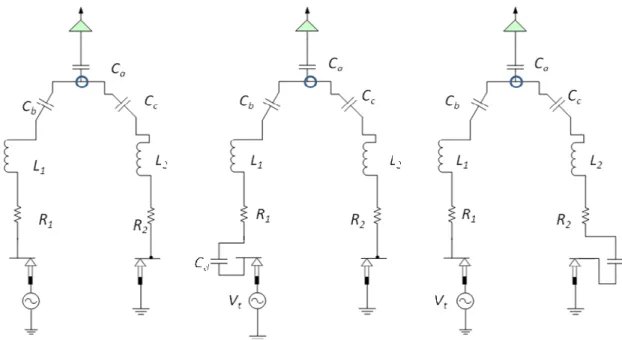
In fact, the Network Parameter Measurement used same fixtures as Capacitive Lead Frame Testing shown in Figure 2-3. In the connector circuit, there are normally series- equivalent-resistors, series-equivalent-inductors, and series-equivalent-capacitors on path from one pin to the other one. Sense capacitors exit between the high pin end and the sense plate. In addition, a mutual inductance exists between neighboring pins [2]. The relationship can be found between any neighboring pins. In Figure 2-4 simple equivalent circuit models are used to show the principle.
11 Csense2 R2 L2 L1 Ccouple Csense1 R1 Tester signal Ground Csense2 Ccouple Csense1 Copen Tester signal Ground R2 L2 L1 R1 (a) (b) (c)
Figure 2- 4. Equivalent circuit models with (a) non-defective pins (b) open defect on tested pin (c) open defect on neighboring pin [3]
In Figure2-4 above, difference among parts (a) (b) and (c) is the open-capacitance. When open capacitance exits in different position, the impedance seen from sense plate; the voltage / current signal sent to the buffer amplifier will all be changed. To make the
analysis more clear, the capacitors Csense1, Csense2and Csense3 with delta structure in Figure
2-4 is transferred to be Ca , Cb and Cc with Y structure in Figure 2-5. Cd is the defective
12
Figure 2- 5. Equivalent circuit model to neighboring pins with delta to Y transfer with (a) non-defective pins (b) open defect on tested pin (c) open defect on neighboring pin
The real values of the equivalent resistance, capacitance, and inductance can be obtained from the Agilent Pspice model. In the model, typical equivalent resistance value is around 0.0006 ohms, equivalent capacitance is about 0.002 pF and equivalent inductance is about 0.3 nH.
For example, consider the parameter set R1=0.6 mΩ R2= 0.6 mΩ L1=0.3 nH
L2=0.3 nH Csense1=0.002 pF Csense2=0.002 pF Csense3=0.002 pF and we set Vtest=2 V
f=8000 Hz 1 3 2 3 2 * sense snese sense sense sense a C C C C C C = + + (2.1) 2 3 1 3 1 * sense snese sense sense sense b C C C C C C = + + (2.2) 3 1 2 1 2 * sense snese sense sense sense c C C C C C C = + + (2.3)
13
The condition of the pin, i.e., no-open defect, open defect at tested pin, or open defect at neighboring pin changes the impedance measured across the tested pin, which
will lead to the change of voltage (Vo) in the fork point (the circled point in Figure 2-5).
The change of Vo will directly result in change of the current (Isig) flowing into the buffer
amplifier.
The voltage and current signal change in the three cases is illustrated with mathcad plot in Fig 2-6, Fig 2-7 and Fig 2-8.To simplify the description, the impedance of buffer is set to be zero here.
For non-defective connector:
b c a c a n C j L j R R L j C j C j R L j C j C j Z * * 1 * * ) * * * * 1 ( * * 1 ) * * * * 1 ( * * 1 1 1 2 2 2 2 ω ω ω ω ω ω ω ω + + + + + + + + ⋅ = (2.4)
Zn is the impedance seen from the signal generate into tested pin without defects.
(2.5) Then, a o sig C j V I * * 1 ω = (2.6) Vo =0.5V Isig =1.005e−10A When the pin under test opens:
* * * * 1 ( * * 1 ) * * * * 1 ( * * 1 * 2 2 2 2 R L j C j C j R L j C j C j Z V V c a c a n t o + + + + + ⋅ = ω ω ω ω ω ω
14 d b c a c a d d C j C j L j R R L j C j C j R L j C j C j C Z * * 1 * * 1 * * ) * * * * 1 ( * * 1 ) * * * * 1 ( * * 1 ) ( 1 1 2 2 2 2 1 ω ω ω ω ω ω ω ω ω + + + + + + + + + ⋅ = (2.7)
Zd1(Cd) is the impedance seen from the signal generate into tested pin with open solder defect at tested pin.
a d d t d o C j C Z V C V * * 1 * ) ( ) ( 1 1 ω = (2.8)
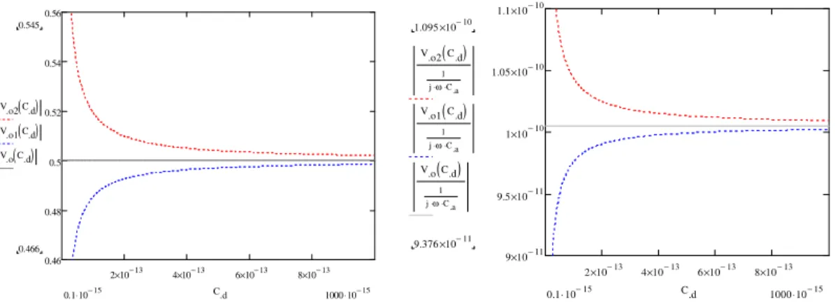
Since the parameter Cd is a variable in the formula above, we can use mathcad to plot
the relationship between Cd and the signal amplitude. As shown in Figure 2-6, voltage
and current signals all increase with the increase of Cd.
2 10× −13 4 10× −13 6 10× −13 8 10× −13 0.46 0.47 0.48 0.49 0.5 0.499 0.466 V.o1 C.d1( ) 1000 10⋅ −15 0.1 10⋅ −15 C.d1 2 10× −13 4 10× −13 6 10× −13 8 10× −13 9.2 10× −11 9.4 10× −11 9.6 10× −11 9.8 10× −11 1 10× −10 1.02 10× −10 1.002 10× −10 9.376 10× −11 V.o1 C.d1( ) 1 j⋅ω⋅C.a 1000 10⋅ −15 0.1 10⋅ −15 C.d1 (a) (b)
Figure 2- 6. Signal amplitude changes with Cdwhen the tested pin open (a) the voltage
amplitude at fork point (b) current amplitude flowing into the buffer
15 b d c a d c a d d C j L j R C j R L j C j C j C j R L j C j C j C Z * * 1 * * ) * * 1 * * * * 1 ( * * 1 ) * * 1 * * * * 1 ( * * 1 ) ( 1 1 2 2 2 2 2 ω ω ω ω ω ω ω ω ω ω + + + + + + + + + + ⋅ = (2.9)
Zd2(Cd) is the impedance seen from the signal generate into tested pin with open solder defect at neighboring pin.
+ + + + + + + ⋅ = ) * * 1 * * * * 1 ( * * 1 ) * * 1 * * * * 1 ( * * 1 * ) ( ) ( 2 2 2 2 2 2 d c a d c a d d t d o C j R L j C j C j C j R L j C j C j C Z V C V ω ω ω ω ω ω ω ω (2.10) 2 10× −13 4 10× −13 6 10× −13 8 10× −13 0.5 0.51 0.52 0.53 0.54 0.55 0.545 0.502 V.o2 C.d2( ) 1000 10⋅ −15 0.1 10⋅ −15 C.d2 2 10× −13 4 10× −13 6 10× −13 8 10× −13 1 10× −10 1.02 10× −10 1.04 10× −10 1.06 10× −10 1.08 10× −10 1.1 10× −10 1.095 10× −10 1.009 10× −10 V.o2 C.d2( ) 1 j⋅ω⋅C.a 1000 10⋅ −15 0.1 10⋅ −15 C.d2
Figure 2- 7. Signal amplitude change with Cdwhen the neighboring pin opens (a) the
voltage amplitude at fork point (b) current amplitude flowing into the buffer
In Figure 2-7, the voltage and current signal amplitude decrease a lot with the
16 2 10× −13 4 10× −13 6 10× −13 8 10× −13 0.46 0.48 0.5 0.52 0.54 0.56 0.545 0.466 V.o2( )C.d V.o1 C.d( ) V.o C.d( ) 1000 10⋅ −15 0.1 10⋅ −15 C.d 2 10× −13 4 10× −13 6 10× −13 8 10× −13 9 10× −11 9.5 10× −11 1 10× −10 1.05 10× −10 1.1 10× −10 1.095 10× −10 9.376 10× −11 V.o2 C.d( ) 1 j⋅ω⋅C.a V.o1 C.d( ) 1 j⋅ω⋅C.a V.o C.d( ) 1 j⋅ω⋅C.a 1000 10⋅ −15 0.1 10⋅ −15 C.d
Figure 2- 8. Combined signal amplitude change in the three situation (a) the voltage amplitude at fork point (b) current amplitude flowing into the buffer
Based on formulas above we could compare the three cases as can be seen in the three plots of Figure 2-8. Since there is no Cd in the non-defective situation, the signal
amplitude in the situation won’t change with Cd. That will result in the straight line in
grey color in Figure 2-8 (a) and (b). The red waveforms in Figure 2-8 (a) and (b) are signal amplitude with open tested pin, which is always higher than the non-defective signal amplitude. The blue waveform is the signal amplitude with open neighboring pin, which is always lower than the non-defective signal amplitude. Comparing the three waveforms in the Figure 2-8 (a), (b) we can see that open tested pin causes significantly lower signal amplitude, while the open neighboring pin can cause higher signal amplitude than the normal value.
With the three waveforms in the Figure 2-8 (a) we can also see that difference among
waveforms is large when Cd is small. In the plate capacitor
d A
Cd =ε* , where ε is the
dielectric constant, A the area of plate, d is the distance between two plates. Since the
17
Then, when the solder open is large enough, which would lead to a small open defective capacitance, the signal amplitude deviation from normal value will be clear.
The buffer in fact is a signal amplifier, which has an impedance value. If virtual ground wasn’t assumed at the buffer amplifier, we can assume constant amplifier
impedance Zamp connected to the upper end of Ca (Figure 2-5). Then Vsignal can be
calculated from voltage divider rule as:
amp a amp o signal Z C j Z V V + = * * 1 * ω (2.11)
The signal voltage has similar trend to that of Vo discussed previously.
In fact, the NPM is not limited to the grounded and power pins on connector. It can be applied to the signal pins as a subset of the capacitive Lead Frame Testing, which will explain the high abnormal readings in the test data in the following Chapters.
18
Chapter 3.
Principal Components Analysis Based Outlier Detection
Threshold settings such as relative thresholds based on standard deviation are used currently with capacitive testing to differentiate the normal values from the abnormal capacitance values. However, the shrinking size of the features and the resulting lower capacitance of signal pins make it more and more challenging to set such a threshold values. Non-optimal threshold settings can give rise to higher false fails or false passes. The challenge is further compounded due to the fact that each pin tested has a threshold that is different from others, yet often correlated to them. Furthermore, mechanical parameters such as spacing between the plate and the connector/device vary from one mounting on the tester to another. Similarly, the capacitance value corresponding to a pin may vary from board to board due to the fact that components are from different vendors. These and other factors combine to make the selection of appropriate thresholds a challenging task.
As an effective tool in this thesis we present a Principal Components Analysis (PCA) based technique to analyze the Capacitive Lead Frame test data and to detect defective boards,. PCA has been a well-known multi-dimensional correlated data analysis method for more than 100 years. PCA has been successfully applied to visualizing data, data exploration, outlier detection, compressing data etc. In electronic testing arena, PCA has been used to detect outlier Integrated Circuits [5][6].
In this Chapter, a background of the PCA will be provided, which includes the transformation formulae and test statistics for outlier detection.
19
3.1. Introduction to PCA
One of the best-known multivariate analysis methods, Principal Components
Analysis (PCA) was introduced by Pearson at the beginning of the 18th century. Then, it
was further developed by Hotelling in 1933[9].In Principal Components Analysis, a multi-dimensional interrelated data set is transformed to be a much lower dimensional data set while retaining as much of the information as possible. This kind of dimension reduction can be achieved by transforming the original data set into a series of uncorrelated Principal Components (PCs). In the series of PCs, data is ordered from high variance to low variance, where the first few PCs can contain the most information [9].
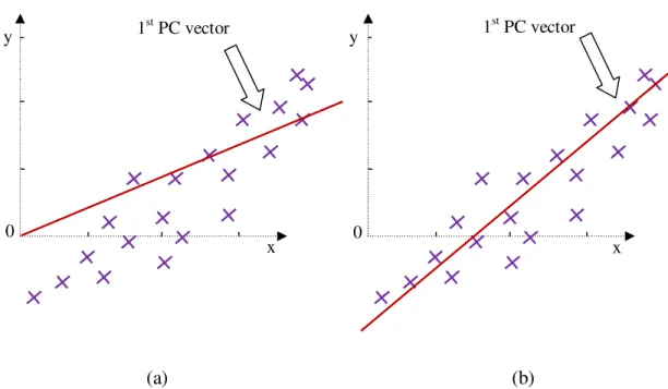
The PCA transformation can be specified by following steps: First, find the direction that achieves the largest projection variance from the data projection; After finding the direction above, we continue to look for another direction, which is orthogonal to that one and contains as much of the remaining variance from the data projection as possible. That is shown in Figure 3-1. Then, we look for the third one, and so on. In fact, the direction can be considered as the linear combinations of the original data set. The process continues until the remaining linear combinations or Principal Components are found.
The aim of the direction seeking is to capture the variability in the original data set [10]. Of course, the PCA should be applied to inter-correlated data. If no such correlation exists in the data, PCA representation won’t have an advantage over the original representation.
20
Figure 3- 1. Test observations with the first two Principal Components working as axis
3.2. Mathematical Representation of PCA
Let the Mm×n be the matrix of capacitance measurements, where m is the number of
boards, each with n measurements corresponding to the n tested pins. Let Mc be the
centered matrix where mean value of its column is subtracted from each element. The mean value of the column is the “measured capacitance of a pin averaged over all
boards”. For example the mean value of the ith column can be defined by
n M M M M i i ni i mean ) ... ( 1 2 _ + + + = (3.1)
where Mni is the nth component in the ith column.
With centered raw data matrix, there are two methods that may be employed to compute the Principal Components.
The first one, which is widely used in literature, involves computing the covariance matrix C of the centered matrix first:
0
1st PC vector
x y
21
C=Mc*McT (3.2)
Sometime the correlation matrix is also needed when data types inside the original matrix are much different from each other. The correlation matrix R is the normalized
covariance matrix such as C, in which element
n m mn mn S S C R = (3.3)
The Sm and Sn are square roots of variance to corresponding to column and row of
element (m,n). Cmn is the element (m,n) in covariance matrix C above [5].
After the above steps, PC calculation can be carried out by Eigen Value Decomposition (EVD): E=V*L*V−1 (3.4)
where E is either the correlation matrix R or the covariance matrix C. PC score can
be calculated from [5]
Z
=
M
cV
(3.5)The second approach applies Singular Value Decomposition (SVD) to the centered
real data matrix Mc. SVD technique computes U, S, V such that
T c USV
M = (3.6)
where the columns of U and V are called singular vectors, and S is the diagonal matrix containing the singular values [10][11][12][13]. In factorized style:
(
)
= = T n T T T r m T c u u u USV Mυ
υ
υ
δ
δ
δ
... ... ... ... ... 2 1 2 1 2 1 (3.7)22
In the Equation (3.7), ‘r’ is the rank of Mc. When r<m, other elements following δrT
are equal to 0.
The columns of U and V are called singular vectors. S is a diagonal matrix that contains the singular values. In outer-product form [10] it is:
T i i n i i c u M
∑
δ υ = = 1 (3.8)From the factorization above, the PC score or Z-score matrix Zm×n is given by
equation (3.5) where
Z
=
M
cV
Each board is now characterized by n PC scores or Z scores, represented by the ncolumns of Z. The first coordinate (called the first principal component) account for the
direction that contains most variance of data projection thenthe second one, and so on. In
fact, the variance of each column in the Z score matrix is automatically ordered by the algorithm from high to low. Figure 5-3 in Chapter 5 illustrates an example of Z score matrix. As can be seen, Z score variance values decrease from high to low along the column number.
In SVD, algorithm forces the first component to go through origin while maximizing
the variance projected. Use of the centered matrix Mc ensures that the first coordinate is
not forced to pass through the origin, and thus can catch the real maximum projected variance from the data [10][34][35][36]. Figure 3-2 shows an example of a PC plot in two-dimensional data. In Figure 3-2 (a), the largest Principal Component is calculated from non-centered dataset which starts from origin. As can be seen, this principal component doesn’t really catch the largest projected variance from data. When the PC is
23
calculated with centered data the largest PC will be the one expected. As shown in Figure 3-2 (b), start point of the first PC vector is not limited to the origin, and is able to capture the largest projected variance.
(a) (b)
Comparing the two methods EVD and SVD, SVD is the more robust, reliable and precise method with no need to compute the input covariance/correlation matrix. In numerical analysis fields, SVD is well known for its convergence and stability properties and it also works well with ill conditioned matrices [13]
3.3. Outlier Detection with PCA
Outliers are observations (test results of boards or connectors) that are numerically distant from the rest of the observations (of boards or connectors). In n-pin (n variables) test results, the outliers will be much different from the rest of the devices in the
n-0 0 1st PC vector 1st PC vector x y x y
Figure 3- 2. Comparison the first PC vectors calculated from (a) non-centered data and (b) centered data
24
dimensional space. In multivariate data, outliers can also be observations that never show extreme values in any one dimension. That is because of the general data structure (or plot trend) of outlier does not confirm with the rest of the observation. Such kind of outliers will not be detected by inspecting variables one by one [11].
Gnanadesikan and Kettenring (1972) discussed the plots that use only a few PCs to detect outliers. Such kind of plots (as shown later in Figure 5-4 and Figure 5-5) use the Principal Components as axes; represent the observations (devices) as scatter points to roughly show the outliers [11].
3.4. Test Statistics
To detect the outliers, i.e., boards or connectors with test measurement patterns that are significantly different from the rest of the boards or connectors, a distance measure is used. Since the variance of the first and last few PCs vectors contain different information, the first few PCs and last few PCs can detect different types of outliers. Different test statistics such as d1i, d2i, d3i and d4i have been defined which can be applied
for detecting different type outliers [11].
∑
+ − ==
q q p k ik iz
d
1 2 2 1 (3.9)The calculation of statistic d1i2 (suggested by Rao [11]) is based on the Principal
Components. If there is no outlier, the independent observations d1i (d1i = d12i ) should
follow a Gamma distribution.In the formula of d1i,Zik is the value of the kth PC for the ith
board; p and q define the sequence numbers of the first and last PC used for the
25
∑
+ − ==
p q p k k ik il
z
d
1 2 2 2 (3.10)A weakness of d1 is that it gives insufficient weight to the last few PCs, especially
when the one with large variance and the one with very small variance are used together. So d2i was proposed in [11] as an alternative to d1i. The PCs inside of d1iare normalized
by the variance of its column. In the d2i formula above, lk is the variance of the kth PC.
Gnanadesikan and Kettenring [11] also use the d3i as test statistics. d3i can detect
outliers in the data with large effect on first few PCs.
∑
==
p k ik k il
z
d
1 2 2 3 (3.11)Hawkings also defined a d4i statistic that works effectively in many experiments
[11]. k ik p k q p i
l
z
d
≤ ≤ + −=
1 4max
(3.12) In some literatures,∑
= = p k k ik i l z d 1 2 20 [8] (3.13), and log10( max )
1 k ik p k q p i l z X ≤ ≤ + − = [4] (3.14)
are also used as test statistics. As can be seen, d0i is very similar to the square root of d2i,
except its p and q are set to be the same value. The Xi value could be viewed as the
26
The four di statistics presented above have been suggested for outlier detection with
Principal Components [11]. Using the information of several PCs (subset of the Z score matrix), all of them can change the multivariate analysis into single-variable analysis.
Since the first and last few PC vectors contain different information, the first few PCs and last few PCs can detect different types of outliers [11]. The best test statistics for a given problem depends on the data type and the purpose of the test.
The basic concept for PCA based test technique was described above. We use two different schemes based on the same technique for testing the PCBs. First, we use a
global method, which uses the entire data set for the board to identify outliers. In this
case, the PCA based algorithm would be applied to the whole measurement matrix. This method takes into account the variations such as tester to tester variation or fixture to fixture variation more effectively as effect of such variations manifest over the entire set of measurements. However, a weakness of this method is the fact that an open in one pin influences the capacitance values of only few other pins in its neighborhood. Thus the overall effect on the test statistic is like to be somewhat smaller, as the analysis is based on the dataset for the entire set of pins.
Therefore in localized method, we propose an outlier detection scheme based on a
small window of pins at a time. The original measurement matrix M is first sorted according to the pin number in relative physical layout area. Then the matrix is first vertically separated into different smaller matrices (test windows). A calculation similar to that in global analysis is applied to each window. To cover the entire connector or the set of pins, the test is performed by carrying out the evaluation in each window to cover the entire set of pins, one window at a time. Thus we have two options, overlapping
27
windows or non-overlapping windows. We will address the global and localized method in detail in Chapters 5,6,7,8.
28
Chapter 4
PCB Test Data Sources
This chapter introduces the test background and datasets of PCB measurements used in this work. Section 4.1 provides the background for board testing. Then the dataset used for further analysis in later chapters is illustrated in Section 4.2.
4.1. Background for Boards Test
Some of the defects that may be introduced during board manufacture include the following: opened solder; insufficient, excess or malformed solder joints; missing devices; shorts which can be caused by device mis-registration; excess solder; dead devices; incorrect device placement; polarized devices wrongly placed; and misaligned parts [1]. To ensure that the boards are defect-free before they are shipped to customers, different types of tests are applied to detect such defects. The different board test steps are discussed next.
Structural tests, functional tests and system tests are used for board testing. As is shown in Figure 4-1, these test steps are employed one by one after the manufacture. The following paragraphs will introduce these steps in detail.
29
Loaded Board Inspection is a test step that applies some operation wave such as
X-ray to illuminate the area of interest and capture an image. By comparing the image with specifications, the quality of the device under inspection can be judged. Loaded Board Inspection includes Automatic Optical Inspection (AOI) and Automatic X-ray Inspection (AXI). AOI and AXI use two different operation wavelengths, visible light and X-ray illumination. AOI does not utilize penetrating radiation. The light illuminates the board from different directions. Then the radiation is reflected from the exposed board surface. If the part cannot be illuminated, it cannot be tested. AXIon the other hand can detect the
Board manufacture
Structural Test
Functional Test
System Test
Failure Analysis
Loaded Board Inspection30
inner parts of objects like copper, board materials and integrated circuits. Both 2-dimensional and 3-2-dimensional inspection can be achieved by AXI. Two-2-dimensional test is simpler but the image suffers from the degeneration of resolution when there are components on both sides of the board. This problem can be solved by 3-dimesional tests, but at the cost of more mechanical complexity [1, 21].
Different from other tests, Loaded Board Inspection doesn’t need much programming information. However, it can find the defects that cannot be found by ICT such as the alignment and solder quality problems.
Structural Test is the test step that inspects the internal board structure to ascertain
whether the board is built correctly. It is able to identify defects such as wrong components, incorrectly installed components and missing components. Structural tests includes In-Circuit-Test (ICT) and Boundary Scan. ICT utilizes electrical probes to test PCBs for defects such as opens. Most of the time it is a low frequency test technique. During the test, the board is not operated as it is normally intended to [1]. ICT employs unpowered and powered test.
With Unpowered test the whole PCB doesn’t need to be activated, i.e., powered on, during the test. Signals may be applied only to the part under test to obtain responses. For testing a short in a specific component, for example, a load resistor in series with a small voltage source is connected. Then a limited voltage or current stimulus is applied to the part under test. Since the voltage across the load resistor will be monitored, once the voltage exceeds a threshold voltage, a short defect may be considered to exist [1].
When the unpowered tests are applied to PCB components such as resistors, inductors and capacitors, which have associated nominal values and a tolerance, the
31
unpowered test is also termed as ‘unpowered analog test’ to measure these component values. Finding open signal pins on connectors or ICs with Capacitive Lead Frame testing and Network Parameter Measurement (NPM) are examples of unpowered analog tests.
Powered In-circuit Digital Test is a test employing a digital sequencer to test digital devices such as ICs on the boards. Digital input signals are applied to the devices while monitoring digital responses at the same time. In practice, there may be several similar processes running at the same time.
Programmable analog parameters such as voltage, slew rate, and receiver high/low voltage comparison windows are needed for drivers and receiver / comparator circuits.
Powered In-circuit Digital Test also needs to utilize lots of memory to store digital stimulus, response [1].
Powered Mixed-signal Test is a test used when both analog and digital test are needed. The digital subsystem and analog subsystem on the In-Circuit tester can coordinate the tests in this case. For example, to test a Digital-to-Analog converter on a board, the digital subsystem may simulate digital data corresponding to a sine wave, while the analog subsystem measures the frequency or distortion of the signal.
In-circuit-test is effective in detecting the presence, correctness, orientation, liveness (whether the component is ‘dead’), shorts and open defects. Since the visual inspection can only determine whether the device is present and appears correct, it cannot tell if the device is dead or defective. In-circuit-test can apply electrical tests to these components. However, ICT is essentially useless for detecting defects associated with device alignment and joint quality [1]. The In-Circuit-Test steps for printed-circuit boards are presented in Figure 4-2.
32
ICT has fast test speed, provides good defect detection at component level and facilitates automatic test development. However, ICT has a high cost and may cause high board stress due to high probe density.
4.1.1.1. Functional Test is a test check
Boundary-Scan Tests is a method to test PCB wire lines or IC sub-blocks without applying physical probes. During the test, build-in Boundary-Scan devices in digital ICs are utilized to perform testing. When not used, these circuits and devices turn back to normal functions.
Normally, Boundary-Scan Tests can also be considered as a subset of Design-For-Test rules, which will facilitate the board testing [1, 31]. The specifications in IEEE STD
Manufactured Board
Place on fixture and activate fixture
Unpowered Short Test
Remove and Repair Fail?
Unpowered Analog Test
Powered Digital Test /Mixed Signal Test
Ship to Next Test Step Fail? No Yes No Yes Turn on power
Turn off power
33
1149.1[1] developed by the Joint Test Action Group (JTAG) for Boundary-scan, Boundary-scan test describes this semi-automated and fast test method. It also requires minimum test access, which helps the board testing when test probes are compromised by the layout density. Defects such as opens and shorts in digital ICs can be detected by this method [1,22-26].
Functional Test is a test to confirm that a board meets its design criteria. The board
under the test needs to operate toward its original design purposes on a test platform for verifying its performance specification. A board that passed the structural tests may not pass the Functional Test step [4, 31].
Normally, the functional test has to and is capable of providing very good test coverage. However, it cannot provide good diagnostics; in other words, it is not able to tell the exact defects or the defect locations. Functional tests need a long test time and a costly design effort [32].
System Test is a type of test where the boards are inserted into the final system and
then the system is turned on to see if the whole system works well with the product. This test can only give pass/ fail but can’t give detailed defect information [1].
In the practice, most of the tests above will collaborate to filter the bad boards. In modern test systems, the total test time for all of the tests above may only last 30 to 50 seconds.
4.2. PCB Measurements Datasets
This thesis uses Capacitive Lead Frame Test (called TestJet in industry) data for several different PCBs obtained using Agilent testers. When performing TestJet
34
measurements, the tester uses relays to connect the board pin under test to an AC source running at 8192 Hertz and around 250 mV peak-to-peak. The voltage is so low that it minimizes the chance of diodes on the board turning on. All the pins except for the pin-under-test are connected to the ground.
The sense plate transfers the signal to a buffer amplifier and then to a signal analyzer, which detects the capacitances in femto-farads scale with sensed signal. The sensor may get an average value over several periods of AC signal.
Measurements in the test dataset we use correspond to connectors residing on boards tested in a working production line. For each connector on the board, all but the grounded/VDD pins were tested and capacitance measurements obtained. A board could be tested more than once to test the repeatability, so there can be multiple data records for a single board (each record is termed as a boardrun).
35
Dataset Name # of Connectors
in data Tested Pins
Boards Measurement D0 5 670 22 J24 1 145 15 J25 1 150 15 J27 1 147 15 J28 1 151 15 J31 1 77 22 D1 7 1053 20 J7 1 132 20 J10 1 132 20 J13 1 133 20 J16 1 131 20 J41 1 130 20 J45 1 133 20 J47 1 129 20 J50 1 133 20 D3 4 594 83 Data3_j24 1 145 83 Data3_j25 1 150 83 Data3_j27 1 148 83 Data3_j28 1 151 83 LVLD1 2 262 6 J3_norm 1 142 6 J10_norm 1 120 6 LVLD2 2 262 5 J3_all 1 142 5 J10_all 1 120 4 LVLD3 2 262 4 J3_projection 1 142 4 J10_projection 1 120 4 LVLD4 2 262 4 J3_all 1 142 4 J10 all 1 120 4
36
D0, D1, D3, LVLD1, LVLD2, LVLD3, LVLD4 identify seven different datasets used in this thesis. For each dataset, there may have several different connector measurements. For example, in dataset D1, the data in Data3_j24 and Data3_j27 are from connector j24 and j27.
In each test dataset there are some unique tested boards. When needed, some boards have been tested several times. We call each measurement set corresponding to one set of measurements of a board as a boardrun. Thus the same board may be associated with multiple board runs. Datasets in D3 are composed of four different types of connector test measurements. Each dataset measurement contains 47 unique boards. However, some boards were tested multiple times resulting in the 83 board measurements termed as boardruns in the following.
D1, a relatively comprehensive set, includes 17 unique boards with a total of 20 boardruns. Each of the board in Data_D1 includes eight connectors: j7, j10, j13, j16, j41, j45, j47 and j50.The multiple connectors lead toover 1000 pins tested per board.
Data in LVLD1, LVLD2, LVLD3 and LVLD4 all contain measurements of connectors j3 and j10, which are DDR2 memory card connectors. However, j3 on this particular board is mounted at a 45 degree angle, i.e., the board that is plugged in will be at a 45 degree angle to the main board. J10, like other connectors, is perpendicular to the board. For example, Data_j3 is from j3 connector and corresponds to 6 unique boards.
The four measurement datasets in D0, namely j24, j25, j27 and j28 are based on the tests for 240-pin DDR memory card connector. However, j30 is a 140-pin connector. The test data sets described above will be used for the analysis in the following chapters. All of the datasets were provided by Agilent Technologies.
37
Chapter 5.
PCA Analysis of Board Measurements with d Statistics
This chapter illustrates the use of the PCA based outlier detection approach.
Different test statistics are applied to data sets Data3_j24 and Data_D1. In Section 5.1,
dataset Data3_j24 is introduced and analyzed to investigate the effectiveness of PCA.
Then in Section 5.2 different test statistics based on PCA are applied. To make the
comparison between test statistics clearly, different subsets of most-significant and
least-significant PCs are used. To support the conclusion drawn in Section 5.2, Section 5.3
applies the method to another dataset Data_D1. Selection of test statistic parameters is
also discussed.
5.1. Analysis of Measurements of a Single Connector with Principal Components
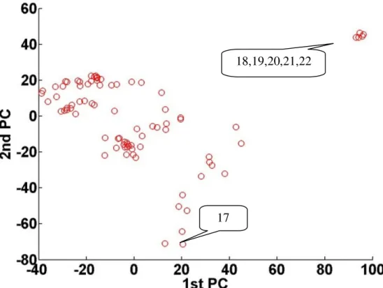
Figure 5-1 is the plot of 83 boardruns for Data3_j24 while Figure 5-2 shows these
same measurements with clear outliers removed. As can be seen from Figure 5-1, while
the general pattern remains the same, the measurement variation among different
boardruns is often detectable. The six boardruns 17, 18, 19, 20, 21, 22 would be
identified as outliers by manual inspection of data. Of course there are other outlier
boardruns besides the six above that are harder to identify (e.g., boardruns 4, 5, 14,
15……). Figure 5-2 shows the same data, but without the six outliers. Test results for
pins 210 to 240 (the right part of plot) have a significantly higher variation compared to
the others. A close inspection of the plots for different boards shows strong fluctuations
38
Figure 5- 1. Plot of raw measurements of Data3_j24
Figure 5- 2. Plot of raw measurements of Data3_j24 with outliers removed 17
18, 19, 20, 21, 22 18, 19, 20, 21, 22 4,5
39
To present the point clearly here, boardrun 17 and boardruns 18, 19, 20, 21, 22
would be used as clear outliers, which can be inspected from the difference between
Figure 5-1 and Figure 5-2.
5.1.1. PCA Result for Data3_j24
Principal Components can be utilized for outlier detection. The Principal
Components are calculated with centered SVD algorithm. The calculated Z score matrix
contains PC vectors. 0 200 400 600 800 1000 Z S c o re V a ri a n c e
PC Number
Figure 5- 3. Plot of Z score variance values for Data3_j24
Figure 5-3 shows the variance of the Z score values with PC numbers. As can been
seen, variance of the Z score values change gradually from largest variance to a minimal
one with the PC number. Since the first and last few PCs contain different information,
40
To test the effectiveness of PCA for identifying outliers, we use a series of scatter
plots of different combinations of PCs vectors. With first two PCs vectors as x-axis and
y-axis respectively, boardrun number has been plotted according to these values in Figure
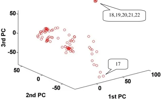
5-4. In the figure, boardruns 17, 18, 19, 20, 21, 22 are relatively far away from the cluster
of other devices. Similar phenomenon can also be detected in the 3-Dimensional or
higher dimensional plots. For example, in Figure 5-5, an additional PC vector, the third
PC vector, works as the z-axis.
Figure 5- 4. Boardruns plot for Data3_j24 with the first two PCs as axes 18,19,20,21,22
41
Figure 5- 5. Boardruns plot for Data3_j24 with the first three PCs as axes
From the two plots above, clear outliers like 17, 18, 19, 20, 21 and 22 could be
observed as clearly different from the others, which means Principle Components appear
to be effective in multi-dimensional outlier detection. However, the scatter plot analysis
above is based on inspection. The multi-dimensional analysis can be reduced to a
one-variable analysis with test statistics such as d1, d2 d3, and d4.
Calculation of test statistics d1, d2, d3, d4, with given Principal Components is applied
to all of the boardruns in Data3_j24. Then the boardruns are sorted according to the
respective test statistic value (d value). Since the Cumulative Distribution Function
(CDF) plot can clearly show the difference between the test statistics value with boardrun
numbers, all of the boardruns are plotted onto the CDF curve with respect to their own 18,19,20,21,22
42
test statistics values. The outlier boardruns would stand out at the high-end of the CDF
curve.
5.2. Selections of Test Statistics and PCs
In this section, we investigate the selection of appropriate PCs for outlier detection in
PCBs. The set Data3_j24 is tested with four different test statistics using different
combinations of PCs.
5.2.1. ‘d’ Statistics with Most Significant PCs
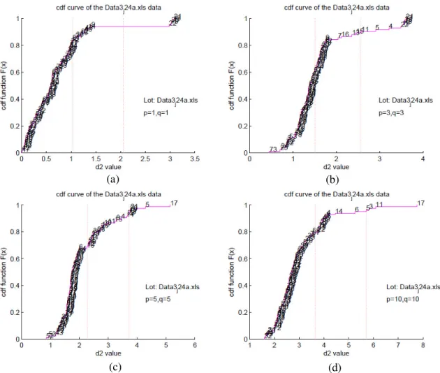
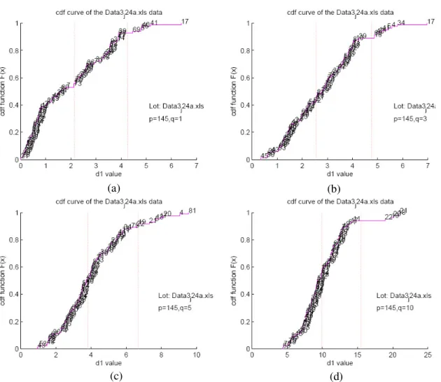
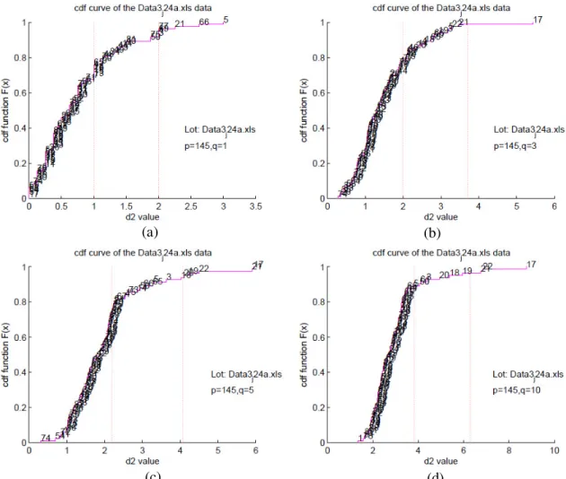
In the following analysis the four test statistic are evaluated and compared with the
most significant 1, 3, 5, 10 PCs respectively. .
In Figure 5-6, d1 value is represented on x-axis, six clear outliers, namely 17, 18, 19,
20, 21, and 22, stand out at the high end of the CDF curves. The clear break after the six
devices number shows that these six boardruns are far away from the other devices in the
multi-dimensional test result. Some other boardruns after the clear break like 15, 14, 5, 4,
13, 11, 16, 8, 9 and 10 can also be grouped as potential outliers.
CDF plots in d2 and d4 scale are somewhat similar. In d2 CDF curve (Figure 5-7), the
six boardruns only appear at the high end when the first PC is used. In the other 3
situations, boardrun 4, 5 show even higher d2 values than the boardruns 18, 19, 20, 21,
22. In addition, the break after device 18, 19, 20, 21, 22 is not clear enough to separate
them from others. The boardrun numbers sorted in d4 scale only match the inspection
result when the first PC is used, as shown in Figure 5-8 (a). However, the break after the
43
outliers to be undetectable. Analysis with the first 3, 5, 10 PCs give boardruns 5 and 17
higher d4 values than boardrun 18, 19, 20, 21, 22 do.
Figure 5- 6. CDF plot to all boardruns in d1 scale with (a) Only the first PC is used (b)
Only the first three PCs are used (c) Only the first five PCs are used (d) Only the first ten PCs are used
The boardruns circled are 17, 18, 19, 20, 21 and 22.
(a)
(c)
(b)
44
Figure 5- 7. CDF plot to all boardruns in d2 scale with (a) Only the first PC is used (b)
Only the first three PCs are used (c) Only the first five PCs are used (d) Only the first ten PCs are used (a) (c) (b) (d)
45
Figure 5- 8. CDF plot to all boardruns in d3 scale with (a) Only the first PC is used (b)
Only the first three PCs are used (c) Only the first five PCs are used (d) Only the first ten PCs are used
(a)
(c)
(b)
46
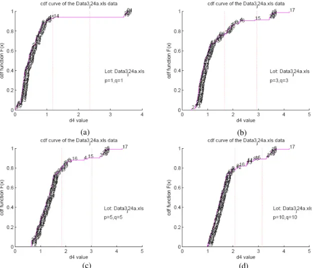
Figure 5- 9. CDF plot to all boardruns in d4 scale with (a) Only the first PC is used (b)
Only the first three PCs are used (c) Only the first five PCs are used (d) Only the first ten PCs are used
According to the sorting results in Figure 5-8, all of the plots using d3 give very
similar and matched results. This test statistic was also discussed in [11].
(a)
(c)
(b)
47
5.2.2. ‘d’ Statistics with Least Significant PCs
Figure 5- 10. CDF plot to all boardruns in d1scale with (a) Only the last one PC is used
(b) Only the last three PCs are used (c) Only the last five PCs are used (d) Only the last five PCs are used
(a)
(c)
(b)
48
Figure 5- 11. CDF plot to all boardruns in d2 scale with (a) Only the last one PC is used
(b) Only the last three PCs are used (c) Only the last five PCs are used (d) Only the last five PCs are used
(a)
(c)
(b)