Basic Principle of Buck-Boost
The buck-boost is a popular non-isolated inverting power stage topology, sometimes called a step-up/down power stage. Power supply designers choose the buck-boost power stage because the required output is inverted from the input voltage, and the output voltage can be either higher or lower than the input voltage. The input current for a buck-boost power stage is discontinuous, or pulsating, because the power switch (Q1) current that pulses from zero to IL every switching cycle. The output current for a buck-boost power stage is also discontinuous or pulsating because the output diode only conducts during a portion of the switching cycle.
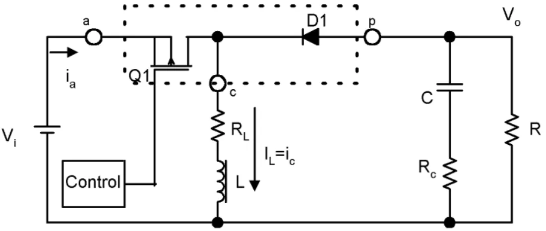
Figure 1 shows a simplified schematic of the buck-boost power stage. Inductor L and capacitor C make up the effective output filter. The capacitor equivalent series resistance (ESR), RC, and the inductor dc resistance, RL, are included in the analysis. Resistor R represents the load seen by the power supply output. The diode D1 is usually called the catch diode, or freewheeling diode.
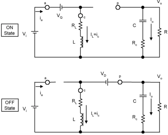
Figure 2. Buck Power Stage States The inductor current increase during the on state is given by:
The quantity ∆IL(+) is the inductor ripple current.
The inductor current decrease during the off state is given by:
The quantity ∆IL(-) is also the inductor ripple current.
In steady conditions, the current increase, ∆IL(+) and the current decrease ∆IL(-) must
be equal. Solving for VO:
) 1 ( . . . ) ( ) ( i Q L L ON L T L R I V V I + = − + × × ∆ ) 2 ( . . . ) ( ) ( O d L L OFF L L T R I V V I − = − − − × × ∆ ) ( ) ( − × − − × × + − = T T T R I V T T V V V OFF OFF ON L L d OFF ON Q i O
A common simplification is to assume VQ, Vd, and RL are small enough to ignore. Setting VQ, Vd, and RL to zero, the above equation simplifies considerably to:
Unlike the buck power stage, the average of the inductor current is not equal to the output current. To relate the inductor current to the output current, referring to Figures 2 and 3, note that the inductor delivers current to the output only during the off state of the power stage. This current averaged over a complete switching cycle is equal to the output current because the average current in the output capacitor must be equal to zero. ) 4 ( . . . . . 1 D D V VO i − × − =
Figure 4. Boundary Between Continuous and Discontinuous Mode
Further reduction in output load current puts the power stage into discontinuous current conduction mode(DCM). The discontinuous mode power stage input-to-output relationship is quite different from the continuous mode.
Figure 5. Discontinuous Current Mode
The duration of the on state is TON=D×TS, where D is the duty cycle set by the
control circuit. The duration of the off state is TOFF=D2×TS. The idle time is the
remainder of the switching cycle and is given as TS-TON-TOFF= D3×TS. These
times are shown with the waveforms in Figure 5.
The inductor current increase during the on state is given by:
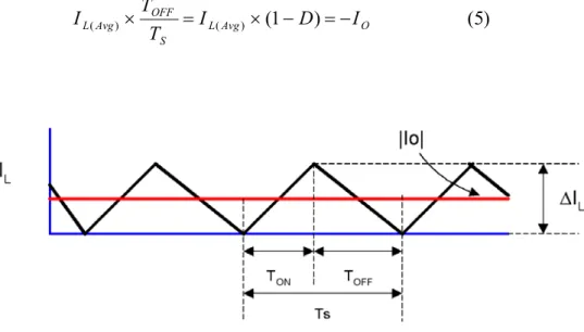
) 5 ( ) 1 ( ) ( ) ( LAvg O S OFF Avg L I D I T T I × = × − =− V V
The inductor current decrease during the off state is given by:
As in the continuous conduction mode case, the current increase, ∆IL(+), during the
on time and the current decrease during the off time, ∆IL(-), are equal. So,
) 7 ( 2 ) ( O S OFF O L D T L V T L V I − = − × =− × × ∆ ) 8 ( 2 D D V T T V V i OFF ON i O =− × =− ×
Now calculate the output current. It is the average over one switching cycle of the inductor current during the time when D1 conducts(D2*Ts).
Now solve two equations, IO and VO (equation 8 and 10), the discontinuous conduction mode buck voltage conversion relationship is given by:
Where K is defined as:
) 9 ( 2 2 1 ) ( × × = = = PK S S O avg L O D T I T R V I I ) 10 ( 2 2 2 ) ( ) 1 ( 2 1 1 L T D D V T D T D L V T R V I S i S S i S O O × × × × − = × − × × × × × = = K D V VO =− i × S T R L K × × = 2 ) 11 ( K M D=− × ) 12 ( i O V V M =
Critical Inductance
The previous analyses for the buck-boost power stage have been for continuous and discontinuous conduction modes of steady-state operation. The conduction mode of a power stage is a function of input voltage, output voltage, output current, and the value of the inductor. A buck-boost power stage can be designed to operate in continuous mode for load currents above a certain level usually5 to 10% of full load. Usually, the input voltage range, output voltage, and load current are defined by the power stage specification. This leaves the inductor value as the design parameter to maintain continuous conduction mode.
The minimum value of inductor to maintain continuous conduction mode can be determined by the following procedure.
First, define IOB as the minimum output current to maintain continuous conduction mode, normally referred to as the critical current. This value is shown in Figure 4. In boundary between CCM and DCM,
On Boundary: CCM: ) 1 ( 2 D I I I L OB LB =− − ∆ = ) 15 ( 2 ) ( 2 OFF L L d O ON L L O i LB T L R I V V T L R I V V I × × × − − − = × × × − − = ) 16 ( ) ( 2 2 ) ( 2 (max) 2 (max) (min) (max) min i o i OB S O ON LB L L Q i V V V I T V T I R I V V L − × × × − = × × × − − ≥ ) 13 ( ON L L Q i L T L R I V V I = − − × × ∆ ) 14 ( 1 D D V Vo i − × − =
Output Capacitor
In switching power supply power stages, the function of output capacitor is to store energy. The output capacitance for a boost power stage is generally selected to limit output voltage ripple to the level required by the specification. The series impedance of the capacitor and the power stage output current determine the output voltage ripple. The three elements of the capacitor that contribute to its impedance (and output voltage ripple) are equivalent series resistance (ESR), equivalent series inductance (ESL), and capacitance (C). The voltage variation due to the inductor current flow in the output capacitor is approximately:
For CCM Mode: For DCM Mode ) ( 2 2 IN d O PK O V V V C L I V − + × × × = ∆ O S O V f D I C ∆ × × ≥ max max o s s O V f T R L I C ∆ × × × − × ≥ 2 1 (max)
The above equation is based on the assumption that all inductor ripple current flows through the capacitor and the ESR is zero. Now, assuming that the capacitor is very large, the ESR needed to Limit the ripple to ∆VOmax is:
For CCM Mode:
For DCM Mode:
*The output filter capacitor should be rated at least 10~20 times the calculated capacitance and 30 to 50 percent lower than the calculated ESR.
The RMS value of the ripple current flowing in the output capacitance(CCM) is given by: PK O O Max O O I V I D I V ESR max (max) max ) 2 1 ( ∆ = ∆ + − ∆ ≤ PK O O O I V I V
ESR max = ∆ max
∆ ∆ ≤ D D I ICRMS O − × = 1
Buck-Boost DC/DC Converter Small Signal Model (Transfer Function):
) 1 ) ( ( ) ( ) 1 ) ( ( ) ( ) 1 ( 1 ) ( ) ( T s Z s i T s GV s V T T H s V s V OUT load g g ref O = + + + − + ∧ ∧ ∧ ∧ gain loop V s GV s G s H s T M d C = = ( ) ( ) ( ) ) (
For CCM Mode:
*Two Pole fLC , One Zero fESR for GVd(s) and One Right-Half-Plane zero
z From a practical view, at RHP zero frequency, the loop gain starts increasing at a 20dB/decade rate but the loop phase decreases by –45 degrees (in a normal, LHP zero, the loop phase will increase by +45 degrees). This imposes the restriction that the gain be rolled off to 0dB before encountering the RHP zero.
z The output inductor, capacitor and the capacitor’s ESR must be selected so that the double pole occurs first and then the output capacitor zero and then the RHP zero. This assures that the loop gain crosses 0dB at a slope that is first order (20dB/decade) and that the instability inherently associated with the RHP zero is circumvented by crossing 0dB before the RHP zero frequency occurs.
(
)
+ + − + − = 2 0 0 2 1 2 1 1 1 1 ) ( w s Q w s w s w s D V s GV g Z Z d C L R D Q≈(1− )× LC D R R D R LC w 1 L (1 )2 (1 ) 0 − ≅ − + = C R w C Z 1 1 =(
)
DL R D L R R D w L Z 2 2 2 ) 1 ( 1− − ≅ − = Compensate rule:For DCM Mode: + × × × × − = P S g d w s L T R V s GV 1 1 2 ) ( C R wP × = 2
Application Example of Buck-Boost Circuit
2 (max) 2 (max) (min) (max) min ) ( 2 2 ) ( i o i OB S O ON LB L L Q i V V V I T V T I R I V V L − × × × − = × × × − − ≥
VIN=5V, Vo=-8V,Io=100mA, fosc=500kHz
1. Inductor L1:
The condition of L because of a continuous current in the range of the use voltage
Select L=22µH, Load current value which becomes continous current condition.
If IO≥IOB, the peak value of the inductor IL(peak)
2. P-MOSFET Drain Current: Peak value
The peak value of the drain current of P-MOSFET should be in the rated current value of P-MOSFET. The peak current of P-MOSFET is assumed to be ID, ID is obtained by the following formula.
L t V D I I D I I O L O i ON peak L × × + − − = ∆ + − − = 2 1 2 1 ) ( A I IL L peak 0.399 10 22 2 10 2 615 . 0 0 . 5 615 . 0 1 1 . 0 6 6 ) ( × × = × × × + − = ≥ − − H V V V I T V L i o i OB S O 11.83µ ) 5 8 ( 5 1 . 0 2 10 2 8 ) ( 2 2 2 6 2 (max) 2 (max) min × × − − = × × = − × × × − ≥ − mA V V V L T V I i o i S O OB 53.79 ) 5 8 ( 5 10 22 2 10 2 8 ) ( 2 2 2 6 6 2 (max) 2 (max) min = − − × × × × × = − × × × − ≥ −− % 5 . 61 5 8 8 = − − − = − = i O O V V V D A I ID L peak 0.399 10 22 2 10 2 615 . 0 0 . 5 615 . 0 1 1 . 0 6 6 ) ( × × = × × × + − = ≥ − −
Where tr and tf are the MOSFET turn-on and turn-off switching times QGate is the MOSFET gate-to-source capacitance
3.Diode D1:
The peak value of diode current IFSM
The Average Current IF
The repetition peak reverse voltage of the diode VRRM
A I IF ≥ O ≥0.1 V V V VRRM ≥ i − O ≥11 s GS Gate s f r O o i ON DS O Q D t t f Q V f D I V V D R D I P × + × + × × − × − × + × × − = ( ) 1 ) ( 2 1 1 ( ) 2 ) 1 ( A I IFSM L peak 0.399 10 22 2 10 2 615 . 0 0 . 5 615 . 0 1 1 . 0 6 6 ) ( × × = × × × + − = ≥ − −
Basic Principle of Flyback
The flyback converter is based on the buck-boost converter. Its derivation is illustrated in Fig.7. Figure 7(a) depicts the basic buck-boost converter, with the switch realized using a MOSFET and Diode. In Fig. 7(b), the inductor winding is constructed using two wires, with a 1:1 turns ratio. The basic function of the inductor is unchanged, and the parallel windings are equivalent to a single winding constructed of larger wire.
In Fig. 7(c), the connections between the two windings are broken. One winding is used while the Q1 conducts, while the other winding is used when diode D1 conducts. The total current in the two windings is unchanged from circuit of Fig. 7(b); the current is now distributed between the windings differently. The magnetic fields inside the inductor in both cases are identical. Although the two-winding magnetic device is represented using the same symbol as the transformer, a more descriptive name is “two-winding inductor”. This device is sometimes also called a “flyback transformer”. Fig. 7(d) illustrates the usual configuration of the flyback converter.
Figure 8. Flyback converter with transformer equivalent circuit model The behavior of most transformer-isolated converters can be adequately understood by modeling the physical transformer with a simple equivalent circuit consisting of an ideal transformer in parallel with the magnetizing inductance. The magnetizing inductance must then follow all of the usual rules for inductor; in particular,
The magnetizing inductance LM functions in the same manner as inductor L of the original buck-boost converter of Fig. 7(a). When Q1 conducts, energy from the Vi is stored in LM. When the diode D1 conducts, this stored energy is transferred to the load, with the inductor voltage and current scaled according to the 1:n turns ratio.
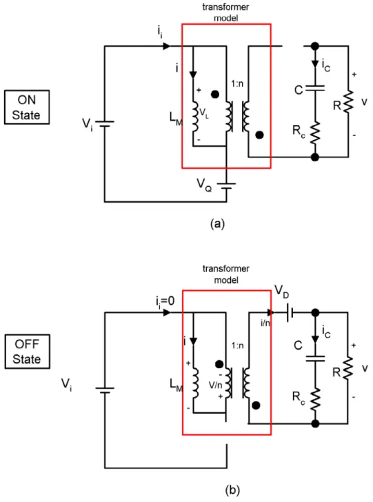
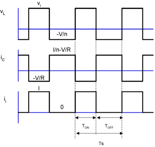
During on state, while Q1 conducts, the converter circuit model reduces to Fig. 8(a). The inductor voltage VL, capacitor current iC, and the DC source current ii, are given by
With the assumption that the converter operates with small inductor current ripple and small capacitor voltage ripple, the magnetizing current I and the output capacitor voltage v can be approximated by their dc components, I and V, respectively. Equation (17) then becomes
During off state, the equivalent circuit of Fig. 8(b) is obtained. The primary-side magnetizing inductance voltage vL, capacitor current iC, and the DC source current ii, are given by ) 17 ( i i R v i V v g C i L = − = = ) 18 ( I i R V i V v g C i L = − = = − = − = L v i i n v v
The vL(t), iC(t), and ii(t) waveforms are sketched in Fig. 9.
Figure 9. Flyback converter waveforms, CCM mode
Application of the principle of volt-second balance to the primary-side magnetizing inductance yields ) 20 ( 0 = − = − = g C L i R V n I i n v v
Solution for the conversion ratio then leads to
So the conversion ratio of the flyback converter is similar to that of the buck-boost converter, but contains an added factor of n.
Application of the principle of charge balance to the output capacitor C leads to
Solution for I yields
This is the dc component of the magnetizing current, referred to yhe primay. The dc component of the source current ii is
) 22 ( 1 ) ( D D n V V D M i − = = ) 23 ( ) ( ) 1 ( ) ( R V n I D R V D iC = × − + − × − ) 24 ( ) 1 ( D R nV I − = ) 25 ( ) (I D i Ii = i = ×
An equivalent circuit which models the dc components of the flyback converter waveforms can be constructed. The resulting dc equivalent circuit of the flyback converter is given in Fig. 10. It contains a 1:D buck-type conversion ratio, followed by a (1-D):1 boost-type conversion ratio, and an added factor of 1:n, arising from the flyback transformer turns ratio.
Effect of transformer leakage inductance
The peak MOSFET voltage is equal to the dc input voltage Vi plus the reflected load voltage V/n; in practice, additional voltage is observed due to ringing associated with the transformer leakage inductance. A snubber circuit may be required to clamp the magnitude of this ringing voltage to a safe level that is within the peak voltage rating of the MOSFET.
z Snubber provides a path for ie to flow after Q1 has turned off
z Energy stored in Le (WL) is transferred to CS and then is dissipated by RS.
Voltage VS rises until power dissipated by RS is equal to average power transferred from Le
Æchoose R such that V is acceptably low. 2 2 2 1 2 1 I L i L WL = e e = e S S s L L R V f W P 2 = × =
z Use large CS, so that VS(t) has negligible ripple:
z Note that Le depends on winding geometry, and is not known until transformer is wound.
Æ measure Le on short circuit test, or guess its value ( in a good, carefully wound transformer, it may be possible to achieve Le=3% of LM).
S S S S S V t V R T C >> → ( )≈
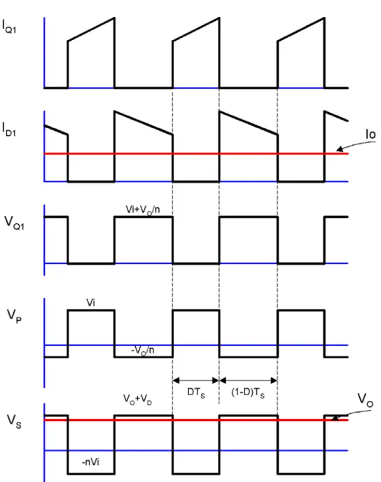
Figure 11. Flyback converter CCM waveforms
The simplified voltage conversion relationship for the flyback power stage operating in CCM is given by: D D n V V i O − × = 1
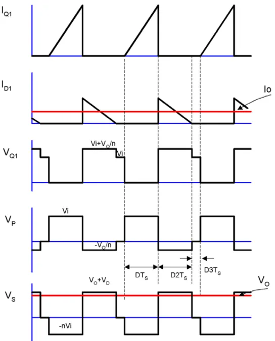
Figure 12. Flyback converter DCM waveforms
Flyback DC/DC Converter Small Signal Model (Transfer Function):
) 1 ) ( ( ) ( ) 1 ) ( ( ) ( ) 1 ( 1 ) ( ) ( T s Z s i T s GV s V T T H s V s V OUT load g g ref O = + + + − + ∧ ∧ ∧ ∧ gain loop V s GV s G s H s T( )= ( ) C( ) d( ) =
For CCM Mode:
*Two Pole fLC , One Zero fESR for GVd(s) and One Right-Half-Plane zero
z From a practical view, at RHP zero frequency, the loop gain starts increasing at a 20dB/decade rate but the loop phase decreases by –45 degrees (in a normal, LHP zero, the loop phase will increase by +45 degrees). This imposes the restriction that the gain be rolled off to 0dB before encountering the RHP zero.
z The output inductor, capacitor and the capacitor’s ESR must be selected so that the double pole occurs first and then the output capacitor zero and then the RHP zero. This assures that the loop gain crosses 0dB at a slope that is first order (20dB/decade) and that the instability inherently associated with the RHP zero is circumvented by crossing 0dB before the RHP zero frequency occurs.