HALF MODE SUBSTRATE INTEGRATED WAVEGUIDE BROADBAND BANDPASS FILTER
C.-L. Zhong, J. Xu, Z.-Y. Yu, M.-Y. Wang, and J.-H. Li
School of Physics and Electronics
University of Electronic Science and Technology of China Jianshe North Avenue, Chengdu, Sichuan 610054, China
Abstract—A planar half mode substrate integrated waveguide (HMSIW) broadband bandpass filter is proposed. It is realized by cascading a lowpass filter and a highpass filter. A transmission line with half mode substrate integrated waveguide (HMSIW) on the circuit board has the characteristic of highpass, while a periodic uniform photo band structure (PBG) array has the characteristic of bandstop. Combining these two structures, a novel compact broadband bandpass filter (BPF) is fabricated and measured. Measured results show that the proposed BPF has wide bandwidth from 11.8 GHz to 23.8 GHz, all the measured insert loss are less than 2.1 dB, return loss are less than 9 dB in the passband. The BPF achieves a wide stopband with 34 dB attenuation low to 5GHz and 27 dB attenuation up to 35GHz.
1. INTRODUCTION
coupling structure. This type of filter has low insertion loss, a small group delay variation within the central passband and relatively small size. But its stopband rejection at low frequency is low. In [5], Wang, Hong and colleagues designed the HMSIW bandpass filter using I-shaped slot coupling resonant structure, but the passband width of the filter is narrow. In [6], Naghshvarian-Jahromi and Tayarani designed a miniature planar UWB bandpass filters with circular slots in ground and in [7] Shobeyri and Vadjed Samiei designed a compact ultra-wide band bandpass filter with defected ground structure, but stopband rejection is low in all these UWB filters simulational results.
In this paper, we present a new method to design a bandpass filter with performances such as broadband passband (bandwidth of 67%), compact structure, higher rejection of out-band and no accessional passband. This filter is realized by cascading a lowpass filter and a highpass filter. A transmission line with half mode substrate integrated waveguide (HMSIW) structure on the circuit board has the characteristic of highpass [5], while a periodic uniform photo band structure (PBG) array structure forms stopband of high frequency [8, 9]. We realized lowpass by upper frequency’s stopband. Combining these two structures, a new broadband bandpass filter (BPF) is fabricated. Furthermore, the proposed filter has a relatively small size of 10 mm by 53 mm.
2. HMSIW FILTER ANALYSIS AND DESIGN
The proposed filter consists of a transmission line of HMSIW, a PBG array on HMSIW and a transition between microstrip and HMSIW as shown in Fig. 1. The three symmetrical I-shaped slots are etched on the circuit board. Each I-shaped slot is a PBG unit and three uniform I-slot-shaped PBG units form a PBG array. So this PBG array is periodic structure. We can analyze the characteristics of PBG structure’s frequency response using periodic structure theory as following.
Figure 1. Circuit of broadband bandpass filter.
Figure 2. Equivalent circuit of periodic circuit representing PBG structure.
at the center and using the well known transmission line formula [9]: Zin =Z0
Zl+jZ0tan(βul)
Z0+Zltan(βul)
(1) whereZo is the characteristic impedance andβu is the phase constant
(losses of the transmission line are assumed to be zero) of the transmission line,Zl is the loading impedance, andlis the line length.
The transmission line is approximated either by microstrip line or other transmission line depending on the width-height ratio of the line and the dielectric material.
The propagation constant (γ) for the infinite periodic structure is [12]:
cosh(γa) = cos(βua) +j
Z 2Z0
sin(βua) (2)
The characteristic impedance (Z0) and the phase constantγ, in Eq. (2)
attenuated, propagating wave on the periodic structure, and defines the pass-band of the structure. Eq. (3) reduces to
cos(βa) = cos(βua) +j
Z 2Z0
sin(βuα) (4)
which can be solved for β if the magnitude of the right hand side is less than or equal to unity. Condition β= 0, nπ/ain Eq. (3), gives
cosh(αa) = cos(βua) +j
Z Z0
sin(βuα) (5 )
which describes an attenuated wave alongxdirection, and this defines the stop-band of the structure.
According to above analysis, the HMSIW PBG array is basically a periodical structure that satisfies the following equation, and strongly shows band-stop filter characteristics as the number of cells is increased [8]:
k=π/L1 (6)
where k is the propagation constant. The cell distance (L1) is equal
to 1/2 guided wavelength (λg) ifkis equal to 2π/λg. The propagation
constant is difficult to determine and full-wave analysis is necessary to calculateλg for the structure in Fig. 1. As a simple approximation, it is
acceptable to set the propagation constant as approximately the same as an unperturbed transmission line, assuming that the perturbation of the PBG structure is very small [9–11]. The circuit length is dependent
on the cell number, center frequency, and dielectric constant. In this study, the substrate used is a RT/Duroid 5880, with relative dielectric constant (εr) of 2.2, height (H) of 0.254 mm, and length of 33 mm.
The stopband center or resonant frequency (fo) is chosen near 35GHz
and, thus, the distance of adjacent cells isL1 = 2.8 mm for aboutλg/2
and the number of cells is three. 3. EXPERIMENTAL RESULT
The dimensions of the microstrip transition sect are W1 = 0.76 mm
and W2 = 2.76 mm, and its length is L2 = 20 mm respectively. The
dimensions of the I-shaped PBG unit areA= 0.5mm andB = 3.1 mm. The distance between two adjacent PBG units is L1 = 2.8 mm, the
width of the HMSIW structure is W3 = 4 mm, and the length of the
HMSIW is L3 = 12.8 mm. The distance between the PBG unit and
the open circuit side of the HMSIW structure is W4 = 0.66 mm. The
numerical simulation was performed with electromagnetic simulator software — CST.
-40 -35 -30 -25 -20 -15 -10 -5 0 5
0 10 15 20 25 30 35 40
frequency (GHz) S-parameter (dB) measured S21 simulated S21 simulated S11 measured S11 5
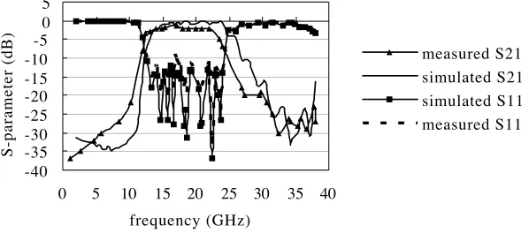
Figure 4. Measured (at normal temperature) and simulated S-parameters.
The simulated and measured results are shown in Fig. 4. Measured and simulated results agree approximately, except that the resonant frequency (fo) is shifted by ±1.4 GHz or ±7%. Measured inserted
loss about is 2.8 dB. This difference is mainly caused by nonsimulated effects of test fixture parasitic, copper thickness, and etching tolerance. It has been found that by changing the parameters of the I shaped PBG unit “A” and “B”, a different frequency resonator can be selected. In addition, by changing the distance “L1” of the two PBG unit, the
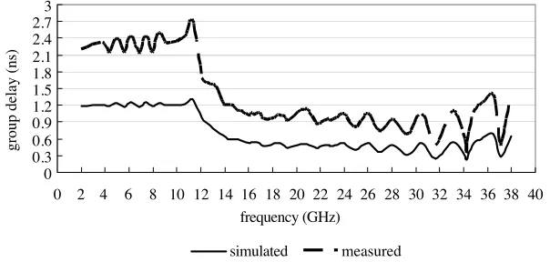
constant of 2.2. The filter was measured with an Agilent E8247C and an HP 8757D network analyzer (NA). The measured results are shown in Fig. 4, and S21’s group delay of this filter is as Fig. 5. The full
frequency passband is from 11.8 to 23.8 GHz, the bandwidth is about 67%. All the return loss are less than 9 dB, insert loss are less than 2.1 dB in the passband and it achieves a wide stopband with 18 dB attenuation up to 30 GHz in simulation. Respectively, the simulated results of the filter are also given in both figures for comparison.
0 0.3 0.6 0.9 1.2 1.5 1.8 2.1 2.4 2.7 3
0 10 12 14 16 18 20 22 24 26 28 30 32 34 36 38 40
frequency (GHz)
group delay (ns)
simulated measured
2 4 6 8
Figure 5. Measured and simulated S21 group delay (at normal temperature).
4. CONCLUSION
ACKNOWLEDGMENT
The authors would like to thank all members of millimeter wave research lab of the Physics and Electronic School for their helps in design and test of this filter.
REFERENCES
1. Kuo, J. T. and E. Shin, “Wideband bandpass filter design with three-line microstrip structures,” IEEE MTT-S Int. Microw. Symp. Dig., 1593–1596, May 2001.
2. Gao, J., L. Zhu, W. Menzel, and F. Bugelsack, “Short-circuited CPW multiple-mode resonator for ultra-wideband (UWB) bandpass filter,” IEEE Microw. Wirel. Compon. Lett., Vol. 16, 104–106, August 2006.
3. Wang, H., L. Zhu, and W. Menzel, “Ultra-wideband bandpass filter with hybrid microstrip CPW structure,” IEEE Microw. Wirel. Compon. Lett., Vol. 15, 844–846, December 2005,
4. Yang, G. M., R. H. Jin, and J. P. Geng, “Planar microstrip UWB bandpass filter using U-shaped slot coupling structure,”
Electronics Letters, Vol. 42, No. 25, December 2006.
5. Wang, Y., W. Hong, and Y. Dong, “Half mode substrate integrated waveguide (HMSIW) bandpass filter,” IEEE Microw. Wirel. Compon. Lett., Vol. 17, 265–267, April 2007.
6. Naghshvarian-Jahromi, M. and M. Tayarani, “Miniature planar UWB bandpass filters with circular slots in ground,” Progress In Electromagnetics Research Letters, Vol. 3, 87–93, 2008.
7. Shobeyri, M. and M. H. Vadjed Samiei, “Compact ultra-wide band bandpass filter with defected ground structure,” Progress In Electromagnetics Research Letters, Vol. 4, 25–31, 2008.
8. Ahn, D., J. Park, C. Kim, J. Kim, Y. Qian, and T. Itoh, “A design of the low-pass filter using the novel microstrip defected ground structure,” IEEE Trans. Microw. Theory Tech., Vol. 49, 86–92, January 2001.
9. Rahman, M. and M. A. Stuchly, “Modeling and application of 2D photonic band gap structures,” IEEE Proceedings ofAerospace Conference,Vol. 2, 893–898, March 2001.
10. Yun, T. Y. and K. Chang, “Uniplanar one-dimensional photonic-bandgap structures and resonators,” IEEE Trans. Microwave Theory Tech., Vol. 49, 549–553, March 2001.