Available online:
http://edupediapublications.org/journals/index.php/IJR/
P a g e | 6 4 3Low Power Testable Reversible Sequential Circuits implementation on FPGA
P. Rahul Reddy
11
Associate Professor, Department of ECE, Arjun College of Technology and Science, RangaReddy,Telangana, India
Abstract
In this paper suggested reversible sequential circuits based on conservative logic that's checkable for any unidirectional stuck-at faults using only 2 test vectors, that consists of all 0s and all 1s. So our novel proposed sequential circuits basically depends on particular conservative logic gates that role is to exceed the sequential circuit as previously realized in classical gates in the case of testability. As mentioned the considered sequential circuit’s implemented by employing typical classic gates don't offer heritable support for testability. Hence, a standard sequential circuit desires modification within the unique circuitry, its role is to offer the testing capability. We have a tendency to for presenting a brand new conservative gate referred to as multiplexer conservative QCA gate (MX-cqca) that's not reversible in nature nevertheless has analogous properties because the Fredkin gate seem to be operating as 2:1 multiplexer. At last our proposed MX-cqca gate surpasses the Fredkin gate as far as many-sided quality (the quantity of larger majority voters), speed, and area.
Key Words: Conservative Logic, Fredkin Gate, Quantum-Dot, Reversible Logic.
--1. INTRODUCTION
Among the rising computing paradigms, reversible logic seems to be promising as a result of its wide applications in rising technologies and large number of the rising nanotechnologies that have numerous applications in case of reversible logic which are like quantum dot cellular
automata, quantum computing, optical computing,
Spintronics, deoxyribonucleic acid computing, molecular
computing and additionally in power-efficient
nanocomputing, etc. Reversible circuits are those circuits that don't lose data during computation and reversible computations during a system are often performed only if the system includes of reversible gates. These circuits will generate distinctive output vector from every input of the vector, and the other way around, that is, there's a one-to-one mapping between the input and also the output vectors. As a elementary contribution in [2], Landauer has shown that in irreversible computation one little bit of data lost leads to KTln2 Joules of energy dissipation flier in another
seminal contribution [3], proved that this KTln2 joules of
energy dissipation won't occur if computation is performed in an exceedingly reversible manner an N × N (N inputs and N outputs) reversible gate are often represented as
Iv = I1, I2, I3, I4………... IN (1)
Ov = O1, O2, O3, O4………. ON (2)
where Iv and Ov signify input and output vectors,
respectively.
1.1 Rev ers ib le lo g ic g ates :
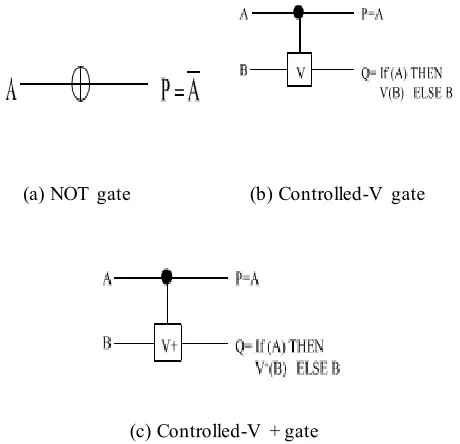
Any reversible gate is complete exploitation the 1x1 NOT gate, and 2x2 reversible gates like Controlled-V and Controlled-V + (V could be a square-root-of NOT gate and
V + is its Hermitian) and therefore the Feynman gate that is additionally called the Controlled NOT gate (CNOT). Thus, in easy terms, the quantum price of a reversible gate is calculated by counting the numbers of NOT, Controlled-V,
Controlled-V+ and CNOT gates needed in its
implementation.
The NOT Gate: A NOT gate could be a 1x1 gate depicted as shown in Fig. 1.1(a). Since it's a 1x1 gate, its quantum price is unity. The controlled-V gate is shown in Fig. 1.1(b) within the controlled-V gate, once the control signal A=0 then the qubit B can meet up with the controlled half unchanged, i.e., we'll have Q=B. once A=1 then the unitary operation V = i+1/2 is applied to the input B, i.e., Q=V (B). The controlled-V+ gate are shown in Fig. 1.1(c) within the
management controlled-V+ gate once the control signal A=0 then the qubit B can go through the controlled part unchanged, i.e., we'll have Q=B. once A=1 then unitary operation V+ = V−1 is applied to the input B, i.e., Q=V+(B).
The V and V+ quantum gates have the subsequent
properties:
V × V = NOT V × V+ = V + × V = I
V+ × V+ = NOT
Available online:
http://edupediapublications.org/journals/index.php/IJR/
P a g e | 6 4 4V+ gates in series additionally perform as a NOT gate. A V gate in series with V+ gate, and contrariwise, is an identity.
(a) NOT gate (b) Controlled-V gate
(c) Controlled-V + gate
Fig. 1.1. NOT, Controlled-V and Controlled-V+ gates
Th e Fey n man Gate (CNOT Gate)
The Feynman gate (FG) or the Controlled-NOT gate (CNOT) may be a pair of inputs a pair of outputs reversible
gate having the mapping (A, B) to (P=A, Q=A⊕B)
wherever A, B are the inputs and P, q are the outputs, respectively. Since it's a 2x2 gate, it's a quantum cost of 1. Fig's 2.1(a) and 2.1(b) demonstrate the piece outlines and quantum representation of the Feynman gate. The Feynman gate is utilized for replicating the sign in this way evading the fan-out issue in reversible rationale as appeared in Fig.2.1(c). Further, it is even be utilized for producing the complement of a signal as appeared in Fig.2.1 (d).
(a) An CNOT gate (b) An Quant u m rep res en tatio n CNOT g ate
(c) Feynman gate for avoiding the fanout (d) Feynman gate for generating the complement of a signal
Fig. 2.1. CNOT gate, its quantum implementation and its useful properties
Th e To ffo li Gate
Here as mentioned Toffoli Gat (TG) is a 3x3 two-through reversible gate as appeared in Fig. 3.1(a). Two through means two of its yields are the same as the inputs with that of the mapping (A, B, C) to (P=A, Q=B, R=A·B⊕ C), whereas A, B, C are inputs and P, Q, R are yields, individually. Therefore Toffoli gate is a popular amongst the most well-known reversible entryways and has the quantum expense of 5 as appeared in Fig. 3.1(b) [4]. The quantum expense of Toffoli entryway is 5 as it needs 2V gate, 1 V+ gate and 2 CNOT gate to execute
(a) Toffoli gate (b) Quantum imp lementatio n o f To ffo li Gate
(c) Graphical notation of Toffoli gate
Fig.3.1. Toffoli gate and its quantum implementation
1.2
Bas ics of QCA Comp ut ingAvailable online:
http://edupediapublications.org/journals/index.php/IJR/
P a g e | 6 4 5cell has two additional electrons that possess the diagonals inside of the cell because of electrostatic shock.
(a) QCA 4 dots (b) QCA cell as logic ’1’ and logic ’0’
At the point when electrons are in dots 1 and 3, P = - 1 (Logic '0') and when electrons in dots 2 and 4, P = +1 (Logic '1'). Figures 6.1(a) and 6.1(b) demonstrate the 4 quantum dots in a QCA cell, and the execution of Logic "0" and Logic "1" in a QCA cell.
P = (P2 + P4) − (P1 + P3)/P1 + P2 + P3 + P4… ….. ( 3)
The fundamental QCA device is the treated as majority voter or else as majority gate, and produces output function as F=AB+BC+AC, where F is treated as majority of the inputs A, B and C. The dominant part voter can be made to act as an AND gate or as an OR gate, by setting one of the inputs as "0" and '1', individually as appeared in fig 6.1(c).Another essential gate in QCA is the inverter, which is shaped when a QCA cell, say cell-1 is set 45 degrees to another QCA cell, for instance cell-0, cell-1 gets the backwards estimation of cell-0. There can be numerous methods for outlining the QCA inverter, one of which is appeared in Fig.6.
(c) Majority voter (d) Inverter
From above discussions in QCA computing, the signal transfer is prepared through wires which are broadly of two types (i) Binary wire, (ii) Inverter chain.
(e) Binary wire f) Inverter chain
Fig. 6.1 QCA Computing
The electrons in adjacent QCA cells act with one another leading to propagation of the polarization from one cell to a different. Therefore, a QCA wire is shaped by prearrangement the QCA cells in the course of a series during which all the neighboring cells can get the polarization of the driver cell (input). The binary wire is shown in Fig. 6.1(e).
Each cell during this arrangement has opposite polarization of their neighbors as they act reciprocally. The inverter chain is shown in Fig. 6.1(f). In QCA, once a binary wire crosses the inverter chain, there's no interaction between the two; thus the signals within the electrical converter chain and binary wire will jump over one another.
2.0 PROPOSED SYSTEM
For numerous of the designs, the designer might in theory be attentive in exploitation the testing advantages of conservative logic however convertible the quantity of QCA cells. Thus, during this work we tend to propose a replacement conservative logic gate that's conservative in nature however isn't reversible.
.
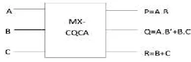
Fig.7 proposed MX-CQCA gate
The proposed traditionalist gate is named multiplexer Conservative QCA gate (MX-CQCA) that has three inputs as well as three outputs. Henceforth the MX-CQCA has one amid where its yields working as a multiplexer which will facilitate in mapping the sequential circuits supported it, whereas the opposite 2 outputs work as AND as well as OR gates only. So here the mapping of the particular inputs to
outputs of the MX-CQCA is: P= AB; Q=AB‟ +BC;
Available online:
http://edupediapublications.org/journals/index.php/IJR/
P a g e | 6 4 6the outputs, respectively. Fig.7 shows the diagram of the MX-CQCA gate. Table 1 shows the exact truth table of our proposed MX-CQCA gate.
Tab le 1 Tru th Tab le o f M X-CQCA g ate
Th e table verifies the gate’s conservative logic natu re, i.e., th at the numbers of 1s in the inputs is equal to the number of 1s in th e o u tp u ts .
Fig.8QCA model of MX-CQCA
From Fig. 8, we will see that the proposed MX-CQCA gate needs four clocking zones and 5 majority gates for its QCA implementation the essential component of QCA circuits is majority gate and invertors. Hence, expeditiously constructing QCA circuit’s exploitation majority gates has attracted plenty of attention [9]. QCA computing is one the promising technology that job is to implement basic reversible logic gates. So treated QCA design of Fredkin gate has four-phase clocking scheme, during which the clocking zone is denoted by the quantity next to D (D0 means that clock zero zone, D1 means that clock one zone and then on). The Fredkin gate has 2 level majority voters (MV) implementation, and it needs six MVs and four clocking zones for implementation. The quantity of clocking zones during a QCA circuit represents the delay of the circuit [1] (delay between the inputs and therefore the
outputs). Higher the numbers of clocking zones lower the operative speed of considered circuit.
2.1 Design Methodology for Nonreversible Testable Design Bas ed On M x-Cq ca Gate
The proposed conservative gate MX-CQCA is helpful to design any majority logic and multiplexer logic-based testable nonreversible circuits within the existing literature, thirteen customary functions are proposed to represent all three-variable Boolean functions [8]. These 13 functions are wide utilized in QCA and majority logic-based synthesis. So as to design any complex function based on MX-CQCA, the proposed design methodology is summarized within the following 3 steps.
1) Stag e 1: The input function is disintegrated into the Boolean system amid which every node has about 3 variables. This stride is similar to the outline approach proposed.
2) Stag e 2: The 3 variable work produced at every node in Step one is mapped to its MX-CQCA-based usage. The mapping relies on the library of thirteen customary functions enforced exploitation the MX-CQCA.
3) Step 3: The nodes that have fan-out of quite one are known, and MX-CQCA gates are used to form the copy of the signals, that have fan-out of over one.
3.0 . IM PLEM ENTA TION A ND RESULTS
Researchers have worked on numerous phases of reversible logic testing, like fault modeling, test pattern generation and several supplementary areas. This section deliberates variety of dissimilar methodologies to come up with on-line testable reversible circuits declared within the collected works and discovers the considerations regarding their designs on error detection.
Available online:
http://edupediapublications.org/journals/index.php/IJR/
P a g e | 6 4 7Fig.10. RTL Schematic of Fredkin gate.
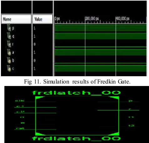
Fig 11. Simulation results of Fredkin Gate.
Fig 12. Design of testable reversible D latch.
Fig15. Fredkin gate-based testable reversible masterslave D flip-flop
4.0 CONCLUSIONS
In this paper, we have a tendency to propose the design of 2 vectors testable sequential circuits supported conservative logic gates. As talked about before our proposed consecutive circuits established on conventional logic gates surpass the successive circuits executed in traditional gates as far as testability. The reversible outline of the DET flip-flop is proposed for the essential time inside of the writing. We tend to moreover demonstrate the utilization of the proposed approach toward 100% shortcoming scope for single
missing/extra cell flaw inside of the quantum dot cell automata (QCA) layout of the Fredkin gate.
REFERENCES
[1] Dalui M, Sen B, and Sikdar B. K, (2010) „Fault tolerant QCA logic design with coupled majority-minority gate, ‟ Int. J. Comput. Appl., vol. 1, no. 29, pp. 81–87.
[2] R. Landauer. Irreversibility and heat generation in the computational process. IBM J. Research and Development, 5:183– 191, December 1961.
[3] C.H. Bennett. Logical reversibility of computation. IBM J. Research and Development, 17:525–532, November 1973.
[4] H. Thapliyal and N. Ranganathan, ‘‘Reversible logic-based concurrently testable latches for molecular QCA,’’ IEEE Trans. Nanotechnol., vol. 9, no. 1, pp. 62--69, Jan. 2010.
[5] P. Tougaw and C. Lent, ‘‘Dynamic behavior of quantum cellular automata,’’ J. Appl. Phys., vol. 80, no. 8, pp. 4722--4736, Oct. 1996.
[6] M. B. Tahoori, J. Huang, M. Momenzadeh, and F. Lombardi, ‘‘Testing of quantum cellular automata,’’ IEEE Trans. Nanotechnology., vol. 3, no. 4, pp. 432--442, Dec. 2004.
[7] G. Swaminathan, J. Aylor, and B. Johnson, ‘‘Concurrent testing of VLSI circuits using conservative logic,’’ in Proc. Int. Conf. Comput. Design, Cambridge, MA, Sep. 1990, pp. 60--65.
[8] S. F. Murphy, M. Ottavi, M. Frank, and E. De Benedictis, 2006 “On the design of reversible QDCA systems,” Sandia National Laboratories, Albuquerque, NM, Tech. Rep. SAND2006-5990.
[9] Ravi1 T and Kannan V,„A Novel Design of D-Flip Flop Using New RR Fault Tolerant Reversible Logic Gate‟.