238 |
P a g e
ANALYSIS AND DESIGN OF HIGH BOOST RATIO
CONVERTER FOR EFFICIENT ENERGY TRANSFER
FROM PV MODULE
Nithin N.V
1, Someswari T
21
Dept. of EEE , The Oxford College of Engineering , Bengaluru , (India )
2
Dept. of EEE , The Oxford College of Engineering , Bengaluru , (India )
ABSTRACT
Attempts were made by scientists for utilizing solar power in different ways. Solar drives, solar water heater, solar
concentrators are some examples. Recently because of energy shortage attention was given for generating electric
power from solar power. This proposed project presents a non-isolated, high boost ratio hybrid transformer dc-dc
converter that has the applications in low voltage renewable energy sources. The proposed converter makes use of a
hybrid transformer to transfer the inductive and capacitive energy simultaneously. This helps to achieve a high
boost ratio .The proposed system combines pulse width modulation along with resonant mode operation. This helps
to minimize the turn off losses of the switch and thereby improving the efficiency of the converter. Since the input to
the converter is hybrid linear sinusoidal current waveform, the input current ripple and conduction losses are low.
The voltage stresses on the active switch and diodes are maintained at a low level and are independent of the
changing input voltage over a wide range as a result of the resonant capacitor transferring energy to the output of
the converter.
Keywords
:Energy Sources with Low Dc Voltage, High Boost Ratio Dc–Dc, High Efficiency, Hybrid
Transformer, Photovoltaic (Pv) Module.
I. INTRODUCTION
As the non-renewable energy is getting exhausted and its cost being high , the demand for renewable energy is
increasing and non-renewable energy sources like PV modules have been widely used . Power conditioning systems
(PCS) is used for integrating the power from the PV module into the existing power distribution system. PCS can be
single-stage or a double-stage [1]–[7], [15], [16]. In double-stage PCS dc–dc conversion stage is connected to either
a low-power individual inverter or a high-power centralized inverter that multiple converters could connect to. The
dc–dc conversion stage of the PCS requires a high efficiency, high boost ratio dc– dc converter to increase the low
dc input voltage from the PV panel to a higher dc voltage.
239 |
P a g e
efficient and more expensive due to the increased manufacturing costs. For a two stage PCS , a non-isolated dc–dcconverter with high boost ratio is more suitable because it can be easily integrated with current PV systems and the
cost can also be reduced and provides higher efficiency [1]. The output voltage range from a PV panel varies and so
it would be better to use a system with the high efficiency so that maximum output can be obtained during different
operating conditions. Dc–dc converter in PV applications is also used to implement maximum power point tracking
(MPPT). A large cluster of PV could maintain maximum power output from each panel without interfering with the
other panels in the system if it is possible to implement MPPT for each individual PV panel. The major
consideration to implement an accurate MPPT is that the input current ripple of the converter has to be low.
For PV module converter applications, the high efficiency over a wide load range and input voltage range is
extremely important because the performance is weighted differently for specific load levels and input voltages. In
this paper, a high boost ratio dc–dc converter with hybrid transformer is presented in order to achieve high
efficiencyover wide input voltage and output power ranges. A small resonant inductor is added and the capacitance
of the switched-capacitor in the energy transfer path is reduced and this modification helps to achieve a hybrid
operation mode [17], [18], which combines pulse width modulation (PWM) and resonant power conversions. This
method is introduced in the proposed high boost ratio dc–dc converter.
The total power delivered is increased by transferring the inductive and capacitive energy simultaneously and
thereby the losses in the circuit are also decreased. The two transformer modes, where the transformer operates
under normal conditions and where it operates as a coupled-inductor, are combined together and therefore the
magnetic core can be used more effectively and smaller magnetics can be used. Smaller current ripple than the
previous high boost ratio converter topologies is achieved by the continuous input current of the converter. Since the
current ripple is low, the input capacitance can be reduced and it is easier to implement a more accurate MPPT for
PV modules. The conduction losses in the transformer are greatly reduced because of the reduced input current RMS
value through the primary side. The voltage stress of the active switch is independent of the input voltages. The
turn-off current of the active switch is reduced due to the introduction of the resonant portion of the current. The
decreased RMS current value and smaller turn-off current of the active switch helps to enhance high efficiency at
light output power level and low-input voltage operation. The voltage stresses of the diodes are kept under the
output dc bus voltage.
II. PROPOSED CONVERTER TOPOLOGY ANDOPERATION ANALYSIS
Fig. 1 shows the circuit diagram of the proposed high boost ratio hybrid dc-dc converter with various components.
Cin is the input capacitor; HT is the hybrid transformer having the turns ratio 1:n; S1 is the active MOSFET switch;
D1 is the clamping diode, that provides a current path for the leakage inductance of the hybrid transformer when S1
is OFF, Cc captures the leakage energy from the hybrid transformer and transfers it to the resonant capacitor Cr by
means of a resonant circuit composed of Cc , Cr , Lr , and Dr ; Lr is a resonant inductor, which operates in the
240 |
P a g e
portion of the circuit. Cr is a resonant capacitor, which operates in the hybrid mode. The turn-on of Dr is determinedby the state of the active switch S1. D0 is the output diode and Co is the output capacitor. Ro is the equivalent
resistive load at the output side.
Fig. 1.Proposed High Boost Ratio Dc–Dc Converter With Hybrid Transformer
Fig. 2 illustrates the five steady-state topology stages of the proposed dc–dc converter for one switching cycle. Fig. 3
shows the key voltage and current waveforms for specific components of the converter over the switching cycle. In
Fig. 3, g1 represents the driver signal for the active MOSFET switch S1 ; is1 is the current of the MOSFET S1 ; iCr is
the current of the resonant capacitor Ct ; iCc is the current of clamping capacitor Cc ; iin is the primary side current of
hybrid transformer; io is the current through the output diode; vs1 and vDo are the voltage waveforms of the active
switch MOSFET S1 and the output diode D0 , respectively.
The five operation modes are briefly described as follows.
[t0 ,t1 ], [Fig. 2(a)]: In this period, MOSFET S1 is ON, the magnetizing inductor of the hybrid transformer is charged
by input voltage, Cr is charged by Cc , and the secondary-reflected input voltage nVin of the hybrid transformer
together by the resonant circuit composed of secondary side of the hybrid trans-former, Cr , Cc , Lr , and Dr . The
energy captured by Cc is transferred to Cr , which in turn is transferred to the load during the off-time of the
MOSFET. The current in MOSFET S1 is the sum of the resonant current and linear magnetizing inductor current.
The main advantage of linear and resonant hybrid mode operation is that the energy is delivered from source during
the capacitive mode and inductive mode simultaneously. The turn-off current is also decreased, which causes a
reduction in the turn-off switching losses.
[t1 ,t2 ], [see Fig. 2(b)]: At time t1 , MOSFET S1 is turned OFF, the clamping diode D1 is turned ON by the leakage
energy stored in the hybrid transformer during the time period that the MOSFET is ON and the capacitor Cc is
charged which causes the voltage on the MOSFET to be clamped.
[t2 ,t3 ], [see Fig. 2(c)]: At time t2 , the capacitor Cc is charged to the point that the output diode Do is forward
biased. The energy stored in the magnetizing inductor and capacitor Cr is being transferred to the load and the clamp
diode D1 continues to conduct while Cc remains charged.
[t3 ,t4 ], [see Fig. 2(d)]: At time t3 , diode D1 is reversed biased and as a result, the energy stored in magnetizing
steady-241 |
P a g e
state operation, the charge through capacitor Cr must satisfy charge balance. The key waveform of the capacitor Crcurrent shows that the capacitor operates at a hybrid-switching mode, i.e., charged in resonant style and discharged
in linear style.
[t4 ,t0 ], [see Fig. 2(e)]: The MOSFET S1 is turned ON at time t4 . Due to the leakage effect of the hybrid transformer,
the output diode current io will continue to flow for a short time and the output diode Do will be reversed biased at
time t0 ; then the next switching cycle starts.
Fig.2.Operation modes of the high boost ratio converter with hybrid transformer. (a) t0 -t1.(b) t1 -t2.(c) t2 -t3. (d) t3 -t4.(e) t4 -t5
The boost ratio Mb is obtained by three flux balance criteria for the steady state. The first flux balance on the
magnetizing inductor of hybrid transformer indicates that in steady state :
VCc= Vin (1)
1-D
Second, according to flux balance on the resonant inductor during on time
.V
Cr=nV
in+ V
Cc= (n + 1 ) V
in(2)
1-D
The last flux balance that governs the circuit is voltage-second balance of the magnetizing inductor in the hybrid
242 |
P a g e
V
inD = V
o– V
Cr– V
in(1-D)
(3)
1+n
By substituting (2) into (3), the boost conversion ratio can be obtained
Mb =
V
o= n+2
(4)
V
in1-D
III SIMULATION DIAGRAM AND RESULTS
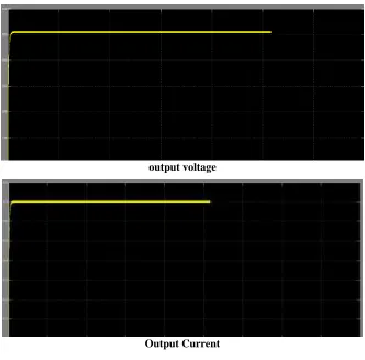
Fig 4: Simulation Model of Open Loop Circuit of High Boost Ratio Dc-Dc Converter
243 |
P a g e
output voltageOutput Current
Fig 4: Simulation Results
IV. EXPERIMENTAL VERIFICATIONS
A prototype circuit that can be used for PV module power optimizer applications was built and tested to verify the
effectiveness of the proposed converter. Tables given below list the design parameters and components selection for
the converter. Two control methods can be adopted for the proposed converter. The first method is the variable
frequency control, which is done by using a fixed Ton and varying the Toff to obtain the desired gain. Another control
method is the PWM converter control by adjusting the duty cycle of the switch. In real control implementation,
PWM control with fixed switching frequency is preferred because of its simplicity.
Table I Design Parameters
Rated Power 220 W
DC Bus Voltage 500 Vdc
Input Voltage Range 20V-45V
Output Power Range 30W-220W
Switching Frequency 74.5 kHz
Turns Ratio n of Hybrid
244 |
P a g e
Table IIComponents Selection
Cin 5*10µF/100V ceramic caps
Hybrid Transformer ETD 34 with Lm = 18µH
S1 BSC077N12NS3
Cr 1µF/600V Film Cap
D1 V12P12-M3
Lr 2.2µH
Cc 2*10µF/100V ceramic caps
Dr, Do HFA15TB60S
C0 2µF/600V Film Cap
The prototype of the proposed converter was designed to convert the low dc voltage, Vin with the voltage ranging
from 20 to 45 V, to a constant high dc output, Vo = 500 V. To maintain a low voltage stress on the active switch M1
and reasonable duty cycle range, the turns ratio n of hybrid transformer was chosen to be 40:9. The resonant
contribution index kr = 0.35 was when D = 0.5. The duty ratio range for an input PV module voltage range of 20–45
V is 0.28–0.68, which is kept within a reasonable range.
V. ADVANTAGES OVER CONVENTIONAL NON-RESONANT HIGH STEP-UP CONVERTER
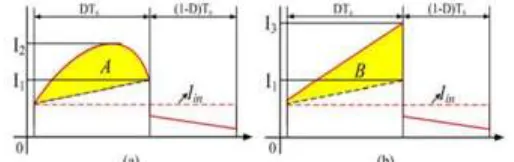
Fig. 5. Input Current Comparison Between Resonant Mode And Linear Mode: (A) Resonant Mode. (B) Linear Mode.
The methods in existence that are used to achieve high boost ratio for non-isolated dc–dc converters involves the
usage of coupled-inductor and switched-capacitor techniques [8]–[14]. The converter presented in this paper makes
use of hybrid-switching technique [17], [18] that combines PWM and resonant power conversion method to achieve
a high boost ratio while maintaining a high efficiency. There are many advantages gained by the usage of the
hybrid-switching operation.
The input currents for the resonant sinusoidal charge mode and the PWM linear charge mode are shown in Fig. 5.
The converter that is proposed in this paper works on the basis of resonant sinusoidal charge mode, while a
conventional non-resonant con-verter [11] works using the linear charge mode. If the output power is fixed and
245 |
P a g e
and B (see Fig 5) show the capacitive energy transferred bythe hybrid transformer of the proposed converter withresonant mode and linear energy transferred by the coupled-inductor of conventional non-resonant converter. The
switching losses for a dc–dc converter are directly proportional to the switching current given by the fixed
conversion voltages. As mentioned above in circuit operation, the MOSFET is turned ON at time t = t4 , the fast rate
of change of the primary current is limited by the leakage inductor of the hybrid transformer thus reducing the
turn-on losses. Now the main switching loss is the turn-off switching losses.
The turn-off switching current I1 , as shown in 5(a)consists of only the magnetizing current because of the resonant
operation. For the conventional non-resonant converter [11], the turn-off switching current I3 , as shown in Fig. 5(b),
is the sum of the magnetizing current and the switched-capacitor charge current, which is dependent on the leakage
inductance of the coupled-inductor. For a given capacitor value of the, An increase in the leakage inductance can
reduce the raising rate of the primary side current in order to reduce the turn-off current, for a fixed
switched-capacitor value. However, the conversion ratio will decrease because of the reduced coupling factor k of the
coupled-inductor [11]. Because of this, the leakage inductance design of the coupled-inductor has a tradeoff between
the conversion ratio and a higher turn-off switching current.
The primary peak current I2 , as shown in Fig. 5(b), is smaller than the peak current I3of its switched-capacitor
because of the introduction of a resonant operation mode into the PWM converter for the proposed converter. The
capacitance of the charge capacitor Cr can be greatly reduced since the resonant modeis employed as opposed to the
switched-capacitor mode. The advantage of using the resonant mode is that it allows the use of smaller sized
magnetic components and lower profile charge capacitors for Cr. This can be used in application where a low profile
PV-module-integrated dc– dc converter is needed. The leakage inductance of the hybrid transformer can also be
effectively utilized as part of the resonant minor loop.
VI. CONCLUSION
In this paper a high boost ratio dc–dc converter with hybrid transformer that is suitable for renewable energy sources
with low dc voltage input is proposed. In this, we are implementing resonant conversion mode along with pulse
width modulation technique with coupled-inductor and switched-capacitor and we obtain the following features and
benefits:
1)The converter has an advantage that it transfers the capacitive and inductive energy simultaneously and this
enables to achieve higher efficiency by increasing the total power delivery by reducing losses in the system.
2)The conduction loss in the transformer and MOSFET is reduced because of the low-input RMS current and the
switching loss is also reduced because of the lower turn-off current. The converter can maintain high efficiency
under low-input voltage conditions because of these modifications.
3)The converter is suitable for PV module and fuel cell PCS because of the low-input ripple current feature and it
helps to enhance accurate MPPT by the dc–dc converter.
A prototype-circuit that can be used for PV module applications was made and tested with 20–45 V input voltage
246 |
P a g e
output diode voltage was under 350 V. These results were independent of the input voltage level.REFERENCES
[1] J.-S. Lai, ―Power conditioning circuit topologies,‖ IEEE Ind. Electron.Mag., vol. 3, no. 2, pp. 24–34, Jun.
2009.
[2] S. B. Kjaer, J. K. Pedersen, and F. Blaabjerg, ―A review of single-phase grid-connected inverters for
photovoltaic modules,‖ IEEE Trans. Ind.Appl., vol. 41, no. 5, pp. 1292–1306, Sep./Oct. 2005.
[3] F. Blaabjerg, Z. Chen, and S. B. Kjaer, ―Power electronics as efficient interface in dispersed power
generation systems,‖ IEEE Trans. PowerElectron., vol. 19, no. 5, pp. 1184–1194, Sep. 2004.
[4] Y. Xue, L. Chang, S. B. Kjaer, J. Bordonau, and T. Shimizu, ―Topolo-gies of single-phase inverter for small
distributed power generators: An overview,‖ IEEE Trans. Power Electron., vol. 19, no. 5, pp. 1305–1314,
Sep. 2004.
[5] B. Liu and S. Duan, ―Photovoltaic DC-building-module-based BIPV system-concept and design
considerations,‖ IEEE Trans. Power Elec-tron., vol. 26, no. 5, pp. 1418–1429, May 2011.
[6] Q. Li and P. Wolfs, ―A review of the single phase photovoltaic module in-tegrated converter topologies with
three different DC link configurations,‖ IEEE Trans. Ind. Electron., vol. 23, no. 23, pp. 1320–1333, Apr.
2008.
[7] W. H. Li and X. N. He, ―Review of non-isolated high step-up DC/DC converters in photovoltaic
grid-connected applications,‖ IEEE Trans. Ind.Electron., vol. 58, no. 4, pp. 1239–1250, Apr. 2011.
[8] Q. Zhao and F. C. Lee, ―High-efficiency, high step-up dc–dc converters,‖ IEEE Trans. Power Electron., vol.
18, no. 1, pp. 65–73, Jan. 2003.
[9] K. C. Tseng and T. J. Liang, ―Novel high-efficiency step-up converter,‖Proc. Inst. Elect. Eng.—Elect. Power
Appl., vol. 151, no. 2, pp. 182–190,Mar. 2004.
[10] T. J. Liang and K. C. Tseng, ―Analysis of integrated boost-flyback step-up converter,‖ Proc. Inst. Elect.
Eng.—Electr. Power Appl., vol. 152, no. 2, pp. 217–225, Mar. 2005.
[11] R. J. Wai and R. Y. Duan, ―High step-up converter with coupled-inductor,‖ IEEE Trans. Power Electron.,
vol. 20, no. 5, pp. 1025–1035, Sep. 2005.
[12] 21W. S. Yu, C. Hutchens, J.-S. Lai, J. Zhang, G. Lisi, A. Djabbari, G. Smith, and T. Hegarty, ―High
efficiency converter with charge pump and coupled inductor for wide input Photovoltaic AC module
applica-tions,‖ in Proc. IEEE Energy Convers. Congr. Expo., 2009, pp. 3895– 3900.
[13] 22S. M. Chen, T. J. Liang, L. S. Yang, and J. F. Chen, ―A cascaded high step-up dc–dc converter with single
switch for microsource application,‖ IEEE Trans. Ind. Electron., vol. 26, no. 4, pp. 1146–1153, Apr. 2011.
[14] 23T. F. Wu, Y. S. Lai, J. C. Huang, and Y. M. Chen, ―Boost converter with coupled inductors and buck–
boost type of active clamp,‖ IEEE Trans.Ind. Electron., vol. 55, no. 1, pp. 154–161, Jan. 2008.
[15] R. J. Wai, C. Y. Lin, R. Y. Duan, and Y. R. Chang, ―High-efficiency power conversion system for
247 |
P a g e
3702–3714, Oct. 2008.[16] 30W. Yu, J. S. Lai, H. Qian, and C. Hutchens, ―High-efficiency MOSFET inverter with H6-type
configuration for photovoltaic non-isolated AC-module applications,‖ IEEE Trans. Power Electron., vol. 56,
no. 4, pp. 1253–1260, Apr. 2011.
[17] 26S. Cuk and Z. Zhang, ―Voltage step-up switching dc-to-dc converter field of the invention,‖ U.S. Patent 7
778 046, Aug. 2010.
[18] 27S. Cuk, ―Step-down converter having a resonant inductor, a resonant capacitor and a hybrid transformer,‖