Waveguide Coupled Microstrip Patch Antenna a New Approach
for Broad Band Antenna
Sahana K* and Nandakumar M. Shetti
Abstract—A new technique is developed to couple the advantages of both the microstrip patch antenna and rectangular waveguide. An equilateral triangle is used as a radiating patch. This patch is fabricated on one face of a single-layer dielectric substrate with double-sided copper clad coated with tin, and on the other face an iris is fabricated and coupled to the waveguide. Antenna parameters such as return loss and bandwidth are studied for a circular patch. The results obtained are discussed in detail and explained. Matlab PDE toolbox is used to generate two-dimensional meshes. These meshes are converted into a three-dimensional form using subdomain numbers. RWG basis functions are used for MoM to calculate impedances. Reflection coefficient and 2D current are obtained using the complex impedances.
1. INTRODUCTION
The rapid advancement in the wireless communication led to the development of more efficient antennas. Microstrip patch antennas are increasing in popularity for the use in wireless applications. However, the main disadvantage of microstrip antennas is the narrow bandwidth and low gain. Different feeding techniques are used to overcome the problem of narrow bandwidth. In this study, waveguide coupling technique is used for improving the bandwidth. Waveguide Coupled Microstrip Patch Antenna (WCMPA) [1] consists of two patches, one radiating patch which faces open air, and the other faces the open end of the rectangular waveguide. WCMPA incorporates attractive features of microstrip antenna such as low prole, light weight, compact size and conformable structure, and easy fabrication, and it also possesses good features of waveguide, such as high power handling capability and low losses (resistive) [8]. In this technique, microstrip antenna is directly mounted on the mouth of the waveguide. Thus, maximum energy is radiated. The patch on the mouth of the waveguide which is of rectangular ring shape acts as a matching load to absorb maximum energy.
In this study, the microstrip is made up of double-sided glass epoxy printed circuits board. The size of the patch is such that it fits perfectly on the face of the waveguide matching all the four holes. It has two patches, one on the radiating side and the other on the waveguide side. The literature reveals a rectangular slot which resembles an iris type radiator proposed by Slatter [2], so for further study this pattern is retained, and the systematic study is performed on this type of waveguide coupled microstrip patch antenna. In this paper, a circular patch is used as a radiating element.
2. CONSTRUCTION
The proposed antenna is fabricated on an FR-4 epoxy laminate with a dielectric constant = 4.4 and thicknessh= 1.6 mm. The radiusr of the circular radiating patch is given by Balanis [1, 9]
r= F
1 + πF2h
ln(πF2h) + 1.7726
1/2 (1)
Received 12 January 2017, Accepted 13 February 2017, Scheduled 4 March 2017
* Corresponding author: Sahana K ([email protected]).
where
F = 8.791×10
9
fr√ (2)
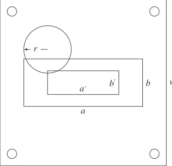
The antenna is designed for a resonant frequencyfr= 2.4 GHz. The structure of the proposed WCMPA is shown in Figure 1.
w
a
b a' b
'
r
Figure 1. Structure of WCMPA.
In the figure,landware outer dimensions of waveguide;aandbare inner dimensions of waveguide; a and b are dimensions of rectangular iris; r is the radius of the circular patch. There are four mounting holes to fix the antenna to the rectangular waveguide to feed the microwave signal. The iris dimensions [2, 3] are calculated using the equation given below.
a b
1−
λ
2a
2
= a b
1−
λ
2a
2
(3)
where wavelength is given by
λ= c
fr (4)
wherec is the speed of light andfr the resonant frequency.
The proposed antenna parameter specifications are given in Table 1.
Table 1. Antenna parametrs.
Parametrs Values
Outer dimensions of the waveguide 117×79 mm Inner dimensions of the waveguide 72.136×34.036 mm
Dimensions of the rectangular iris 57.83×27.23 mm Radius of the circular patch 17.34 mm
Resonant frequency 2.4 GHz Dielectric constant of the FR4 substrate 4.4
Thickness of the dielectric material 1.6 mm
3. ANALYSIS
acts as a filter and absorbs microwave energy and feed to the feed point. Method of moments is used for the analysis of this waveguide coupled microstrip antenna [10]. The total electric field on the waveguide coupled microstrip patch antenna is given by the following expression.
E=Ea+Es (5)
whereE is the total electric field,Ea is the applied electric field andEs is the scattered field. Because of infinite conductivity the tangential component of electric field is zero.
Etan= 0 =Ea+Es (6)
Here Ea and Es are due to vector and scalar potentials. The vector potential is due to the current density on the patch antenna and the scalar potential is due to the charges. The scattered electric field is given by the following equation.
Es=−jω AM(r)− ∇φM(r), (7)
r on S, where magnetic flux density is given by,
B =∇ ×A (8)
The scalar potential due to charges and vector potential due to current density are given by
φ(ρ) =
sGv(ρ)qs(ρ)ds (9)
A (ρ) =
sGA(ρ)
Js(ρ)ds (10)
Now the applied electric field is given by
Ea= (jω AM +∇φM)tan (11)
The general formula for method of moments [5] is given by
L(J) =V (12)
Here L is a linear operator representing the integro differential operator, J the unknown current distribution and V the voltage excitation. The current distribution in an antenna is the sum of a set ofN different current distributions or basis functions.
J = N
n−1
Infn(r) (13)
Here N is the total number of basis functions fn(r) and In the unknown weighting coefficient for the nth basis function. Hence the excitation voltage is given by
N
n−1
InL(fn(r)) =V (14)
The inner product is defined as
fm(r), fn(r)=
sfm(r)fn(r)ds (15)
wherefm(r) is the test function. Applying the inner product we get
N
n=1
Infm(r), L(fn(r))=fm(r), V) (16)
This equation can be written as
where
I = N
n=1
In (18)
V = fm(r), V (19)
Z =
N
n=1
fm(r), L(fn(r)) (20)
The testing function when applied to our patch we get the following equation
fmM ·Eads=jω s
fmM ·AMds− s(∇ ·
fmM)φMds (21)
According to Stokes theorem
s∇φM ·
fmMds=−
sφM(∇ ·
fmMds (22)
The vector potential is given by
AM(r) = μ0 4π s
JmMgds (23)
whereμ0 is the permeability in vacuum andg= exp−jkRR ,R=|r−r|is the free space Green’s function,
JM =Nn=1M InfnM. By substituting the value of JM inAM we get,
AM(r) = NM
n=1
μ0
4π sf M
m(r)gds
In (24)
Similarly scalar or electric potential is given by
φM(r) = 1 4π0 s
σMgds (25)
jωσM = −∇s·JM (26)
whereσM can be expressed as current density and hence electric potential becomes
φM(r) = NM n=1 1 4π0 j ω s∇ ·
fM(r)dsIn (27)
After applying the basis and testing functions, we can express in the following form. According to moments method, current distribution can be found from the matrix equation
NM
n=1
ZmnMMIn (28)
wherem= 1. . . NM,vmM =sfnM ·Eads.
In our present work, we use Matlab PDE toolbox for 2D generation of triangular mesh. Then using Delaunay function this mesh is converted into 3D form, and triangulation is obtained by the function trimesh. The area, center and edges of all the triangles are calculated [5, 6]. RWG basis functions of plus and minus triangles are calculated [7]. Edge lengths of common edges plus and minus triangles are also calculated. Using barycentric subdivision the plus and minus triangles are divided into 9 subtriangles. Using the edge length (subtriangle) centers of all 9 triangles are calculated. Then free vertexes of all plus and corresponding minus triangles are calculated by comparing all the three vertices of plus triangle with minus triangle. ρ+ and ρ− are obtained by taking the difference between free vertex and center
To find Z inner product expansion for both plus and minus triangles is given by the following expression.
s
fmMfnMgdsds = + lmln 4A+mA+n t+
m t+n
(ρ+m·ρn+)gdsds+ lmln 4A+mA−n t+
m t−n
(ρ+m·ρ−n)gdsds
+ lmln 4A−mA+n t−
m t+n
(ρ−m·ρn+)gdsds+ lmln 4A−mA−n t−
m t−n
(ρ−m·ρ−n)gdsds
s(∇. f M
m )(∇ ·fnM)gdsds = +4Alm+ln
mA+n t+
m t+n
gdsds+ lmln 4A+mA−n t+
m t−n
gdsds
+ lmln 4A−mA+n t−
m t+n
gdsds+ lmln 4A−mA−n t−
m t−n
gdsds
In this equation, the double integration is performed by summing the required values of all the triangles. Current is calculated by matrix inversion method. Now the impedance for different frequencies is calculated, and return loss graph is plotted. Radiation pattern is obtained by summing the currents of each triangle in different angles.
4. RESULT AND DISCUSSION
Figure 2 shows the simulated and measured plots of frequency verses return loss. The proposed waveguide fed antenna gives a bandwidth of 70% by simulation using matlab and 74.375% from vector network analyzer.
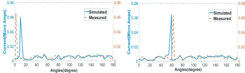
The 2D current distributions of the proposed antenna for different orientations of 0◦, 60◦, 90◦ and 120◦ are presented in Figures 3 and 4. The designed antenna is found to be very directional with narrow beamwidth in the given orientation of the radiating patch form the feeding point. The antenna
Figure 2. Comparison plot of frequency verses return loss.
Figure 4. Comparison plot of 2D current distribution for the patch orientations of 90◦ and 120◦.
Figure 5. Experimental setup of return loss and radiation pattern.
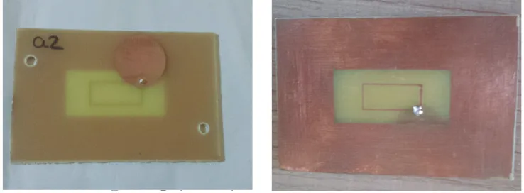
Figure 6. Radiating side and feeding side of proposed antenna.
is designed for an impedance of 50 Ω and provides 49.062 Ω impedance because of the iris structure inside the rectangular waveguide.
The experimental setup for measuring return loss using vector network analyzer and radiation pattern of proposed antenna are presented in Figure 5. Figure 6 shows the circular radiating side and waveguide feeding side of the designed waveguide coupled microstrip antenna.
ACKNOWLEDGMENT
REFERENCES
1. Balanis, C. A., Antenna Theory, Analysis and Design, John Wiley and Sons, New York, 1982. 2. Slater, J. C., Microwave Transmission, McGraw-Hill Book Company, New York, 1942.
3. Sisodia, M. L. and V. L. Gupta,Microwave Engineering, New Age International Publishers, 2005. 4. Engen, G. F. and R. W. Beatty, “Microwave reflectrometer technoques,” IRE Transactions on
Antenna and Propagation, 361–364, 1959.
5. Harrington, R. F., “Matrix methods for field problems,”IEEE Proc. Antennas Propagation, Vol. 55, No. 2, 136–149, Feb. 1967.
6. Makarov, S. N., “Matlab antenna toolbox — A draft,” web resource http://ece.wpi.edu/mom/, 2005.
7. Rao, S. M., D. R. Wilton, and A. W. Glisson, “Electromagnetic scattering by surfaces of arbitrary shape,” IEEE Trans. Antennas Propagat., Vol. 30, 409–418, 1982.
8. Pozar, D. M., Microwave Engineering, John Wiley and Sons, 2005.
9. Jose, S. K. and S. Suganthi, “Circular-rectangular microstrip antenna for wireless applications,” International Journal of Microwaves Applications, Vol. 4, 2015.