Available online: https://edupediapublications.org/journals/index.php/IJR/ P a g e | 3551
A single ended dynamic feedback control 8T sub threshold SRAM cell
Shaik.Khajabi, Miss. D Kamala Kumari
M.Tech Student, Assistant Professor
[email protected]. [email protected]
Nimra college of engineering and Technology
ABSTRACT: In this paper an 8T RAM cell with high information security that works on ULV is proposed. The proposed cell's zone is twice as that of 6T. The proposed 8T cell has high solidness and can be worked at ULV of 200–300 mV power supplies. The upside force utilization of the proposed 8T cell empowers that it should be utilized for battery worked SoC plan. Future and utilizations of the proposed 8T cell can possibly be in low/ULV and medium recurrence operation like neural sign processor, subthreshold processor, wide-working extent IA-32 processor, quick Fourier change centre, and low voltage reserve operation. At last it can be observed that proposed system gives better results compare to existed one.
KEY WORDS: 8T RAM Cell, ULV, RBL, RWL.
I.INTRODUCTION
The growing demand of portable battery operated systems has made energy efficient processors a necessity. For applications like wearable computing energy efficiency takes top most priority. These embedded systems need repeated charging of their batteries. The problem is more severe in the wireless sensor networks which are deployed for monitoring the environmental parameters. These systems may not have access for recharging of batteries. We know that on chip memories determine the power dissipation of SoC chips. Hence it is very important to have low power and energy efficient and stable SRAM which is mainly used for on chip memories.
There are various approaches that are adopted to reduce power dissipation, like design of circuits with power supply voltage scaling, power gating and drowsy method. Lower power supply voltage Reduces the dynamic power in quadratic fashion and leakage power in exponential
Way. But power supply voltage scaling results in reduced noise margin. Many SRAM arrays are based on minimizing the active capacitance and reducing the swing voltage. In sub-100nm region leakage currents are mainly due to gate leakage and sub threshold leakage current. High dielectric constant gate technology decreases the gate leakage current. Forward body biasing methods and dual Vt techniques are used to reduce sub threshold leakage current. The sub threshold of SRAMs is lower than the transistor threshold voltage (Vt). Now the sub threshold leakage current is the operating current.
Available online: https://edupediapublications.org/journals/index.php/IJR/ P a g e | 3552 SRAM is lost to ground in each write operation during ‘1’ to ‘0’ transition and this is the main source of energy loss. The power dissipated in bit lines represents about 60% of the total dynamic power consumption during a write operation. The power consumption by bit lines during writing is proportional to the bit line capacitance, square of the bit line voltage and the frequency of writing.
Energy loss is reduced by limiting voltage differences across conducting devices. This is accomplished through the use of time-varying voltage waveforms. This is also called Adiabatic charging technique. The SRAM working purely on adiabatic charging principles need multiple phase power clocks. Although there is huge saving in energy during writing as well as reading, the design of the SRAM circuit is complex and not same as the design of conventional SRAM. The latency of operation is more.
II. EXISTED SYSTEM
The convenient microchip controlled gadgets contain inserted memory, which speaks to a substantial part of the framework on chip (SoC). These convenient frameworks need ultralow power expending circuits to use battery for more term. The force utilization can be minimized by nonconventional gadget structures, new circuit topologies, and advancing the engineering. In spite of the fact that, voltage scaling has prompted circuit operation in sub limit administration with least power utilization, however there is a drawback of exponential lessening in execution. From below figure (1) we can observe the architecture of existed system.
The circuit operation in the sub threshold administration has cleared way toward ultra-low power inserted recollections, fundamentally static RAMs (SRAMs). Be that as it may, in sub threshold administration, the information steadiness of SRAM cell is a serious issue and declines with the scaling of MOSFET to sub nanometre Technology. Because of these impediments it gets to be hard to work the traditional 6-transistor (6T) cell at ultralow voltage (ULV) power supply. The essential and a successful approach to dispose of this issue is the decoupling of genuine putting away hub from the bit lines amid the read operation.
This read decoupling methodology is used by ordinary 8-transistor [read decoupled 8- transistor (RD-8T) cell which offers read static commotion edge (RSNM) equivalent withhold static clamour edge (HSNM). Be that as it may, RD8T experiences spillage
Available online: https://edupediapublications.org/journals/index.php/IJR/ P a g e | 3553 presented in read way. This spillage current increments with the scaling consequently, expanding the likelihood of fizzled read/compose operations. Comparative the cells will keep the cell current without aggravating the capacity hub as additionally.
III. PROPOSED SYSTEM
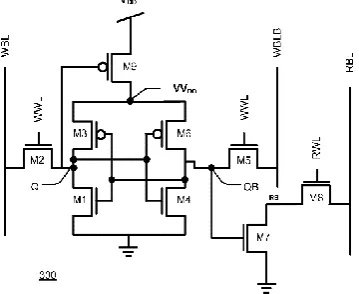
Single-finished with element criticism control cell is displayed to make a cell stable in all operations, as shown in Figure (2). The single-finished configuration is utilized to decrease the differential exchanging power and read–write operation. The force expended and exchanging/flipping of information on single piece line is lesser than that on differential bit-line pair. The RAMempowers composing through single nMOS in 8T. It likewise isolates the read and composes way and displays read decoupling. The basic change of cell is considered to upgrade the safety against the process–voltage– temperature (PVT) varieties.
It enhances the static clamor edge (SNM) of 8T cell in sub threshold/close edge area. The proposed 8T has one cross-coupled inverter pair, in which every inverter is comprised of three fell transistors. These two stacked cross-coupled inverters: M1–M2–M4 and M8–M6– M5 hold the information amid hold mode. The compose word line (WWL) controls one and only nMOS transistor M7, used to exchange the information from single compose bit line (WBL). A different read bit line (RBL) is used to exchange the information from cell to the yield when perused word line (RWL) is initiated. Two segments one-sided criticism control signals: FCS1 and FCS2 lines are utilized to control the input cutting transistors: M6 and M2, individually.
1) Cell Layout: For examination of region, format of 5T, 6T, RD-8T, and proposed 8T are
attracted UMC 90-nm CMOS innovation. The sizes of MOSFETs utilized as a part of proposed 8T cell are delineated. The RD-8T involves 1.3× range as contrasted and that of 6T. Because of the configuration limitations and contact region between M2, M3, M4, and M8 the 2 × zones will be contrasted on 6T cell.
2) WriteOperation: The criticism slicing plan is utilized to compose into 8T. In this plan,
amid compose 1 operation FCS1 is made low which switches OFF M6. At the point when the RWL is made low and FCS2 high, M2 conducts associating Complementary Q (QB) to the ground. Presently, if the information connected to word bit line (WBL) is 1 and WWL is actuated, then current streams from WBL to Q and makes a voltage trek on Q by means of M7-composing 1 into the cell.
3) Read Operation: The read operation is performed by precharging the RBL and enacting
RWL. On the off chance that 1 is put away at hub Q then, M4 turns ON and makes a low resistive way for the stream of cell current through RBL to ground. This releases RBL
Available online: https://edupediapublications.org/journals/index.php/IJR/ P a g e | 3554 rapidly to ground, which can be detected by the full swing inverter sense intensifier. Since WWL, FCS1, and FCS2 were made low amid the read operation
4) Half-Selected Issue: At whatever point a cell is chosen for compose operation, the
voltage of genuine stockpiling hub (Q) of line half-chose cells will ascend because of charge exchange from WBL. The reciprocal stockpiling hub QB does not have solid association with the bit line (RWL is OFF) and in this way, less opportunities to flip the cell as com-pared with traditional 6T/RD-8T cell. This can be checked by 1000 Monte Carlo (MC) re-enactments, as appeared.
IV. RESULTS
LAYOUT IN MICROWIND
LAYOUT OUTPUT
DRAIN VOLTAGE VS CURRENT
V. CONCLUSION
Available online: https://edupediapublications.org/journals/index.php/IJR/ P a g e | 3555 proposed 8T cell empowers it to be utilized for battery worked SoC plan. So at last it can conclude that the proposed system gives better efficiency compared to exist one.
VI. REFERENCES
[1]K. Roy and S. Prasad, Low-Power CMOS VLSI Circuit Design, 1st ed. New York, NY, USA: Wiley, 2000.
[2]N. Verma and A. P. Chandrakasan, “A 256 kb 65 nm 8T subthreshold SRAM employing sense-amplifier redundancy,” IEEE J. Solid-StateCircuits, vol. 43, no. 1, pp. 141–149, Jan. 2008.
[3]C. Kushwah and S. K. Vishvakarma, “Ultra-low power sub-threshold SRAM cell design to improve read static noise margin,” in Progress inVLSI Design and Test (Lecture Notes in Computer Science), vol. 7373.Berlin, Germany: Springer-Verlag, 2012, pp. 139–146.
[4]B. H. Calhoun and A. P. Chandrakasan, “A 256-kb 65-nm sub-threshold SRAM design for ultra-lowvoltage operation,” IEEE J. Solid-StateCircuits, vol. 42, no. 3, pp. 680–688, Mar. 2007.
[5]C. B. Kushwah, D. Dwivedi, and N. Sathisha, “8T based SRAM cell and related method,” U.S. Patent IN920 130 218 US1, May 30, 2013.