Directive and Reconfigurable Loaded Antenna Array for Wireless
Sensor Networks
Akimu Dihissou*, Aliou Diallo, Philippe Le Thuc, and Robert Staraj
Abstract—In this paper, a four switchable beam antenna dedicated to Wireless Sensor Network (WSN) nodes in the 2.4 ISM band (2.4–2.485 GHz) is presented. It consists of two fed monopoles and two loaded parasitic ones. The nature and value of the load are obtained using the Uzkov equations, allowing to determine current weighting coefficients in the case of two separately fed antennas, in order to maximize the gain and the directivity in a given direction. Reconfigurability is achieved using reflector and director elements activated by PIN diodes to reduce the back radiation and pointing in the desired direction. Thus, a first system is obtained which consists of two elements, one fed and the other loaded with an inductor, with a maximum gain of 5.2 dBi in simulation and 4.7 dBi measured at 2.4 GHz in azimuthal directions of 90◦ and 270◦. Then, the system is compared with another, composed of two antennas fed separately. Finally, the same methodology is applied to an array of four antennas, in which two antennas are fed, and two are loaded. This last structure is capable of steering its radiation pattern in the azimuth plane, covering a 360◦ angle with four beams (0◦, 90◦, 180◦ and 270◦). The total gain achieved is 4 dBi for each beam in the azimuth plane.
1. INTRODUCTION
Today’s high rates of data communication are continually increasing, along with the number of devices connected to mobile networks, especially in the domain of wireless sensor networks (WSNs). These devices are valuable and effective since they provide a powerful combination of distributed sensing, computing, and communication resources using other devices to gather information for decision making [1]. Their applications range from military surveillance, in which many sensor nodes are used, to health-care applications, in which a very limited number of sensor nodes are used [2].
Although WSNs are very useful, they have several shortcomings. The main issue is their limited battery life, in many applications, the energy module cannot be replaced. Since communication is the most power-consuming task, it is important to achieve energy-efficient communication in order to increase the lifetime of the devices through a careful use of power transmission [3].
One promising solution for overcoming this issue is the use of a directive and reconfigurable antenna design at the hardware level of the sensor node [4, 5]. This permits a significant reduction in collision and interference packets [6, 7]. Moreover, it can help to extend the range of communication between nodes, allowing the possibility of using a smaller number of nodes within the monitoring area.
Few solutions specifically dedicated to WSNs have been proposed thus far, and these are typically limited in terms of high directivity. Cubic and loop antenna designs, presented by Kruesi et al. [8] and Genovesi et al. [9], respectively, offer omnidirectional and bidirectional patterns that can cause collision and interference between packets. Moreover, these beam patterns are not switchable. Hence, the designs are unsuitable for a random deployment of nodes in the azimuth plane, which is the preferred plane for communications with nodes scattered on the ground. Hwang et al. [10] has proposed a
Received 24 March 2018, Accepted 13 May 2018, Scheduled 24 May 2018
* Corresponding author: Akimu Dihissou ([email protected]).
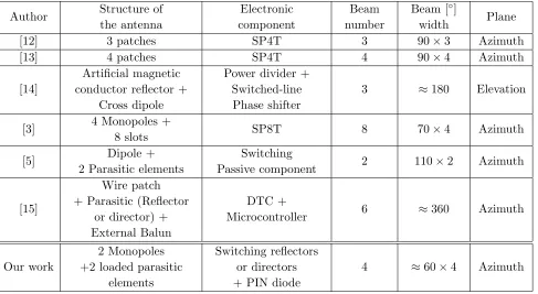
switched beam antenna composed of an artificial magnetic conductor reflector, two branched radiators and a power divider including a switched-line phase shifter. It is capable of switching between a side directional pattern and a normal directional pattern. Unfortunately, it does not offer a radiating beam in the azimuth plane, although it achieves a substantial peak gain. Another switched antenna has been presented by Mottola et al. [11]. This covers all directions via a switch control; however, it does not present a narrow beam in the azimuth plane, which may create an overlapping area for energy-saving purposes. The solution proposed in this article can also be compared to those presented by Yang et al. [12], Giorgetti et al. [13], Kim et al. [14], Catarinucci et al. [3], Barousis et al. [5], Lizzi et al. [15] and listed in Table 1. All these antennas can be reconfigured in terms of radiation pattern using electronic components such as switches, PIN diodes, Digitally Tuned Capacitors (DTCs), .... However, these antennas suffer from a too wide beamwidth. The directive and reconfigurable antenna presented in this paper proposes a solution to improve its beam directivities.
Table 1. Comparison of reconfigurable antenna solutions for WSN.
Author Structure of the antenna
Electronic component
Beam number
Beam [◦]
width Plane
[12] 3 patches SP4T 3 90×3 Azimuth
[13] 4 patches SP4T 4 90×4 Azimuth
[14]
Artificial magnetic conductor reflector +
Cross dipole
Power divider + Switched-line Phase shifter
3 ≈180 Elevation
[3] 4 Monopoles +
8 slots SP8T 8 70×4 Azimuth
[5] Dipole +
2 Parasitic elements
Switching
Passive component 2 110×2 Azimuth
[15]
Wire patch + Parasitic (Reflector
or director) + External Balun
DTC +
Microcontroller 6 ≈360 Azimuth
Our work
2 Monopoles +2 loaded parasitic
elements
Switching reflectors or directors + PIN diode
4 ≈60×4 Azimuth
Another solution not limited in terms of directivity has also been proposed for WSNs, the phased array. In fact, phased array is a collection of antennas that are mostly spaced evenly along one direction or in a two-directional for bi-dimensional arrays. Hence, by adjusting the number of antenna elements, geometric placement, amplitudes and phases of the antenna elements, the desired radiation pattern can be produced [16].
Nevertheless, this solution appears more complex for the nodes in our possession [17] in that it may require a phase and amplitude controller circuit in their implementation.
The paper is organized as follows. First, we present the initial structure. It is an array made up of two printed monopoles designed with the help of the commercial software ANSYS HFSS. Following this, a technique which allows improvement in the gain or the directivity of this array is described. Then, the modification of one of the monopoles into a loaded parasitic element is presented [23], where only two opposite beams were achieved. Subsequently, an application of this technique is applied to a combination of two fed and parasitic element arrays. Finally, both simulated and experimental results are presented to validate our solution.
2. DESIGN AND STRUCTURE OF THE ANTENNA
The first proposed array is etched on a 1.524 mm-thick Rogers RO4003 substrate with a relative permittivity of 3.32 and a loss tangent of 0.0027. Each antenna is a fed printed monopole, aligned along the Z-axis on the top of the substrate (Fig. 1). The dimensions l×w of the fed monopole are 35×5 mm2, which correspond to 0.28λ0×0.04λ0 for a central frequency off0 = 2.45 GHz. The values
of width w and length l were tuned at f0 using the commercial software HFSS, provided by ANSYS.
The notch width S, the transmission line length t and its width were set to 2 mm, 3 mm and 1 mm respectively. This kind of geometry easily facilitates the input impedance matching while keeping a symmetry in the radiation pattern. The distance between the symmetrical (with respect to theY-axis in this array) feeding ports P1 and P2 is set to 0.08λ0 as seen in Fig. 2(a). On the other face of the
substrate lies a circular ground plane (of radius 15 mm) and six identical rectangular stubs (29×5 mm2) arranged symmetrically with respect to theY axis. These six stubs are divided into two groups: stubs 1 to 3 and stubs 4 to 6.
Figure 1. Geometry of one radiating element.
(a) (b) (c)
Figure 2. Geometry of the antenna array. (a) Top view. (b) Bottom view for mode I. (c) Bottom view for mode II.
The ground plane may or may not be directly connected to a group of three stubs via a set of three identical PIN diodes (D1,D2,D3) or (D4,D5,D6) as shown in Figs. 2(b) and 2(c). This configuration
allows the radiation patterns to be changed in the azimuth plane, XZ; this is the preferred plane for communication with nodes scattered on the ground. The set of PIN diodes (D1 to D3) and (D4 to
D6), are used to alter the beam directions at 270◦ (mode I) (Fig. 2(b)) and 90◦ (mode II) (Fig. 2(c))
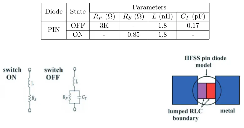
E6327 by Infineon, which operates up to 6 GHz; its equivalent circuit model for OFF and ON states [24] are shown in Fig. 3.
The parameter values of the equivalent circuit model are given in Table 2 corresponding to the datasheet of the PIN diode used. The resistorRP and capacitanceCT values are not defined in the ON state. Likewise, the resistorRS is not defined in the OFF state.
Table 2. Parameter values of the PIN diode equivalent circuit at 1 GHz.
Diode State Parameters
RP (Ω) RS (Ω) L (nH) CT (pF)
PIN OFF 3K - 1.8 0.17
ON - 0.85 1.8
-Figure 3. Equivalent circuit of the BAR64-03W E6327 PIN diode by Infineon.
Figure 4. RF PIN diode modelled in HFSS.
The PIN diode is modelled in HFSS using two series lumped boundary conditions [24], as shown in Fig. 4. The bias circuit diagram of the antenna array is depicted in Fig. 5, with its bias network value presented in Table 3. To protect the PIN diode from damage, a series resistor of 100 Ohms is integrated on each static polarization line.
Table 3. Bias voltage and the corresponding activation of PIN diodes.
V (V) Mode D1 D2 D3 D4 D5 D6
0.8 1 On On On Off Off Off
−0.8 2 Off Off Off On On On
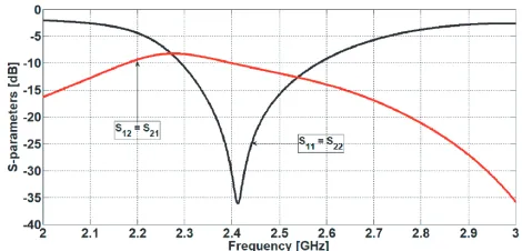
The objective is to cover the 2.4-ISM band (2.4–2.485 GHz) with a matching criterion of reflection coefficients Sii lower than −10 dB. Regardless of the excitation of each antenna and the activation set of modes I or II, the antenna array provides an identical reflection coefficient due to the symmetrical nature of the structure. A reflection coefficient lower than−15 dB and an isolation around 10 dB in the 2.4-ISM band are observed, as shown in Fig. 6. As for the radiation performance, when antennaAnt2is
not excited but is loaded by 50 Ohms, antenna Ant1 is excited with P1 (1 W, 0◦) due to the activation
of PIN diodes in mode I; simulated realized total gain values of 3.1 dB around the −X direction and 2.5 dB in−Z direction are reached respectively, as shown in Fig. 7. Furthermore, when the first antenna Ant1 is not excited but is loaded by 50 Ohms, the second antenna Ant2 is excited with P2 (1 W, 0◦)
Figure 5. Bias circuit diagram of the proposed antenna.
Figure 6. Simulated reflection and isolation coefficients of the two-monopole array.
Figure 7. Simulated realized total gain in the azimuth plane xz of the two monopole-array: mode I (green line) and mode II (grey line).
3. DIRECTIVITY ENHANCEMENT
To improve both the gain and directivity of this array, the value of the excitation coefficient that maximizes these parameters in the direction (θ0, ϕ0) is required [18, 25, 26]. Hence in our approach, the
beam is oriented in the desired direction according to the selected set of PIN diodes (D1 toD3) or (D4
toD6). We first select the set of PIN diodes (D1,D2,D3) (mode I). The antennaAnt1 is excited with
P1 (1 W, 0◦) while varying either the amplitude or phase of the feeding port of Ant2 corresponding to
a variation of the power ratio P1/P2. Then, we vary the amplitude of the feeding port of Ant2 from
0 W to 1 W with a fixed phase of 180◦. Following this, we vary the phase of the feeding port of Ant2
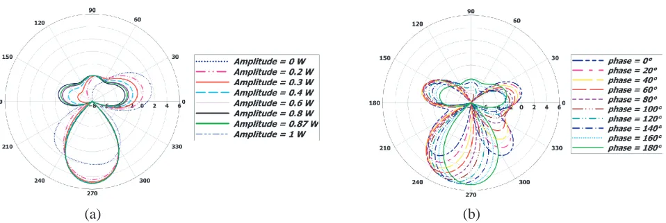
from 0◦ to 180◦ with a fixed amplitude of 0.87 W. Finally, the simulated directivity patterns for the given values of the amplitude and phase of Ant1 and Ant2 are plotted in Fig. 8. We can observe that
as the amplitude of the feeding port of Ant2 increases, the directivity corresponding to mode I in the
backward direction decreases and those in the forward direction increase. Moreover, as the phase of the feeding port ofAnt2 is increased, the directivity (mode I) in the backward direction decreases and that
in the forward direction increases. It can then be observed that the highest value of directivity with the lowest directivity in the backward direction corresponds to an applied power excitation of 0.87 W and phase of 180◦.
These values can be assessed using the methodology of excitation coefficients proposed in [27, 28] and the Uzkov equations [29] given by the following relations:
(a) (b)
Figure 8. Simulated directivity in the azimuth plane (xz) of the two monopoles array. (a) Variation of the directivity as a function of the amplitude of the feeding port P2 with a fixed phase equals to 180◦.
(b) Variation of the directivity as a function of the phase of the feeding portP2 with a fixed amplitude
equals to 0.87 W.
Figure 9. Simulated realized total gain in the azimuth plane of the two monopoles array. Mode I (green line) and mode II (grey line).
H12 =
1 4π
2π ∑
θ=0
π ∑
ϕ=0
f1(θ, ϕ)f2∗(θ, ϕ)ejkrˆ(r2−r1)×sin(θ)∆(θ)∆(ϕ) (2)
f1 = Eθ1 +Eϕ1 (3)
f2 = Eθ2 +Eϕ2 (4)
where a02 is the current ratio between the feeding ports and can be expressed according to the power
ratio P1/P2 and the Z-parameters; H12 is obtained from the Uzkov equation; k = ω/c is the wave
number; ˆr0 is the unit vector in the far-field direction (θ0,ϕ0);r2 is the feeding port positionP2 of the
second antenna with respect to a fixed rectangular (xyz) coordinate system;f1 andf2 are the radiated
electrical fields in the far field direction (θ, ϕ); ˆr is the unit vector in the far-field direction (θ, ϕ); r2−r1 is the distance between the feeding port positionsP2 andP1 of the antennas; ∆(θ) = 2π/Nθ and ∆(ϕ) = 2π/Nϕare the far-field sampling steps in the spherical angles (θ,ϕ), where Nθ andNϕare the number of samples.
The values of P1 (1 W, 0◦) and P2 (0.87 W, 180◦) are then used to excite each feed respectively.
Hence, when Ant1 is excited withP1 (1 W, 0◦) whileAnt2 is excited withP2 (0.87 W, 180◦) in mode I,
a simulated realized total gain of 5.5 dB is achieved in the 270◦ direction. The back radiation is then equal to −2.3 dB as seen in Fig. 9. When Ant1 is still excited withP1 (1 W, 0◦) while Ant2 is excited
withP2 (0.87 W, 180◦) and the mode II is activated, a simulated realized total gain of 5.5 dB is achieved
in the 90◦ direction. The back radiation is −2.3 dB, as also shown in Fig. 9. It can be seen that an improvement of 2.5 dB is obtained in both the 270◦ and 90◦ directions corresponding to the X-axis. Moreover, the second beam is removed compared to the previous simulated radiation patterns. In this case, the directional and reflector aspects of the stubs used at the bottom of the substrate are improved.
4. DESIGN AND STRUCTURE OF THE PARASITIC ANTENNA
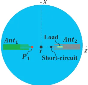
The introduction of a weighting coefficient for the amplitudes and phases of the injected powers for each antenna may be achieved using a single fed port by adding a power divider and a phase shifter circuit, both of which are reconfigurable in the system. However, this solution would produce a more complex system. To avoid this, one of the monopoles is modified into a loaded parasitic element fed by coupling. Hence, only one of the two monopoles (Ant2 in this case) is loaded with a passive component and its
feedP2 becomes a short circuit, as shown in Fig. 10. Fig. 11 illustrates the top view of the structure of
the fed monopole (Ant1) and the loaded parasitic monopole.
Figure 10. Parasitic antenna with a load. Figure 11. Top view of the new antenna array.
The required load is thoroughly carried out using Eqs. (5) and (6) as described in [30].
Zactive(2) =
V2
I2
=Z22+Z21×
I1
I2
(5)
Zload(2) = −Zactive(2) (6)
where V2 and I2 define the input voltage and current of the second antenna. The Zii parameters are derived from [Z], the array impedance matrix, and the current ratio represents the excitation coefficient a02. The nature of the required load is found to be an inductance with a value of 9.6 nH. With this
value, almost equivalent directivity will be attained as in the approach described in [18–21, 31]. In the work presented by Harrington in [31], variable reactance loads provide a mean for beam steering. In contrast to our work, once the required load is found, the beam steering is achieved by the use of PIN diodes.
As can be observed, there is a shift in the reflection coefficient curves between the simulation and the measurement. This shift cannot only be attributed to the values of the components taking into account the equivalent model of the PIN diode given for a frequency of 1 GHz in the datasheet. However, it can also come from the incertitudes of manufacturing and the exact value of the relative permittivity of the substrate. In fact, for the used substrate, the manufacturer does provide a relative permittivity range from 3.33 to 3.43. Our simulations were run with the default value of the relative permittivity given by ANSYS HFSS. Nevertheless, both the measured and simulated reflection coefficients are −17.6 dB at 2.4 GHz. Good agreement is seen between the curves of the modes, due to the symmetrical nature of the antenna system.
(a) (b)
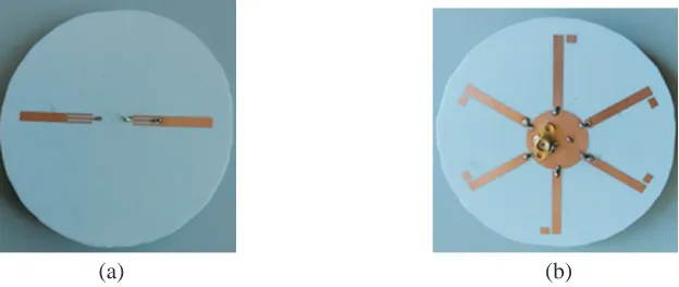
Figure 12. Prototype of the transformed monopole array antenna. (a) Top view. (b) Bottom view.
Figure 13. Simulated (solid line) and measured (dotted line) results for the reflection coefficient.
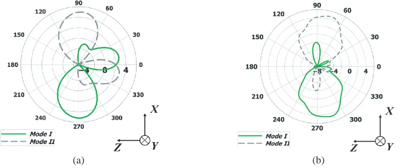
When the fed monopole is excited with P1 (1 W, 0◦) and mode I activated, a simulated realized
total gain of 5.2 dB is achieved in the 270◦ direction, as shown in Fig. 14(a); in experiment, this value is 4.7 dB (Fig. 14(b)). However, when mode II is activated, the same simulated and measured values are obtained (Fig. 14(a) and Fig. 14(b)). This highlights the relevant role of the reflectors, as described above. The measured total radiation efficiency is 56.9% for both modes I and II at 2.4 GHz. The decrease in the measured peak gain is due to the PIN diode losses; indeed, the insertion loss of each PIN diode is 0.16 dB. A secondary lobe is noticed in simulation compared to experiment, since the component values given by the datasheet for the PIN diode equivalent model are only valid below 1 GHz as discussed above even though this diode can be used up to 6 GHz. Thus at these values, the PIN diodes do not behave like perfect short-circuit at the frequency of 2.4 GHz. Fig. 15 shows a 3D view of the radiation pattern simulated for each mode in the azimuth plane.
5. DESIGN AND STRUCTURE OF THE FINAL ANTENNA STRUCTURE
(a) (b)
Figure 14. Simulated and measured realized total gains at 2.4 GHz. (a) Simulated pattern. (b) Measured pattern.
(a) (b)
Figure 15. 3D view of the simulated total gain of the parasitic loaded antenna. (a) Mode I. (b) Mode II.
antennasAnt1 and Ant2 are obtained. Each radiating element has its own feeding port, that is,P1 and
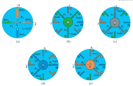
P2 for Ant1 and Ant2 respectively. Then, two parasitic monopole antennas (Antp1 and Antp2) loaded with the same passive component are also obtained. Their feeding ports have been short-circuited to the ground plane located underneath the substrate. Furthermore, eight identical rectangular stubs symmetrically arranged with respect to theY axis and separated from each other at 45◦, are added on the lower face of the substrate. These eight stubs are divided into four groups: stubs 1 to 3; stubs 4 to 6; and stubs 2, 5 and 7; and stubs 3, 6 and 8. Fig. 16 depicts the antenna configurations.
The excitation mechanism of this final antenna is as follows:
• When Ant1 is excited with P1 (1 W, 0◦), Ant2 is loaded with 50 Ohms. In this case, two beams
in the azimuth plane are observed, depending on the activation set of PIN diodes. The sets of PIN diodes (D1 to D3) and (D4 to D6), are used to alter the beam directions at 270◦ (mode I)
(Fig. 16(b)) and, 90◦ (mode II) (Fig. 16(c)) respectively.
• When Ant2 is excited with P2 (1 W, 0◦), and Ant1 is loaded with 50 Ohms, two other beams in
the azimuth plane are also observed. The sets of PIN diodes (D2, D5, D7) and (D3,D6, D8) are
used to alter the beam directions at 0◦ (mode III) (Fig. 16(d)) and, 180◦ (mode IV) (Fig. 16(e)) respectively.
(a) (b) (c)
(d) (e)
Figure 16. Geometry of the parasitic antenna. (a) Top view. (b) Bottom view for mode I. (c) Bottom view for mode II. (d) Bottom view for mode III. (e) Bottom view for mode IV.
Figure 17. Simulated S-parameters correspond-ing to mode I.
Figure 18. Simulated S-parameters correspond-ing to mode II.
(a) (b)
Figure 20. Simulated S-parameters with neutralization line.
(a) (b)
Figure 21. Prototype of the final antenna. (a) Top view. (b) Bottom view.
Figure 22. S-parameters corresponding to mode I.
Figure 23. S-parameters corresponding to mode II.
Figure 24. S-parameters corresponding to mode III.
(a) (b) (c)
Figure 26. Prototype under test. (a) 3D radiation setup. (b) Top view face. (c) Bottom view face.
(a) (b)
(c) (d)
Figure 27. Simulated (solid line) and measured (dash line) realized total gain at 2.4 GHz for the four modes. (a) Mode I. (b) Mode II. (c) Mode III. (d) Mode IV.
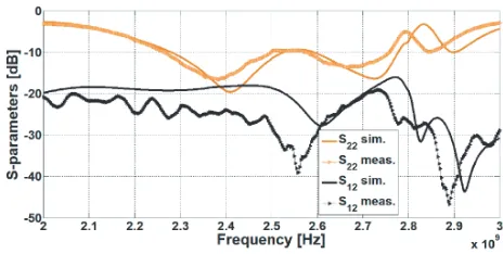
The simulated reflection coefficient,S11, is smaller than −10 dB in the desired frequency band for
both modes I and II. However, a difference is seen in their isolations as described byS12. For mode I, the
band.
To maximize the energy radiated byAnt1, we must ensure that its energy is effectively transmitted
rather than being lost in the second antennaAnt2, which is simultaneously loaded with 50 Ohms. We
must therefore maximize the isolation between the two feeding ports of the antennas for each mode. Hence, a neutralization lines [32, 33] including a capacitive effect has been added to the top view of the design, as shown in Fig. 19(a) without affecting the radiation pattern of each state. As a result, an isolation greater than 10 dB is obtained (Fig. 20). However, by cutting off this line in two identical parts with a spacing of 0.2 mm, as shown in Fig. 19(b), the isolation value is enhanced (higher than 10 dB) as depicted in (Fig. 20).
The section of this neutralization line spaced by 0.2 mm is then maintained to plot the simulated and measured S parameters for the four operational modes as shown in Figs. 22 to 25. In Figs. 22 and 23 corresponding to modes I and II, we are interested in Ant1. The reflection coefficient, S11, is
smaller than −10 dB in the desired frequency band for both simulation and experiment. In addition, the isolation, described by S21, is greater than 12 dB. In Figs. 24 and 25 corresponding to modes III
and IV, we are interested inAnt2. The reflection coefficient, S22, is smaller than −10 dB in the desired
frequency band for both simulation and measurement. In addition, the isolation, S21, is greater than
12 dB.
Figure 21 depicts the prototype fed by two 50 Ohm-mini-coaxial cables.
The far-field azimuth patterns of the prototype were measured at 2.4 GHz using a LEAT 3D radiation setup (Fig. 26). This 3D radiation setup is able to take samples of the electromagnetic near field from a moving measurement probe on a spherical surface surrounding the prototype under test. Then a software allows the reconstruction of the distribution of the electromagnetic far field.
Figure 27 illustrates the simulated and measured far-field azimuth patterns at 2.4 GHz for the four states. In all cases, the simulated and measured peak realized total gain is close to 4 dBi. The simulated 3-dB beamwidth of the azimuth patterns for the four states are all about 60◦, demonstrating that the proposed antenna has good directional radiation performance. This also highlights the key role of stubs 1, 4, 7 and 8 acting as directors. The total radiation efficiency for four states at 2.4 GHz is about 54% in measurement including the PIN diodes.
6. CONCLUSION
In this paper, a four-switched beam antenna was proposed. We first described improvements in the gain and the directivity of an array of two fed monopoles. The excitation value for each feeding port was thoroughly investigated in order to achieve a high gain in the direction of each director. Then, thanks to the use of a set of PIN diodes, one of these two directions can be selected, which allows a reconfigurable radiation pattern. Following this, this array is transformed by loading one of the two monopoles with an inductive load. The load value was found to achieve almost the same performance as the simulated results in the first case while maintaining the reconfigurable capability. The proposed structure combines the technic of super directivity using loaded parasitic elements, switching reflector and director elements showing the novelty of this work. Finally, to cover more directions in the azimuthal plane, two identical elements are orthogonally added, and a four-switched beam antenna is obtained. In effect, this enables coverage of the same number of directions, but by using only two feeding ports instead of four. In order to enhance the isolation between them, two neutralization lines were implemented. The experimental results show that the proposed designs are suitable for WSN applications needing reconfigurable radiation patterns.
ACKNOWLEDGMENT
REFERENCES
1. Puccinelli, D. and M. Haenggi, “Wireless sensor networks: Applications and challenges of ubiquitous sensing,”IEEE Circuits and Systems Magazine, Vol. 5, No. 3, 19–31, 2005.
2. Ceclio, J. and P. Furtado, Wireless Sensors in Heterogeneous Networked Systems, Springer, 2014. 3. Catarinucci, L., S. Guglielmi, R. Colella, and L. Tarricone, “Compact switched-beam antennas
enabling novel power-efficient wireless sensor networks,” IEEE Sensors Journal, Vol. 14, No. 9, 3252–3259, September 2013.
4. Anastasi, G., M. Conti, D. M. Francesco, and A. Passarella, “Energy conservation in wireless sensor networks: A survey,” Ad Hoc Networks, Vol. 7, No. 3, 537–568, 2009.
5. Barousis, V. I., E. Roumpakias, and C. B. Papadias, “A parasitic antenna array for directive multi-hop sensor communication,”IEEE 14th Workshop on Signal Processing Advances in Wireless Communications (SPAWC), 500–504, June 2013.
6. Le, T. N., A. Pegatoquet, T. Le Huy, L. Lizzi, and F. Ferrero, “Improving energy efficiency of mobile WSN using reconfigurable directional antennas,” IEEE Communications Letters, Vol. 20, No. 6, 1243–1246, June 2016.
7. Joshi, G. P., S. Y. Nam, and S. W. Kim, “Cognitive radio wireless sensor networks: Applications, challenges and research trends,” Sensors, Vol. 13, No. 9, 11196–11228, 2013.
8. Kruesi, C. M., R. J. Vyas, and M. M. Tentzeris, “Design and development of a novel 3-D cubic antenna for wireless sensor networks (WSNs) and RFID applications,” IEEE Trans. Antennas Propag., Vol. 57, No. 10, 3293–3299, October 2009.
9. Genovesi, S., S. Saponara, and A. Monorchio, “Parametric design of compact dual-frequency antennas for wireless sensor networks,”IEEE Trans. Antennas Propag., Vol. 59, No. 7, 2619–2627, July 2011.
10. Hwang, K. S., J. Ahn, K. J. Kim, H. K. Yoon, and Y. J. Yoon, “Pattern reconfigurable antenna for a wireless sensor network sink node,”Asia-Pacific Microwave Conference, Vol. 59, No. 7, 2021–2024, December 2010.
11. Mottola, L., T. Voigt, and G. P. Picco, “Electronically-switched directional antennas for wireless sensor networks: A full-stack evaluation,” IEEE International Conference on Sensing, Communications and Networking (SECON), 176–184, June 2013.
12. Yang, C.-L., J. F. Mastarone, and W. J. Chappell, “Directional antennas for angular diversity in wireless sensor networks,” IEEE Antennas and Propagation Society International Symposium, Vol. 4A, 263–266, July 2005.
13. Giorgetti, G., A. Cidronali, S. K. S. Gupta, and G. Manes, “Exploiting low-cost directional antennas in 2.4 GHz IEEE 802.15.4 wireless sensor networks,” European Conference on Wireless Technologies, 217–220, October 2007.
14. Kim, K., K. Hwang, J. Ahn, and Y. Yoon, “Pattern reconfigurable antenna for wireless sensor network system,”Electronics Letters, Vol. 48, No. 16, 984–985, August 2012.
15. Lizzi, L., F. Ferrero, J. M. Ribero, R. Staraj, T. N. Le, A. Pegatoquet, and L. H. Trinh, “Differential pattern-reconfigurable antenna prototype for efficient wireless sensor networks,”IEEE International Symposium on Antennas and Propagation, 1239–1240, June 2016.
16. Huang, R. and Y. Manoli, “Phased array and adaptive antenna transceivers in wireless sensor networks,”Euromicro Symposium on Digital System Design, 587–592, August 2004.
17. “PowWow Hardware Platform,” http://powwow.gforge.inria.fr/subpages/Hardware.html.
18. O’Donnell, T. H. and A. D. Yaghjian, “Electrically small superdirective arrays using parasitic elements,” IEEE Antennas and Propagation Society International Symposium, 3111–3114, July 2006.
19. Haskou, A., A. Sharaiha, and S. Collardey, “Design of small parasitic loaded superdirective end-fire antenna arrays,”IEEE Trans. Antennas Propag., Vol. 63, No. 12, 5456–5464, December 2015. 20. Clemente, A., C. Jouanlanne, and C. Delaveaud, “Analysis and design of a four-element
Propagation (EUCAP), 2700–2704, March 2017.
21. Sentucq, B., A. Sharaiha, and S. Collardey, “Superdirective compact parasitic array of metamaterial-inspired electrically small antenna,”International Workshop on Antennas Technology (iWAT), 269–272, March 2013.
22. Dihissou, A., A. Diallo, P. Le Thuc, and R. Staraj, “Antenne directive et reconfigurable pour r´eseau de capteurs sans fil,” 19`emes Journ´ees Nationales Microondes (JNM 2015), June 2015.
23. Dihissou, A., A. Diallo, P. Le Thuc, and R. Staraj, “Technique to increase directivity of a reconfigurable array antenna for wireless sensor network,” 11th European Conference on Antennas and Propagation (EUCAP), 606–610, March 2017.
24. Nasrabadi, E. and P. Rezaei, “A novel design of reconfigurable monopole antenna with switchable triple band-rejection for UWB applications,” International Journal of Microwave and Wireless Technologies, Vol. 8, No. 8, 1223–1229, 2016.
25. Boyle, K., “Radiation patterns and correlation of closely spaced linear antennas,” IEEE Trans. Antennas Propag., Vol. 50, No. 8, 1162–1165, August 2002.
26. Mazinani, S. M. and H. R. Hassani, “Two element wideband Planar plate monopole superdirective array,”18th Iranian Conference on Electrical Engineering, 80–85, May 2010.
27. Haskou, A., A. Sharaiha, S. Collardey, M. Pigeon, and K. Mahdjoubi, “A design methodology for electrically small superdirective antenna arrays,” Loughborough Antennas and Propagation Conference (LAPC), 405–409, November 2014.
28. Haskou, A., A. Sharaiha, and S. Collardey, “Integrating superdirective electrically small antenna arrays in PCBs,”IEEE Antennas Wireless Propag. Lett., Vol. 15, 24–27, 2016.
29. Altshuler, E. E., T. H. O’Donnell, A. D. Yaghjian, and S. R. Best, “A monopole superdirective array,”IEEE Trans. Antennas Propag., Vol. 53, No. 8, 2653–2661, August 2005.
30. Balanis, C. A.,Antenna Theory: Analysis and Design, Wiley-Interscience, 2005.
31. Harrington, R., “Reactively controlled directive arrays,” IEEE Trans. Antennas Propag., Vol. 26, No. 3, 390–395, May 1978.
32. Diallo, A., C. Luxey, P. Le Thuc, R. Staraj, and G. Kossiavas, “Study and reduction of the mutual coupling between two mobile phone PIFAs operating in the DCS1800 and UMTS bands,” IEEE Trans. Antennas Propag., Vol. 54, No. 11, 3063–3074, November 2006.