Thesis by
Jeremy Jean Brouillet
In Partial Fulfillment of the Requirements for the Degree of
Doctor of Philosophy
CALIFORNIA INSTITUTE OF TECHNOLOGY Pasadena, California
2019
© 2019
Jeremy Jean Brouillet ORCID: 0000-0001-6664-5643
ACKNOWLEDGEMENTS
There are so many people I want to thank. It takes a village to get through a PhD, and I am truly appreciative of the support along the way. I am thankful for the wandering in this long journey, and am glad to have shared my time with so many wonderful people. People are the most important part of life.
First and foremost, I’d like to thank my family. You mean the world to me. Carol and Jean-Luc are the best parents in the whole wide world. My brothers, Daniel and Jules, have kept up my spirits and provided many laughs. Thanks for the nights of gaming and putting up with my wild antics over these many years. My extended family, thank you. I value the rare moments I get to spend with all of you. In particular, I’d like to thank my godparents, Élyse and Pierre, for their words of support and for keeping a nice-looking shirt on my back. Thank you to my grandfather Françcois for teaching me that work can be hard, and sometimes, you just need to do it. I’d like to thank Grandma Janet for getting me out hiking, an activity that has brought in much-needed fresh air during graduate school. I’d like to thank my cousin, Dr. Keri Kuhn, who prevailed in her own journey to get a PhD in applied physics.
I’d like to thank my many friends in grad school. My rock for many years was our D&D group. Dan Brooks was an excellent roommate, a better friend, and a master Dominion guru. Dustin Anderson, thank you for the many good laughs we had in the apartment. Kevin Barkett, thanks for groaning at my profligate punning. Tony Bartolotta ran an excellent high-seas D&D game and let me take over the world. Jason Pollack, your games never ceased to amaze me as we trip over and into ourselves continually without fail. Jonathan Blackman, your good spirits always kept the energy up. Will Frankland plays the best deranged hermit I have ever known.
GG Dhandapani, and Ben Sveinbjörnsson. Mark Kozlowski, thank you for always hitting the right note and helping me learn to sing. Zachary Abbott, thank you for your friendship and advice over the years. Todd Brun, you cast me in the first Caltech show I ever performed in, and it drew me into this wonderful family. I’d like to thank my new D&D group, Dave Seal, Ella Seal, Zach Tobin, and Ben Solish. I’m glad you enjoy the worlds I create, and thank you for bringing me into yours.
I’d like to thank my many friends across the Caltech community. Magnus Haw, you managed to make pasta too spicy for me, and are also one of the most creative and environmentally conscious physicists I have met. Yu-Hung Lai, thank you for doing the mammoth share of the driving on our road trips up to the Bay Area to visit our people, and also for being a great friend as we endured the rigors of grad school. Aaron Pearlman is an intense prolific physicist and I wish him and Sheri well. Sam Samuelson and Jason Allmaras, thank you for the many freewheeling discussions over frozen yogurt. I’d like to thank Alex Turzillo for being willing to try out wild backpacking routes with me, even if they involve scrambling up obscure peaks deep in the desert. Tal Einav has a wonderful upbeat spirit and is endlessly encouraging. Nicole Halpern is the most dedicated researcher I have ever met, and I’m glad she made the time for me in her juggernaut of a schedule. Rebecca Rojanksy and James Parle, thank you for the many good hikes we’ve enjoyed together. Brian He, thank you for the years of friendship, I wish you well. Alex Place, thank you for the good hikes and for your wild energy. Michael Seaman, may you do all the math and happy trails. Viki Chernow, thank you for your years of insight on the graduate experience.
I managed to briefly explore outside of Caltech and met many wonderful people as well, through a shared joy of swing dancing. Michele Webb, thank for the many dinners we cooked together. Kate Miller, your passion for your craft is ever inspiring. Evelyn Askew always brought a smile to my face on the dance floor. Jennifer Rogers, thank you for many good evenings of dancing and backpacking through deep canyons in the southwest. Joži McKiernan, I always enjoy nerding out with you. Lara Bideyan, thank you for getting me out running on a regular basis. Denise Machin, thank you for cheering me on in my doctoral journey and providing me with bountiful food.
I’d like to thank Oren Gazit, one of my oldest friends, who got me playing soccer and encouraged me to read. Sophie Chistel, Karen Reitman, Rahul Kerur, and Lukas Schleuniger, thank you for being good friends beyond the theater. I’d like to thank Jim Shelby for everything. I’d like to thank Stuart Kim, Elsa Garmire, and Jifeng Liu for bringing me into their labs and teaching me to do science. I’d like to thank Emi Weed for her words of encouragement as we navigated our graduate experiences.
I’d like to thank the many teachers in the Caltech community. Nancy Sulahian, thank you for teaching me to sing. Greg Fletcher, thank you for making the Caltech Y a wonderful place and for trusting me to take care of undergrads on backpacking trips on the far rims of civilization. George Rossman has been fantastically helpful, both for teaching me how to run a Fourier-transform infrared spectroscopy and how to do science. His door was always open and I appreciated his time, openess, patience, and enthusiasm. You rock!
I’d like to thank the many labmmates over the years who have helped me. Jim Fakonas is the first friend I made in the Atwater lab. You’re good people, Jim. I’d like to thank Krishnan Thyagarajan, the only labmmate who I talked into going up a mountain with me and astonishingly, the one who wanted to keep hiking more of them. I’d like to thank Victor Brar and Michelle Sherrott for getting me started with graphene. I’d like to thank Georgia Papadakis, Pankaj Jha, and Souvik Biswas for their help on our science. Phillip Jahelka, thank you for keeping the computers running, and for fixing them when I ran overly ambitious simulations that ate up all the memory. Cris Flowers and Rebecca Glaudell, thank you for keeping us safe in lab. I’d like to thank my officemates over the years for good discussions, Ragip Pala, Ghazal Kafaie, Ognjen Ilic, and Hamid Akbari. A huge thank you to the KNI staff for keeping the tools up and running. In particular, I’d like to thank Alex Wertheim who helped me in my journey to master thin-film deposition. I’d also like to thank Guy DeRose, Matt Sullivan, Melissa Melendes, Nils Asplund, Nathan Lee, and Bert Mendoza for their help at with equipment acrosss the lab.
ABSTRACT
Advances in 2D materials have opened a wealth of possibilities for the control of emission and propagation of light on length scales much smaller than the wave-length of light. Graphene, with highly-confined electrostatically tunable plasmons, provides a strong platform for explore a number of avenues.
We show that graphene that can increase the luminescence of erbium by 80%, can induce population inversion in a three-level system, speed up the response time by over an order of magnitude, and has modulation depth of up to 14 dB for luminescence.
We experimentally demonstrated a tunable epsilon-near-zero metamaterial with a elliptic-to-hyperbolic transition. The device had been theorized for many years and we provide the first experimental realization.
PUBLISHED CONTENT AND CONTRIBUTIONS
[1] J. Brouillet, K. P. Jha, and A. A. Atwater. “Electrical modulation of emission from erbium ions coupled to graphene nanoribbons”.In preparation(). J.B. conceived the project, performed the simulations, analyzed the data, and wrote the manuscript.
TABLE OF CONTENTS
Acknowledgements . . . iv
Abstract . . . vii
Published Content and Contributions . . . viii
Table of Contents . . . ix
List of Illustrations . . . xi
List of Tables . . . xvi
Chapter I: Introduction . . . 1
1.1 Photonics . . . 1
1.2 Properties of graphene . . . 1
1.3 Hyperbolic metmaterials . . . 6
1.4 The Scope of this thesis . . . 7
Chapter II: Erbium Local Density of States Modification by Graphene . . . . 8
2.1 Introduction . . . 8
2.2 System Overview: Graphene Ribbons on on Er3+:Y2O3 . . . 9
2.3 Results and discussion: Enhancement of Luminescence . . . 14
2.4 Conclusions . . . 16
Chapter III: Experimental demonstration of tunable graphene hyperbolic metamaterial . . . 18
3.1 Introduction . . . 18
3.2 Fabrication Challenges . . . 19
3.3 SiO2/Al2O3/Graphene Heterostructure . . . 20
3.4 Effective permittivity via transfer matrices and parameter retrieval . . 24
3.5 FITR Measurements of tunable permittivity . . . 25
3.6 Conclusions . . . 26
3.7 Methods: Fabrication . . . 26
3.8 Methods: Sample Characterization . . . 32
Chapter IV: Tuning the dispersion of anistropic 2D materials with graphene . 39 4.1 Introduction . . . 39
4.2 Properties of black phosphorus . . . 39
4.3 Permittivity of BP . . . 40
4.4 Properties of hBN . . . 41
4.5 Design of a Graphene/BP Heterostructure . . . 41
4.6 Effective permittivity . . . 41
4.7 Near-field imaging of isofrequency contours . . . 43
4.8 FDTD Simulations . . . 45
4.9 Biaxial effective parameter retrieval . . . 46
4.10 Conclusion . . . 48
Chapter V: Perspectives and Future Works . . . 50
5.2 Tunable hyperbolic metamaterials . . . 51
5.3 Van Der Waals materials beyond graphene . . . 52
5.4 Conclusions . . . 52
LIST OF ILLUSTRATIONS
Number Page
1.1 The Dirac Cone of graphene by the K point has linear dispersion. . . 2 1.2 The permittivity of the in-plane compeonents of graphene. As the
material is doped, the Re() goes negative as the graphene acts as a metal. This negative Re() enables graphene’s plasmonic behavior. . 5 2.1 (a) An Er3+ ion in Y2O3 is excited by a 980 nm laser at distance d
to a 8 nm wide graphene nanoribbon. It emits at 2.74 µm for the
4I
11/2→4I13/2 transition and 1535 nm for the 4I13/2→4I15/2
transi-tion. (b) The three-level system of the Er3+ couples to two graphene plasmons. The Er3+ is pumped at Ω0. The 2.74 µm transition
oc-curs at rate γ32 and depends on the graphene Fermi level and the
distance between the emitter and the graphene ribbon. The 1.535 µm transition occurs at rateγ32. . . 9
2.2 The electric field |E| of the 8 nm graphene nanoribbon. The top perspective is viewed at a height of 20 nm and the side view is at a distance of 20 nm. It is excited by a 2.74 µm dipole 1 nm below the edge of the ribbon and supports plasmon of wavelengthλp =λ0/93. . 10 2.3 The relative transition rates for two different on-resonance ribbons
widths for a dipole 12 nm from a 8 nm graphene ribbon. By modu-lating the Fermi level, we can control the transition rate at 2.74 µm as well as at 1535 nm. The black dashed lines indicate the transitions of the Er3+:Y2O3. The transition rate is relative to that of a dipole
not next to graphene. . . 12 2.4 The radiative emission rate of a dipole position 1 nm above the
metamterial relative to a dipole with no graphene. The graphene Fermi level is varied to tune the relative couple of (a,b) 8 nm ribbons and (c,d) 20 nm graphene ribbons. (a,c) Plasmons near the4I11/2 →4
2.5 The population of the 4I13/2 level is dependent on distance and the
graphene Fermi level. The PL enhancement is the ratio of the graphene at Ef=0.64 eV to Ef=0.0 eV. By optimizing the distance to 12 nm, we can attain a high PL enhancement of 28 with pump powers under 10mW. . . 14 2.6 Steady-state luminescence Er3+ions coupled to on and off resonance
graphene nanoribbons relative to Er3+ emission with no graphene. Doping greatly increases the luminescence of Er3+ relative from the Ef=0 to Ef=0.64 eV. Above 50mW, we show an overall increase in luminescence for heavily doped graphene. Beyond 300mW, we hit the optical damage threshold[69] . . . 15 2.7 Graphene nanoribbons more rapidly enhance the luminescence as
they fill the 4I13/2 state sooner than normal erbium. We assume an
incident power of 0.3W. . . 16 3.1 Left: Schematic of a theoretical metamaterial stack. Right: Schematic
of the fabricated individual device. The layers: Lightly-doped sili-con substrate, thermally-grown SiO2, atomic layer deposited (ALD) Al2O3, transferred chemical-vapor deposited (CVD) graphene,
electron-beam evaporated Al, ALD Al2O3, and plasma-enhance chemical
va-por deposition SiO2. The thin layers of Al2O3 are necessary for
feasibility fabrication. The thick SiO2 contribute to the majority of
the dielectric response. Contacts are added to gate and measure the resistance of the graphene. The graphene is tuned by gating against the back silicon substrate. . . 20 3.2 Material parameter retrieval is used on the elllipsometric data for
SiO2 and graphene to calculate effective o that is tuned with an
electrical bias over a range of Fermi levels from 0 to 0.5 eV. (a) Imaginary value of o for the SiO2 and overall structure. (b) Real
part of o. (c) Inset where the real part of ocrosses zero at a range of wavelengths depending on the Ef. . . 21 3.3 (a) Absolute FTIR transmission over a range of Fermi levels. (b)
3.4 Change of with applied bias. . . 25 3.5 A layer by layer depiction of the full graphene metmaterial stack,
the layer thickness by two different modes of measurement, and the process used to create the layer. . . 27 3.6 An image of PMMA on graphene using a confocal microscope. (a)
The graphene had been immersed in acetone for 45 minutes, but this did not remove all the PMMA, as shown by the orange patches. (b) The graphene with three acetone baths of 45 minutes . . . 28 3.7 Top SiO2delaminates from samples when deposited by e-beam
evap-oration. There is high thermal stress in a film deposited by e-beam evaporation. As the film cools, it causes stress in the film. The effects are visible to the naked eye. Graphene is the pale purple region and occupies most of the area save for the far left region. The blue wave lines are the delatminated regions. The delaminated region coveres nearly the entire sheet of graphene. Delamination begins at a single point and spreads across the sample. It can occur a number of min-utes after the device has left the e-beam chamber. If the device is left in the e-beam chamber in vacuum to slowly cool overnight, it will still delaminate. . . 31 3.8 A representative response of a sample under going electrical bias.
Most samples were tested between -150V and 150V as they were liable to fail much beyond those voltage. There is a sharp increase in the leakage current under high bias. . . 33 3.9 (a) Applied bias versus graphene resistance after the graphene was
transferred but before ALD. Note that the maximum resistance, the Dirac Peak, is at 180V. (b) Applied bias versus graphene resistance after aluminum metalization. The Dirac peak changes, from -60 V to 0 V due to hysteresis.The two lines represent the resistance measurement that was achieved immediately once hitting the voltage and after a minute of dwell time. Measurements were taken by moving 5 V once a minute and having a 5 minute dwell time at the maximum and minimum voltages. . . 34 3.10 (a) Graphene before PECVD (b) Graphene after PECVD. (c) Graphene
3.11 The ellipsometer fit of the ellipsometric model to the data for Si/SiO2.
We see good agreement with the data. There are clear absorption lines of the SiO2near 8nm and 20nm due to phonos. . . 38
3.12 The ellipsometer fit of the model to the data for complete metamate-rial, tuned to the Dirac Point. The fit MSE was 9.512. . . 38 4.1 The in-plane permittivity of black phosphorus[113]. n is the carrier
concentration. It exhibits tunable ENZ points. . . 40 4.2 A source above the graphene BP heterostructure excites in-plane
plas-mons. The graphene and BP are separated by a layer of hBN. Voltages V1and V2can be applied to electrostatically gate the graphene and BP. 42
4.3 The in-plane permittivties of the materials in the heterostructure and their effective permittivity. This structure is graphene at Ef=0.1eV, 5 nm of hBN, 10 nm of BP with a carrier concentration 5e12, and 5 nm of hBN. . . 43 4.4 The in-plane effective permittivities for a variety of graphene Fermi
levels. This structure is graphene with a Fermi level of 0.0 to 0.4V, 5 nm of hBN, 10 nm of BP with a carrier concentration 5e12, and 5 nm of hBN. . . 44 4.5 The in-plane effective permittivities for a variety of graphene Fermi
levels. This structure is graphene with an Ef of 0.1 eV, 5 nm of hBN, 10 nm of BP with a carrier concentration varying from 1e12 to 9e12, and 5 nm of hBN. . . 45 4.6 The isofrequency curves of the simulation at 12µmThe Ef is 0.04 eV
in (a) and increased up to 0.1 eV in (d). The red line is the dispersion of the BP and the green line is the dispersion of the heterostructure as a whole. As the the bias is applied, the area of isofrequencies flatten and expand as the isofrequency curves become more horizontal. . . . 46 4.7 (a-b) FFT image of the Ez of a graphene-BP heterostructure at λ =
12µm with a BP carrier concentration of 4e12cm−2 and a graphene Fermi level of (a) 0.1 eV (b) 0.2 eV. (c-d) Real space image of |E| of the above, indicating the direction of energy propagation. . . 47 4.8 The cross-sectional view of the electric field profile of a
LIST OF TABLES
Number Page
C h a p t e r 1
INTRODUCTION
1.1 Photonics
One of the first technologies humanity mastered was fire. From fire comes light. The nature of light has been continually studied for ages in order to understand what truly occurs. Classical optics covered the propagation of light through lens, telescopes, and other interactions with macroscopic objects. Looking at light on smaller and smaller scales, we go into the realm of photons. Photonics is the study of light on the nanoscale. It encompasses the generation of light, the manipulation of light as it propagates, and the eventual absorption of light. By controlling these nanoscale behaviors, we can govern the overall movement of light. Properties of optics are governed by Maxwell’s equation [1]. We restrict our focus to source-free and current-free mediums and have the following set of equations:
∇ ·D=0 (1.1)
∇ ·B= 0 (1.2)
∇ ×E =−∂B
∂t (1.3)
∇ ×H = 1 c2
∂D
∂t (1.4)
1.2 Properties of graphene
First isolated by Geim and Novoselov in their Nobel Prizing winning works[2], graphene has generated a massive amount of interest due to its unique properties. As a monolayer, it has a mode volume far below that of any 3D material, allowing for extreme confinement of modes. In addition, its properties depend on the charge carrier concentration, which can be electrostatically modulated. These two qualities are essential in the many projects described in this thesis. I explore the possibilities for controlling light with graphene.
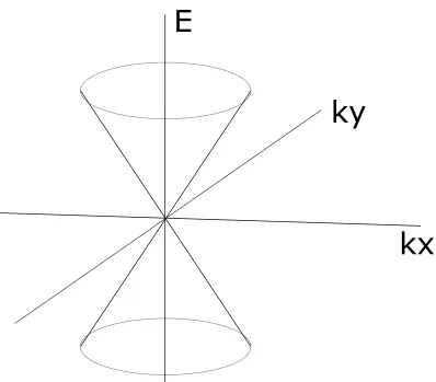
ky
E
Figure 1.1: The Dirac Cone of graphene by the K point has linear dispersion.
photocatalysis [9], capacitors [10, 11], solar cells [12], batteries [13], and sensors [14]. Properties that have been explored include geometry [15, 16, 17], mechanics [18], thermal transport [19], doping [20], and defects [21].
Structurally, graphene is a hexagonal monolayer of carbon atoms. The carbon atoms have an sp2 hybridization, leaving the final electron free to make a high mobility
π and π∗ bond. This causes the electrons to act as a 2D electron gas, as they are
confined in the out-of-plane direction but are free to propagate in plane. It is an excellent conductor of heat and is thermodynamically stable in air. It has excellent mechanical strength in-plane. It can be made through mechanical exfoliation from graphite or by growth in a furnace by chemical vapor deposition (CVD).
Electrical properties of graphene
About the K-points, graphene has a linear dispersion relation given [22]
Esk = sv|k|. (1.5)
In this equation, E is energy, k is the wavevector,s = ±1 for the valence (+1) and conduction (-1) bands, and v the Fermi velocity, 106 m/s. The effective electron mass relates to the curvature of the dispersion relation, so with a straight dispersion, the electron mass effectively goes to zero, leading to a "relativistic" effective mass mc = Ef/γ2, where gamma is a band parameter close to the Fermi velocity. Due to
the extremely low effective mass, graphene has excellent conductivity. Conductivity relates to the mobility of the graphene through
σ =e(nµe+ pµh). (1.6)
Here, σ is conductivity, e is the electron charge, n is the density of holes, p is the density of electrons, mue is the mobility of electrons, and muh is the mobility of holes. The mobility depends on the graphene scattering time. Scattering time depends on the quality of graphene. Practical values on graphene mobility can range from 2,000 cmV s2 for CVD graphene to 200,000 cmV s2 or even 1,000,000 cmV s2 for exfoliated graphene [23, 24].
Electrostatic doping of graphene
The Fermi level is the level at which at which the probability of occupation by an electron is 50%, as dictated by the Fermi-Dirac distribution. At low temperatures, this is the edge where the graphene goes from being filled with electrons to having no electrons. By apply a voltage between the graphene and gate, the graphene can be charged with either electrons or holes. The number of carriers in the graphene sets the Fermi level of the material. Ef ∝ n1/2. At the Dirac peak of the resistance, the Fermi level is zero and is known as the charge neutral point. It contains zero carrier density and is the point at which the Fermi level is aligned between the valence and conduction band.
Optical properties of graphene
In the limit of zero temperature and no doping [25],
σ =πe2/(
2h). (1.7)
Graphene absorption is due to intraband and interband effects. Intraband absorption is when the charge carriers are moved within the same band. These are lower energy behaviors and dominate in the infrared. These interband absorptions are due to the Drude-Boltzmann conductivity. The local Drude model describes the conductivity
σ as a function of frequency andEf [24]:
σ(ω,Ef)=
ie2|E
f|
π~2(ω+i/τ). (1.8)
Interband absorption occurs at higher energy effect as electrons need to be excited from the conduction to valance band. As the graphene is doped, the valence band is filled. This filling of available states Paul blocks interband transitions. This interband Pauli blocking occurs forω <2Ef, whereωis the angular frequency and Ef is the Fermi level of the graphene.
The optical surface conductivity can be calculated from the Kubo formula [26]:
σ(ω, µc,Γ,T)= je
2(ω− j
2Γ)
π~2
1
(ω− j2Γ)2 ∫ ∞
0
∂fd() ∂ −
∂fd(−) ∂ d − ∫ ∞ 0
fd(−) − fd() (ω− j2Γ)2−4(/~)2
d
,
where~is the reduced Plank’s constant, fdis the Fermi-Dirac distribution.
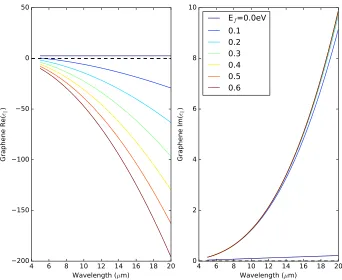
From this surface conductivity, we can calculate the permittivity of graphene [see Fig. 1.2a].
||(ω, µc,Γ,T)=r +i
σ(ω, µc,Γ,T)
0ω∆ , (1.9)
wherer is the background relative permittivity and ∆is the sheet thickness. The permittivity of graphene is dependent on the doping level
Surface plasmon polaritons, hereafter referred to as plasmons, occur at the interface of a metal and a dielectric. We do not discuss bulk plasmons in this work. Plasmons are a collective oscillation that consists of both light propagating in a dielectric and a coherent oscillation of electrons in the metal. For graphene, these excitations are typically at infrared frequencies and are dependent on the Fermi level of the material [25].
ω0 ∝ E1f/2∝n1/4
0 , (1.10)
whereω0is the plasma frequency of the graphene. Then1 /4
of the carrier concentra-tion deviates from that of the usualn1/2for other 2D electron gases[22]. Graphene plasmons sharply confine light. The confinement of graphene, λ0/λp, can reach
4 6 8 10 12 14 16 18 20 Wavelength (µm)
200 150 100 50 0 50 Gr ap he ne R e( ²|| )
4 6 8 10 12 14 16 18 20 Wavelength (µm)
0 2 4 6 8 10 Gr ap he ne Im ( ²|| )
E
f=0.0eV
[image:21.612.126.468.96.376.2]0.1
0.2
0.3
0.4
0.5
0.6
Figure 1.2: The permittivity of the in-plane compeonents of graphene. As the material is doped, the Re() goes negative as the graphene acts as a metal. This negative Re() enables graphene’s plasmonic behavior.
Spontaneous emission
The control of the spontaneous emission rate of near-field dipole is dependent on the local field of the emitter. Fermi’s Golden Rule states [27]
Γf i = 2
π ~
hf,1k|Hint|i,0ki
2
ρ(~ωk), (1.11)
whereHint = µ·Eis the interaction Hamiltonian between a dipole and the electric field, ρ is the photonic density of states, andωk = ωf i. It shows the decay of the state |i,0ki into the hf,1k| at a rate ofγf i. In case of plasmonics, the interaction of the electric field is greatly enhanced as light is confined to extremely small mode volumes. Additionally, the local density of states is enhanced. These factors contribute to a high Purcell enhancement[28]
FP =(3λ3
0Q)/(4π 2n3V),
(1.12)
where the resonant wavelength is λ = λ0/n, Q is the quality factor, and V is the
design, as the greater the Purcell enhancement, the greater the coupling between a cavity and an emitter. In the case of graphene, the low mode volume gives FP on the order of 106∼ 107for graphene ribbons [29].
1.3 Hyperbolic metmaterials
Metamaterials
Metamaterials are materials composed of subwavelength elements that together make up an effective material. By changing the behavior of these subwavelength elements, one can choose the properties of the material. There are many techniques to describe the effective index of the metamaterial, such as the Maxwell Garnett approximation or effective medium theory. They allow the creation of new effective materials that would be difficult or impossible to find in normal materials.
Metamaterials have broad applications due to their flexibility. As they can use a variety of materials, permittiviity and permeability can be engineered based on the thickness of layers for 1D metmaterials, or for arbitrary structures with 3D metamaterials. They have been used for graded index materials [30], cloaking [31, 32], negative index materials, photon-induced transparency [33], and transformation optics [34].
Hyperbolicity
The inquiry into hyperbolic materials began with Veselago’s concept of a material with a negative refractive index [35]. Hyperbolic materials consist of materials with
of different signs with the following dispersion relation:
k2
x+k2y
e + k2
z
o =
ω2
c2. (1.13)
Hyperbolic materials have many uses[38, 39], including nano-imaging, subdiffrac-tion lithography, hyperlensing, nanosensing, fluorescence engineering, and control of thermal emission [40]. They allow for broadband enhancement of spontaneous emission rates.
1.4 The Scope of this thesis
This thesis explores electrically-gated graphene in controlling light emission and propagation.
Chapter 2 focuses on the simulation of graphene nanoribbons near Er3+ emitters. By electrostatically tuning the graphene carrier concentration, we can change the response of near-field erbium atoms. By modeling Er3+ as the three level sys-tem strongly coupled to plasmons, we can explore the population dynamics and luminescence.
Chapter 3 focuses on the fabrication, measurement, and theory of a graphene/SiO2
-based metamaterial stack. By tuning the graphene, we can change in the ordinary and extraordinary response of the material. By changing the behavior at the epsilon-near-zero point, we can obtain hyperbolic dispersion by having permittivities of opposite signs.
C h a p t e r 2
ERBIUM LOCAL DENSITY OF STATES MODIFICATION BY
GRAPHENE
We propose and theoretically demonstrate electrically tunable photoluminescence from erbium ions (Er3+) coupled to graphene nanoribbons. Through electrostatic tuning of the graphene plasmon, we control the lifetimes of the upper4I11/2↔4I13/2
and lower 4I13/2 ↔4I15/2 transitions. We show a 28-fold enhancement of doped
graphene luminence at 1535 nm relative to the undoped case. We can tunably induce population inversion on the transition 4I13/2 ↔4I15/2, leading to an overall
increase of luminescence by 80% at 1535 nm.
2.1 Introduction
Surface plasmons polaritons (plasmons), the near-field collective oscillation of elec-tron density coupled to electromagnetic waves[41], have generated significant inter-est due to their subwavelength confinement of light and enhancement of spontaneous emission for field resonant particles[42]. [43, 44, 45]. In the presence of a near-field plasmonic cavity, an emitter will preferentially emit into the cavity rather free space due to the high Purcell enhancement of the cavity[46]. Graphene, a known tunable plasmonic material, has been used to modulate spontaneous emission [47, 48]. Plasmonic ribbons can quench florescence [49, 50] and have significant prop-agation losses [51]. These losses pose a significant challenge, and to overcome it various techniques have been applied, often involving introducing a gain medium [52, 53, 54, 55, 56]. As the losses directly relates to the confinement and field enhancement[57], they are a necessary component of strong field enhancement.
Ω
0γ
32(E
f(V),d)
3
2
1
Plasmon Mode 2
Plasmon Mode 1
γ
21(E
f(V),d)
PL 4
I
11/2
4
I
13/24
I
15/2d
γ
31
(a)
(b)
[image:25.612.112.504.68.220.2]V
Figure 2.1: (a) An Er3+ ion in Y2O3 is excited by a 980 nm laser at distance d
to a 8 nm wide graphene nanoribbon. It emits at 2.74 µm for the 4I11/2→4I13/2
transition and 1535 nm for the4I13/2→4I15/2transition. (b) The three-level system
of the Er3+ couples to two graphene plasmons. The Er3+ is pumped at Ω0. The
2.74 µm transition occurs at rateγ32and depends on the graphene Fermi level and
the distance between the emitter and the graphene ribbon. The 1.535µm transition occurs at rateγ32.
2.2 System Overview: Graphene Ribbons on on Er3+:Y 2O3
Our system is a graphene nanoribbon on top of a Er3+:Y2O3 [see Fig. 2.1a].
Er3+:Y2O3 is a known laser material [61, 62]. We treat Er3++ as a three-level
system [see Fig. 2.1b]. The4I15/2is the ground state |1i, the4I13/2the middle state
|2i, and the4I
11/2the top state|3i. The Er3+is pumped at 980 nm. It spontaneously
emits at 2.74(1.535) µm with a lifetime of 4.2ms(8.8ms) in the case of no graphene [63, 64].
An 8 nm graphene ribbon is electrostatically doped via a silicon backgate [see Fig. 2.1a], allowing us to tune the Fermi level of the graphene. The ribbon acts as Fabry-Perot resonator [65]. We use an FDTD simulation to find the behavior of the structure, representing the Er3+ emission with a dipole source. The dipole is located 1 nm from the edge of the ribbon and a distance d normal to the plane of the graphene. It excites a high electric field in the surrounding area [see Fig. 2.2] as it couples to the plasmonic modes of the ribbon.
at 1535 nm.
The plasmonic coupling changes the local density of of states and enhances the electric field, leading to a Purcell enhancment of the spontaneous emission rate according to Fermi’s Golden Rule. In order to calculate this change, we used the Green’s function approach, allowing us to calculate the spontaneous emission rateγ from the imaginary part of the Green’s functionGat the location of the dipole [66].
γ = πω0
3~0
|p|2ρ
p(r0, ω0) (2.1)
ρp(r0, ω0)= 6
ω0 πc2
np·Im ←→
G(r0,r0;ω0)
· np
. (2.2)
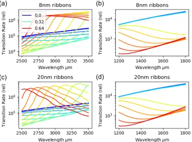
This change in spontaneous emission rate is affected by the Fermi level of the graphene [see Fig. 2.3]. At 12 nm distance, as we raise the transition Fermi level, there is a decrease in relative transmission rate at 1535 nm. In contrast, for the 2.74
µm, we see a definite decrease at for Ef=0.32 eV and Ef=0.48 eV, then a subsequent
increase for Ef=0.64 eV. This shows that close to the plasmon resonance, there’s a suppression of the spontaneous emission rate relative to the completely off-resonance case. On resonance, there is a significant increase in transition rate.
We have modeled our three-level gain medium (Er3+) interacting with the graphene nanoribbon plasmon fields on the transitions |2i ↔ |1i and |3i ↔ |2i using the Liouville-von Neumann equation [67]
Û %= −i
~
[H, ρ(i)] − L%(j), (2.3)
whereL is the Lindblad superoperator which quantifies the dissipative part of the master equation, the superscript j denotes the jt h gain medium Er3+ ion. The interaction HamiltonianH, in rotating wave approximation, can be written as
H = ~ (
Õ
j
−∆(j)
1 |1ih1|+∆ (j)
2 |3ih3| −
Ω(j)
1 |2ih1| +Ω (j)
2 |3ih2|+Ω0|3ih1|+H.c
)
.
(2.4)
Here the detunings∆1,2 = ω1,2−ν1,2whereω1,2 is the atomic transition frequency
2500 2750 3000 3250 3500
Wavelength ( m)
0
500
1000
1500
2000
2500
Relative Transition Rate
E
f=0eV
0.16
0.32
0.48
0.64
1200
1400
1600
1800
Wavelength ( m)
0
10
20
30
40
[image:28.612.116.494.79.356.2]Relative Transition Rate
Figure 2.3: The relative transition rates for two different on-resonance ribbons widths for a dipole 12 nm from a 8 nm graphene ribbon. By modulating the Fermi level, we can control the transition rate at 2.74µm as well as at 1535 nm. The black dashed lines indicate the transitions of the Er3+:Y2O3. The transition rate is relative
to that of a dipole not next to graphene.
the jt h gain medium Erbium ion is given by the coupled partial differential equation as follows:
Û
%11= γ21%22+γ31%33+i Ω∗
0%31−Ω0% ∗ 31
+i Ω∗
1%21−Ω1% ∗ 21
,
(2.5)
Û
%33 =(γ31+γ32)%33−i Ω∗
0%31−Ω0% ∗ 31
−i Ω∗
2%32−Ω2% ∗ 32
,
(2.6)
Û
%21= −(Γ21+i∆1)%21−iΩ1(%22− %11)+iΩ∗
2%31−iΩ0% ∗
32, (2.7)
Û
%31= −(Γ31+i∆1+i∆2)%31−iΩ0(%33− %11) −iΩ1%32+iΩ2%21, (2.8)
Û
%32 = −(Γ32+i∆2)%32−iΩ2(%33− %22) −iΩ∗
1%31+i∗Ω0% ∗
21, (2.9)
%11+ %22+ %33 =1, (2.10)
where the relaxation rates areΓ21 = 12γ21+γph,Γ31 = 12(γ31+γ32)+γph+i(∆2+∆1),
andΓ32 = 12(γ31+γ21+γ32)+γph. The Rabi frequency is defined asΩ1= E1℘21/2~
(a)
(b)
[image:29.612.114.497.75.358.2](c)
(d)
Figure 2.4: The radiative emission rate of a dipole position 1 nm above the metam-terial relative to a dipole with no graphene. The graphene Fermi level is varied to tune the relative couple of (a,b) 8 nm ribbons and (c,d) 20 nm graphene rib-bons. (a,c) Plasmons near the4I11/2 →4 I13/2transition. (b,d) Plasmons near the 4I
13/2→4 I15/2transition.
transitions|2i ↔ |1iand|3i ↔ |2i. Here,γi jare the decay rates for populations and
γphis the phase relaxation (or dephasing) rate of the coherence %i j due to coupling
with phonons, surface defects, etc.[68]. The emission of plasmons is described by the coherent polarization of the gain medium corresponding to the transition
|2i → |1iand |3i → |2i respectively. The corresponding time evolution equation
is obtained using the Heisenberg equation of motion for the amplitudes a1,2 and
adding the SP relaxation rateγ1,2 respectively. Here |a1,2|2 quantifies the number
of plasmon generated by the emission on transitions |2i ↔ |1i and |3i ↔ |2i. It has a similar form to the equation for the two-level gain medium, since the same transition is coupled to the plasmon field:
Û
a1 =−Γ1a1+iÕ j
%(j) 21Ω˜
(j)
5 10 15 Er3 +Height (nm)
0.0 0.2 0.4 0.6 0.8 1.0 Po p ul a tio n(
4I13/
2
)
5 10 15
Er3 + Height (nm)
0.0 0.2 0.4 0.6 0.8 1.0 Po p ul a tio n(
4I13/
2 ) P=0.01W 0.06 0.12 0.18 0.24 0.3
5 10 15
Er3 +Height (nm)
0 5 10 15 20 25 30 PL Enha nc e me nt
[image:30.612.120.495.69.321.2](a)
(b)
(c)
Figure 2.5: The population of the 4I13/2 level is dependent on distance and the
graphene Fermi level. The PL enhancement is the ratio of the graphene at Ef=0.64 eV to Ef=0.0 eV. By optimizing the distance to 12 nm, we can attain a high PL enhancement of 28 with pump powers under 10mW.
Û
a2 =−Γ2a2+iÕ j
%(j) 32Ω˜
(j)
2 , (2.12)
where Γ1 = γ1 +i∆n, Ω˜ (p)
1 = E1℘21/2~ = Ω (p)
1 /a1 similarly ˜Ω (p)
2 = E2℘32/2~ =
Ω(p)
2 /a2is a single plasmon Rabi frequency.
2.3 Results and discussion: Enhancement of Luminescence
From the rate equations, we can compute the overall occupation of the luminescent
4I
13/2 →4 I15/2 transition based on distance, pump power, and Fermi level. We
0.00 0.05 0.10 0.15 0.20 0.25 0.30 Input Power(W)
0.00 0.25 0.50 0.75 1.00 1.25 1.50 1.75
Re
la
tive
Lum
ine
sc
e
nc
e
PL change: Erbium Emission Ef = 0eV
[image:31.612.118.496.91.358.2]Ef = 0.32eV Ef = 0.64eV
Figure 2.6: Steady-state luminescence Er3+ ions coupled to on and off resonance graphene nanoribbons relative to Er3+ emission with no graphene. Doping greatly increases the luminescence of Er3+ relative from the Ef=0 to Ef=0.64 eV. Above 50mW, we show an overall increase in luminescence for heavily doped graphene. Beyond 300mW, we hit the optical damage threshold[69]
steady increase of the PL(Ef=0 eV) with distance. This maximum luminescence modulation depth of 14dB occurs occurs at 12 nm.
If we look at a fixed distance across different input powers and Fermi levels, as in Fig. 2.5, we can see a clear increase in luminescence with applied bias. With over 5mW of power, we see an increase in relative luminescence compared to the emission without graphene. By applying a graphene gate, we can induce population inversion in Er3+. The upper transition is enhanced by orders of magnitude whereas the lower transition has near unity enhancement, so the 4I13/2state becomes more heavily occupied. Whereas in the no-graphene case, the lifetime of the levels were roughly equal, with graphene we can introduce a huge enhancement to the upper transition while only slightly perturbing the lower transition rate.
10
510
410
310
210
1Time(s)
0.0
0.2
0.4
0.6
0.8
1.0
Po
pu
lat
ion
(
4
I
13/2
)
[image:32.612.122.471.102.364.2]No Graphene
Ef=0eV
0.64
Figure 2.7: Graphene nanoribbons more rapidly enhance the luminescence as they fill the 4I13/2 state sooner than normal erbium. We assume an incident power of
0.3W.
no graphene case. As we enhance the speed of various transition rates, the system should attain steady state more quickly. If the dipole were closer to the erbium, we would see an even quicker rise time, but the overall luminescence would decrease.
2.4 Conclusions
luminescence compared to erbium without graphene. Additionally, this inversion is electrostatically tunable, and can be turned on and suppressed with electrostatic doping of graphene. This effect occurs an order of magnitude more quickly than transitions in uncoupled Er3+.
C h a p t e r 3
EXPERIMENTAL DEMONSTRATION OF TUNABLE
GRAPHENE HYPERBOLIC METAMATERIAL
Previous theoretical work has suggested that actively tunable graphene elements can enable the tuning of the dielectric permittivity of metamaterials through the permittivity near zero (ENZ) regime at infrared wavelengths to yield transition from an elliptical to hyperbolic dispersion. Here, we experimentally realize and measure the response of a graphene/polar dielectric metamaterial using a graphene-SiO2 unit cell. This metamaterial exhibits epsilon-near-zero crossing and tunable
electric properties from Ef=0 to Ef=0.5 eV that are experimentally verified through spectroscopic ellipsometry and transmission measurements.
3.1 Introduction
Metamaterials are artificial composite materials with subwavelength elements that exhibit electromagnetic responses unseen in the natural world. Research in the field has been mainly driven by the desire to tailor the optical response of materials[70, 71, 36]. Particularly interesting is the case of a permittivity () near zero (ENZ) [72, 73, 74], for which one can design materials with a high photonic density of states such as hyperbolic or indefinite metamaterials (HMMs). These are typically composed as uniaxial metamaterials whose ordinary, in-plane (o) and extraordinary, out-of-plane (e) electrical permittivities have opposite signs.
k2
x+k2y
e + k2
z
o =
ω2
c2. (3.1)
This peculiar dielectric response creates a hyperbolic dispersion relation, allowing for open isofrequency surfaces and a continuum of wavevectors extending to large values for a given energy. Owing to these novel optical properties, hyperbolic metamaterials can exhibit large Purcell factor enhancements and can serve as slow-light media [75], enhance dipole-dipole interactions[76], and increase gain in lasing [55], as well as enable super-resolution [77] or sub-diffraction imaging [78].
dielectric properties of graphene can be dynamically tuned by chemical or electro-static modulation of the carrier concentration [82], allowing the design of graphene-dielectric layered metamaterials [83, 84, 85]. Additionally, it has been shown theoretically and experimentally that the plasmonic nature of graphene supports surface electromagnetic waves with extreme confinement [22, 29]. This field lo-calization, together with the tunability of graphene, provides a promising platform for investigating tunable graphene-based HMMs. There has been considerable the-oretic effort in the past decade to understand the properties of tunable graphene metamaterials. [86, 87, 88, 89, 85, 90, 84, 91]. Graphene-based HMMs can further enhance the already strong field localization of graphene plasmons due to the op-posing signs of dielectric permittivity along the different coordinate axes. Graphene heterostructures have been proposed for applications including thermophotovoltaics [92], tunable absorbers [86], thermal and terahertz emission [93, 84], device appli-cations [94], photonic logic switches [95], and elliptic-hyperbolic transitions [85]. Experimental demonstrations of graphene metamaterials utilized chemically doped graphene in order to fix metmaterial behavior [96].
3.2 Fabrication Challenges
While graphene metamaterials have been widely explored in theoretical work, fab-rication challenges have hampered experimental realization of promising struc-tures. As a two-dimensional material with weak out-of-plane Van der Waals forces, graphene exhibits poor adhesion to most dielectric substrates. Moreover, it has been challenging to fabricate methods for dielectric over-layers on graphene that are sufficiently large in area to enable metamaterial characterization and which also avoid oxidization or other damage to the graphene structure. We overcome these challenges and experimentally demonstrate a planar graphene-SiO2 metamaterial,
which is electrically gate-tunable with an external bias. A thin Al2O3 layer
en-capsulates the graphene and enables adhesion of the top SiO2to realize symmetric
Ω
+
-Figure 3.1: Left: Schematic of a theoretical metamaterial stack. Right: Schematic of the fabricated individual device. The layers: Lightly-doped silicon substrate, thermally-grown SiO2, atomic layer deposited (ALD) Al2O3, transferred
chemical-vapor deposited (CVD) graphene, electron-beam echemical-vaporated Al, ALD Al2O3, and
plasma-enhance chemical vapor deposition SiO2. The thin layers of Al2O3 are
necessary for feasibility fabrication. The thick SiO2 contribute to the majority of
the dielectric response. Contacts are added to gate and measure the resistance of the graphene. The graphene is tuned by gating against the back silicon substrate.
3.3 SiO2/Al2O3/Graphene Heterostructure
We consider a metamaterial where monolayer graphene is sandwiched between two polar dielectric materials as depicted in Fig. 3.1. Observations show an near-zero response between the polar dielectric resonances of the dielectric, in contrast to previous proposals which assumed non-dispersive materials between graphene sheets [83]. The dielectric material has two phonons, and the real part of spans from positive to negative values, therefore crossing zero. By electrostatically tuning the graphene carrier density and permitittivity, we can shift the point at which the real part of the in-plane permittivity (Re(o)) crosses zero. Since the graphene response is uniaxial, we can shift the Re(o) while leaving the extraordinary ENZ point unchanged.
[image:36.612.108.498.70.335.2]10 15 20 25 30 35
Wavelength (µm)
10 15 20 25 30 35
Wavelength (µm)
0eV 0.3eV 0.5eV SiO2 Top SiO2 Bottom
18 19 20 21 22
Wavelength (µm)
( b)
( a)
( c)
Re(
ε
o)
Re(
ε
o)
Im(
ε
o)
0 5 10
-5 0 5 10
[image:37.612.147.462.167.540.2]-2 0 2
Figure 3.2: Material parameter retrieval is used on the elllipsometric data for SiO2
and graphene to calculate effective o that is tuned with an electrical bias over a range of Fermi levels from 0 to 0.5 eV. (a) Imaginary value ofofor the SiO2and
and thus should largely affect o. Out of plane, the graphene has a constant o. The effective permittivity of the homogenized structure should consist of a tunable Re(o) that crosses zero at a range of wavelengths for different Fermi level values and a static out-of-plane permittivity (e) that crosses zero at a fixed wavelength.
The metamaterial has been designed to function experimentally with a tunable with the desired performance. The substrate is a lightly-doped silicon wafer, with a 300 nm thick layer of thermal oxide. On top of that oxide, we deposit 12.9 nm of Al2O3 by atomic layer deposition (ALD). CVD-grown graphene is transferred
onto the stack. A 0.5 nm aluminum layer is deposited on top of the graphene by electron-beam evaporation and oxidizes in ambient conditions. Another layer of 12.3 nm Al2O3 is deposited on top of the stack. The final layer is deposited
by plasma-enhanced chemical vapor deposition (PECVD) and consists of 321 nm of SiO2. Lithographically-defined patterns were used to deposit 3 nm/100 nm of
Cr/Au contacts on the graphene layer. These contacts were used to gate the graphene against the silicon backgate. This allows for the electrical tuning of the effective
o of the metamaterial. The effective Fermi level was calculated using a capacitor
model based on the materials between the gate and the applied voltage[97].
Ef =0.031 p
V−VDir ac. (3.2)
The location of the Dirac peak was experimentally determined using a capacitor model and the measured change in resistance. The thickness of the film layers was measured by both a thin film analyzer and visible ellipsometry with a qualitative agreement of roughly 2 nm.
The previous absence of experimental demonstrations of graphene/dielectric tunable hyperbolic response can be attributed to several factors: first, large-area graphene sheets on the order of mm2’s with gate-induced tunability are needed to perform metamaterial optical measurements. Exfoliated flakes are generally limited to sizes of 10s of µm, so large-area graphene samples grown by chemical vapor deposition and subsequently transferred from their growth substrates are necessary. Second, deposition of large-area thin dielectric layers on graphene is challenging. Films prepared by electron-beam evaporation exhibit thermal stress-induced delamination [98]. . Films grown by atomic layer deposition (ALD) with an H2O precursors
0.985 0.995 1.000
0.990
0.98 1.00 1.01
0.99
0.96 0.98
0.96
0.98
Theory
Experiment
(a)
(b)
(c)
Wavelength (
μ
m)
16 18 20 22 24
16 18 20 22 24
Wavelength (
μ
m)
Wavelength (
μ
m)
16 18 20 22 24
0.15 0.20 0.25
T(abs)
T(re
l)
T(re
l)
[image:39.612.146.470.102.599.2]0.6eV 0eV 0.6eV 0eV 0.6eV 0eV
deposition of trimethylaluminium (TMA) [100] or an aluminum nucleation layer [101] to create a seed layer for additional deposition. A suitably thin layer of alu-minum is needed so that it can fully oxidize and not compromise the electrical gating of the graphene. In order to create a symmetric metamaterial unit cell, ALD AL2O3layers need to be deposited. We found that deposition of AL2O3via
plasma-enhanced chemical vapor deposition (PECVD) resulted in reduced thermal stress and avoided delamination.
3.4 Effective permittivity via transfer matrices and parameter retrieval
Metamaterial structures comprised of alternating layers of polar dielectric mate-rials and graphene have two key characteristics. First, polar dielectric matemate-rials exhibit Reststrahlen bands of negative dielectric permittivity across the infrared range, which allow the near-zero crossing of the effective dielectric response of the heterostructure. Second, polar dielectric materials have high electrical breakdown strengths that support the high applied electric fields. They allow for high contrast in the optical response of graphene. We use the Kubo formula [102] calculate the sheet conductance σfrom the Ef of graphene. This value can be used to compute the transfer matrix for graphene [103].
←→
G = "
1 0
4πσ/c 0 #
.
15 20 25 -300 -200 -100 0 200 100 300 400
Δ
Re(
ϵ
)
✕
1
00%
Wavelength (
μ
m)
[image:41.612.154.448.93.381.2]Δ
Im(
ϵ
)
✕
10
0%
0 1 2 3 5 4 6 7 8 9 10 0.2eV-Re 0.4eV-Re 0.2eV-Im 0.4eV-ImFigure 3.4: Change of with applied bias.
3.5 FITR Measurements of tunable permittivity
Fourier-transform infrared spectroscopy (FTIR) was used to measure sample trans-mission and compare with predictions for calculated by material parameter re-trieval. By tuning the graphene, we were able to induce a change in transmission [See Fig. 3.3]. Our calculations predicted the experimentally-observed direc-tion for ENZ wavelength shift. Graphene becomes more metallic at higher carrier concentration, thereby increasing in absorption. This shift of the graphene Drude conductivity causes modulation of the effective permittivity of the metamaterial. The graphene exhibits hysteresis, which is attributed to defects induced by deposi-tion of the Al layer, which may account for the discrepancies between experiment and theory. As the graphene is tuned, the Dirac peak shifts in the direction of applied bias, causing the sample to experience a reduced Ef, giving qualitative experimental agreement with theory without fitting parameters.
By tuning, we have interesting behavior that occurs at the ENZ points near the SiO2
range of wavelengths dependent on the Fermi level of the graphene. From the 19.7
µm ENZ point to 20.0 µm, Re(o) is greater than zero for Ef=0 eV, whereas Re(e)
is negative. This implies our heterostructure should behave as Type I hyperbolic metamaterial (HMM). As the graphene Fermi level is raised to 0.2 eV, this region shrinks. Above Ef=0.2 eV, the Re(o)<0 while Re(e)>0, as expected for a type II HMM. At 0.5 eV, this phenomenon occurs in the wavelength range from 19.1 µm to 19.7 µm. This observation is consistent with an electrically tunable elliptic-to-hyperbolic transition in metamaterial dispersion for both type I and type II HMMs. For the longer wavelength crossings, the material should behave as a type I HMM for wavelengths in the range between 21.1µm and 21.6µm for Ef = 0 eV and up to 21.8 µm for Ef = 0.5 eV.
3.6 Conclusions
In summary, we have experimentally demonstrated a graphene metamaterial with tunable epsilon-near-zero permittivity response. By tuning the graphene Fermi level, we can modulate the ENZ wavelength by up to 0.9µm. Ellipsometry was used to determine the optical properties of the constituent materials. Material parameter retrieval was used to calculate the constitutive electromagnetic response. These calculations closely matched the FTIR transmission measurements of the overall heterostructure, indicating a shift of the graphene permittivity near the ENZ point under electrical gate bias. Near 19.7µm we can tune electrically tune , which implies an elliptical to hyperbolic transition in dispersion.
3.7 Methods: Fabrication
In this section, we will describe the process used to fabricate the metamaterial. The device required extensive process engineering. Of the nine different layers in the heterostructure, many methods were employed in order to find the optimal process. In addition, several other device geometries were explored. The initial conception of the project was more a simple SiO2/Graphene/SiO2. This original concept was
expanded greatly in order to make a device that was symmetric, large area, and stable in air.
The substrate was purchased from MTI. It was a 300nm thermally grown SiO2
Figure 3.5: A layer by layer depiction of the full graphene metmaterial stack, the layer thickness by two different modes of measurement, and the process used to create the layer.
Atomic layer deposition of Al2O3
Deposition of the Al2O3 was performed using a Fiji G2 Plasma Enhanced Atomic
Layer Deposition System. TMA was used as the precursor. The chamber was heated to 150°C. This layer allowed for a greater gate bias to be applied, as Al2O3 has a
high breakdown strength. Additionally, application of a thin layer of Al2O3 would
fill pin-holes in the underlying material, which are the sources of failure in graphene gate bias measurements.
Graphene Transfer
The graphene on copper with PMMA was purchased from Graphena and had a specification sheet mobility of 3,760 cmV s2. Raman measurements were used to confirm that the graphene was primarily monolayer [see Fig. 3.10a]. Graphene transfer allows the graphene to be moved from the copper to the SiO2/Si substrate.
(a)
(b)
Figure 3.6: An image of PMMA on graphene using a confocal microscope. (a) The graphene had been immersed in acetone for 45 minutes, but this did not remove all the PMMA, as shown by the orange patches. (b) The graphene with three acetone baths of 45 minutes
The remaining PMMA/graphene sheet is scooped up with a spoon and placed in a a succession of four water baths. Care must be take in order to pick up the floating sheet without having it stick to the sides. Spraying water breaks the surface tension of the water, allowing for an easier transfer. Large baths, coupled with wait times, allow the samples to be fully cleaned of iron chloride. Immediately before the transfer, the SiO2/Si substrates are cleaned in an oxygen plasma clean. This process
makes the sample more hydrophobic, allowing the graphene to more readily stick to the surface. The SiO2/Si chip is used to scoop the graphene out of the final water
bath. It is then heated overnight at 60C in order to evaporate the water that was caught between the graphene sheet and the substrate.
PMMA removal from graphene
Initially, 45 minutes in acetone was used to remove PMMA [see Fig. 3.6a]. However, this immersion did not fully remove the reside. PG remover was not a solution, as it resulted in the complete removal of the graphene.
remove significantly more PMMA than just 45 minutes in acetone[see Fig. 3.6b].
Cr/Au Contacts
Contacts are initially patterned using a Raith 5000+ direct write electron beam (e-beam) lithography system. A two layer resist is used. The first layer consists of PMMA 495A4 deposited at 3000rpm for 60 seconds and baked at 180C for 150 seconds. The second layr consists of PMMA 950A2 deposited at 3000rpm for 60 seconds and baked at 180C for 150 seconds. A two-layer resist was used in order to have a cleaner lift-off process. The lower molecular weight resist dissolves first, allowing the top to be removed. Single layer resists can stick to the sample, making it difficult to remove the metallization layer.
The contacts are deposited using a CHA Mark 40 e-beam evaporator. The conacts are 3 nm of Cr deposited at 0.5 Å/s followed by 100 nm of Au, deposited at 1.5 Å/s. These contacts are consistent with those found in literature for gating graphene devices. Once the contacts have been deposited, the e-beam resist is removed by immersing the sample in acetone for 45 minutes. It is the sprayed with acetone to remove any excess gold. It is then sprayed with isopropanol and dried with compressed nitrogen.
Aluminum deposition by electron-beam evaporation
Aluminum was deposited using a Lesker Labline e-beam evaporator. The settings were set to deposit 5 Åat 0.5 Å/s. As the deposition occurred over a relatively short amount of time and a very thin layer of aluminum was deposited, more material would be deposited than was set on the system. Measurement by thin-reflectrometry showed a layer thickness of 4.63 nm. Note that the thickness of this layer is important, as it needs to completely oxidize in air in order not to adversely affect the graphene tunability. If the system were set for 10 Å, the electrical properties of the device would be compromised.
This Al was deposited in order to serve as nucleation layer to the follow ALD steps. By adhereing metallic Al to the graphene, we can overcome the weak Van Der Waals interaction that precludes adhesion to other materials. Exposure to oxygen naturally oxidizes the Al into Al2O3in ambient conditions. By depositing a sufficiently thin
Al2O3 was used over other methods such as 3,4,9,10-perylene tetracarboxylic acid
(PTCA) functionalization [106] as it deposits a clean uniform layer. PTCA suffers similar issues to the PMMA removal from the Graphena graphene in that it leaves a non-uniform residue on the sample. As a large area of graphene is needed for the following measurements, the PTCA method was not a viable option.
Further atomic layer deposition of Al2O3
Deposition of the Al2O3 was again performed using a Fiji G2 Plasma Enhanced
Atomic Layer Deposition System. By depositing onto Al2O3rather than graphene,
the Al2O3 was able to successfully adhere to the sample. A non-ozone process
was used, as ozone would oxidize the graphene[see Fig. 3.10c]. By measuring the thickness of the underlying Al2O3layer as well as the Al layer, the number of cycles
to be run can be calculated. By reducing the number of layers, we can preserve the symmetry of the structure by ensuring an equal thickness of Al2O3above and below
the graphene.
Plasma-enhanced chemical vapor deposition of SiO2
An Oxford PECVD deposits a layer of SiO2 on the sample. As PECVD is not a
precise process between runs occuring at different times, a number of calibration runs were needed in order to deposit with precision. A PECVD flows gas into a chamber, which then will react and deposit material. Rather than a self-passivating ALD, PECVD deposition rate is dependent on the gas flow over the surface of the chip. Therefore, the deposition is non-uniform, with the edges of the chip receiving less SiO2. This non-uniformity imposes the condition on the experimental design
that the chip needs to be sufficiently large that the deposition on the graphene is uniform. By placing a Si chip on the contacts, they can be shielded from the SiO2,
which is necessary for the subsequent wire bonding. This requirement also imposes the condition that the contact pads need to be sufficiently long. A shielding Si chip is placed sufficiently far away, typically a few mm’s, such that the deposition on the graphene remains relatively uniform.
The reason PECVD was selected over other methods to deposit the top SiO2is that
Figure 3.7: Top SiO2delaminates from samples when deposited by e-beam
evapo-ration. There is high thermal stress in a film deposited by e-beam evapoevapo-ration. As the film cools, it causes stress in the film. The effects are visible to the naked eye. Graphene is the pale purple region and occupies most of the area save for the far left region. The blue wave lines are the delatminated regions. The delaminated region coveres nearly the entire sheet of graphene. Delamination begins at a single point and spreads across the sample. It can occur a number of minutes after the device has left the e-beam chamber. If the device is left in the e-beam chamber in vacuum to slowly cool overnight, it will still delaminate.
processes, PECVD caused the least thermal stress, leading to it being chosen to deposit the top SiO2.
Wire Bonding to the contacts
Different amounts of energy needed to be used for different wire bonding steps. A low current was needed for bonding to the gold pads on the ceramic chip. Lower energies were used to bond to the sample itself. The field needed to be sufficient to go through the 12 nm of Al2O3 and bond to the gold without punching through
the material and shorting to the underlying Si. In bonding to the Si directly for the backgate, high fields were used as it is difficult to directly bond gold to Si.
Electrical bias
Electrical biases were applied between the top gold contact and the underlying silicon backgate. The electrical resistance was read using a multimeter between two of the gold contact pads. A bias was applied using a Keithley Sourcemeter.
The quality of the gate was monitored by recording the leakage current through the SiO2. With little to no bias, the leakage current was under 1 nA [see Fig. 3.8]. As the current was applied. At high voltage levels, a successful gate had under 1µA of current. For samples whose gate failed, the leakage current exceeded 10µA under 2V of bias. If a sample was over-biased, it would fail catastrophically and destroy the sample. The silicon would short to the graphene and high charge would flow across the short. Even after the voltage was reduced, this short would still exist, making the sample unsuitable for gating.
3.8 Methods: Sample Characterization
Thickness
50
0
50
100
150
Voltage (V)
0
1
2
3
4
5
6
7
[image:49.612.134.466.103.366.2]Leakage Current (nA)
Figure 3.8: A representative response of a sample under going electrical bias. Most samples were tested between -150V and 150V as they were liable to fail much beyond those voltage. There is a sharp increase in the leakage current under high bias.
Electrical Measurements
Electrical measurements are used to determine the Fermi level of graphene. Initial measurements showed the Dirac Peak occurred at high bias voltages. [see Fig. 3.9a]. However, once a metalization layer of aluminum was deposited on the graphene, there was a large shift in the Fermi level [see Fig. 3.9b]. This effect is theorized to occur due to charge trapping in the graphene. The aluminum oxidizes to Al2O3,
causing a shift in the Fermi level. There is also a large hysteresis, and when a voltage is applied, the graphene resistance will slowly change with time.
Raman Measurements
(a)
[image:50.612.106.491.75.390.2](b)
Figure 3.9: (a) Applied bias versus graphene resistance after the graphene was transferred but before ALD. Note that the maximum resistance, the Dirac Peak, is at 180V. (b) Applied bias versus graphene resistance after aluminum metalization. The Dirac peak changes, from -60 V to 0 V due to hysteresis.The two lines represent the resistance measurement that was achieved immediately once hitting the voltage and after a minute of dwell time. Measurements were taken by moving 5 V once a minute and having a 5 minute dwell time at the maximum and minimum voltages.
nucleation layer on top of the graphene successfully protects it from the additional ALD deposition and PECVD. Had it been oxidized, it would have the additional graphene oxide peak as seen in Fig. 3.10c.
FTIR measurements
(a)
(b)
Raman Shift (cm-1)Raman Shift (cm-1) Raman Shift (cm-1)
Numbe
r Count
Numbe
r Count
(c)
Number Count
Oxide Peak
[image:51.612.106.506.146.584.2]Raman Shift (cm-1) Raman Shift (cm-1)
The measurements were conducted in the main chamber of the FTIR. An adjacent microscope provided the source, but due to the detector configuration, the measure-ments had to be done in the main chamber with no aligning optics. Therefore, a metal disk with a hole in it was used to select the area of the sample of measurement. The hole was a few mm in diameter. In order to conduct these experiments, it was necessary to visually align the whole with the area of graphene or reference sample. Large area samples of graphene, up to 8 mm by 10 mm, were used in order for this technique to only hit the sample.
In order to calibrate the measurements, a variety of reference measurements were made. Each detector and beam splitter configuration needed separate backgrounds. Additionally, backgrounds taken against the metamaterial without graphene were taken as well. In the post-processing of the data, the sample data was divided by the reference background in order to calculate transmission.
There were a number of sources of noise in the measurement. The sample itself changes the optics of the measurement. As light needs to be transmitted through the thick SiO2and underlying silicon in order to reach the detector, it will slightly
change the focus of the FTIR. Therefore the ratio of the sample measurements to the reference measurements without the sample were not an absolute measurement. Water vapor contributes noise in the infrared, as water has a number of strong absorption lines. The chamber had a vent system that would gradually purge the water and fill the chamber with nitrogen, reducing the noise from the water vapor. An additional source of noise is detector drift. Over the course of minutes and hours, the detector response will slowly drift. This drift sets a limit on the accuracy of the measurement. By increasing the length of the measurement sampling, the noise drops as the
√
n, where n is the sampling time.
IR Ellipsometry
block unwanted reflections.
A set of reference samples were used. By using a reference sample, we could confirm the properties of the substrate, check thickness, and have a basis for the final model. The reference samples that were used were bare silicon, Si with 150 cycles of ALD Al2O3, Si with 150 cycles of ALD Al2O3, and PECVD SiO2.
The underlying silicon was represented by a general oscillator. We then used a surface roughness layer of 1.36 nm thickness with a 50% fill fraction and a top native oxide layer of 1.635 nm. The thermal SiO2was fitted 295.451 nm, in close
agreement with the 300 nm thickness specification of the company we had purchased it from. We had an MSE of 2.612 for the the ellipsometric fit[see Fig. 3.11]. The bottom ALD Al2O3 layer was 12.8 nm. On top of it was a layer of graphene,
represented by a 2 nm thick general IR oscillator. The top Al to Al2O3layer was fit
as a different material than the ALD layers, as it was deposited by a different method and therefore could have different optical properties. It was 3.72 nm thick. On top of the was 11.85 nm of ALD Al2O3. Finally, the PECVD layer was 321 nm thick.
Figure 3.11: The ellipsometer fit of the ellipsometric model to the data for Si/SiO2.
We see good agreement with the data. There are clear absorption lines of the SiO2
near 8nm and 20nm due to phonos.
[image:54.612.115.498.419.662.2]