Abstract—Redundant Binary Signed Digit Adder and Multiplier circuits are logic circuits which are designed to perform high-speed arithmetic operations. Fast RBSD adder cell, proposed by Kal and Rajshekhar in 1990 was modified by Neelam Sharma in 2006 using universal logic. The proposed adder is re-modified for reducing the number of gates and thus the circuit complexity and cost. Further due to the reduced gate count, circuit area, number of levels and hence implementation time is reduced up to 1% as proved by VHDL synthesis report. Since multiplication is repetitive addition, the implementation time of the multiplier circuit will be reduced to a great extent. Thus the proposed RBSD adder cell using NOR and NAND gates will be a boost in the speed of sophisticated ALU Design of high speed machines.
Index Terms—Carry free addition, fast Multiplier, Fast Computing, High-speed arithmetic, RBSD.
I. INTRODUCTION
Addition is the basic arithmetic operation for all mathematical operations like multiplication, division, square rooting etc. With recent development in technology of integrated circuits, various high-speed circuits with regular structures and low power design have been proposed. The circuits for arithmetic operations still suffers some problems like propagation time delay, limited range of the number of bits and complexity in hardware. Redundant Binary Signed Digit (RBSD) numbers is particularly gaining much attention due to the capability of carry free addition [1], [2], [3].
The performance of circuit also depends upon the suitable hardware design. The logic gates are responsible for the high-speed arithmetic operations [4]. Therefore it is highly desirable to construct digital logic circuits using universal gates because of simplicity and uniformity in circuit. These circuits just have a single primitive component of universal gate i.e. either NOR or NAND gate. Since these gates can be manufactured quite economically, therefore they contribute to the major components used today by logic designers. The use of field programmable gate arrays (FPGA) allows the development of high performance customized hardware. Selecting suitable arithmetic algorithms and applying optimal mapping strategies for FPGA technology can develop the high performance implementations [5].
Manuscript received November 17, 2010.
Rakesh Kumar Saxena is Associate Professor in the Institute of Engg. & Technology, Alwar, Rajasthan, India (e-mail: [email protected]).
Neelam Sharma is Professor of Electronics Engineering and Principal of the Institute of Engg. & Technology, Alwar, Rajasthan, India (e-mail: [email protected]).
A. K. Wadhwani is the Professor of the Electrical Engineering in Madhav Institute of Technology & Science, Gwalior, M.P., and India. (e-mail: [email protected])
This paper emphasizes briefly about RBSD number system and RBSD adder design in the sections 2 and 3. The concept of logic design for RBSD adder cell suggested by Kal and Rajshekhar in 1990 [6] and by N. Sharma et. al. in 2006 [7] is described in the sections 4 & 5 respectively. Further in section 6 the modified architecture of adder cell using universal logic has been proposed. The comparison among the previous and proposed cell structures is given in section 7. Finally in section 8, comparison among Ripple carry adder (RCA), Carry Look Ahead adder (CLA) and RBSD adder upto 64 bit length is presented.
II. REDUNDANT SIGNED DIGIT NUMBER SYSTEM
This number system was proposed by Avizienis in 1961 [1]. RBSD numbers can be represented using the digit set (1, 0,) unlike binary number system, which is represented, with digit set (0, 1). The decimal value of RBSD number can be calculated by following relation.
(1) Let the number (4)10 can be represented in binary as 0100.
The same number in RBSD may be represented by more than one representation i.e. 100 or 100. Hence in this number system, a number can be represented by more than one way, called redundant representation. This redundant number representation proceeds to the technique for carry free addition [2].
III. ADDER DESIGN
Adder is the basic building block for the computation of all mathematical operations. Hence a carry free adder design is highly desirable when the number of bits becomes large. It can be achieved with the help of RBSD number system [9], [10], [11].
The following equations suggested by Rajshekhar and Kal, are used for the carry-free addition [6].
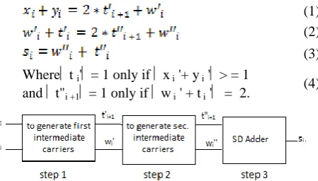
(1) (2) (3) Where t i' = 1 only if x i '+ y i ' > = 1
and t"i +1 = 1 only if w i ' + t i ' = 2.
(4)
Fig. 1. Three step RBSD Addition Process
Fast Adder Design using Redundant Binary Numbers with
Reduced Chip Complexity
The three step RBSD addition process described by equations 2-4 is shown in fig. 1 in which first and second step generates intermediate carriers (carry and sum) and third step gives the final result. The variables x i, yi are the addend and
augends in RBSD, ti' and ti" are intermediate carriers, wi' and
wi" are the intermediate sums at the ith stage, „si‟ is the final
sum. The variables ti" and wi" can never be both +1 and –1
simultaneously at second stage and hence gives carry free addition. Therefore the input numbers can be added simultaneously in parallel, as there is no rippling of carry from LSB to MSB.
IV. RBSDADDER CELL
It is known that the logic gates do not support the negative logic (-1) therefore to represent -1, 0, 1 in RBSD the binary encoded form i.e. (0, 1), (0, 0), (1, 0) is used to encode -1, 0, 1 respectively. With this idea, Kal and Rajashekhar, 1990 has given following Boolean expressions (equation 5 to 9) for RBSD addition in binary encoded form [6], [7].
di = mi xi+xi-yi+yi- (5) mi+1 = xi +yi+ (6) bi+1 = mixi+xi- + xi+yi+ + yi+yi- mi
+ xi+xi- yi+yi- (7) si+ = di bi (8) si- = di bi (9)
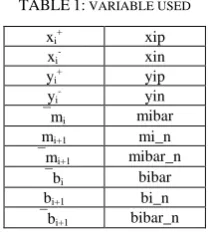
where m i ,b i and d i are binary variables and xi*, yi* are
RBSD input numbers and si* output sum in RBSD with digit
set (-1, 0, 1) represented by binary encoded form i.e. (0, 1), (0, 0), (1, 0) respectively. The binary variable representation corresponding to augends‟ (xi*), addend (yi*) and sum (si*)
are xi+ xi-, yi+ yi- and si+ si- respectively. TABLE1: VARIABLE USED
xi+ xip
xi- xin
yi+ yip
yi- yin
mi mibar
mi+1 mi_n
mi+1 mibar_n
bi bibar
bi+1 bi_n
bi+1 bibar_n
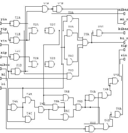
The circuit shown in fig. 2 is the RBSD adder cell implemented using equations 5-9 and suggested by Kal et.al.
This cell designed to add 1 bit RBSD number. The same circuit connected in parallel can be used to add n bit numbers. In this logic diagram, the various inputs and outputs used from the equations 5-9 which are expressed as per table 1 and are further used for the simulation of RBSD adder cell using universal logic.
V. RBSDADDER CELL USING UNIVERSAL LOGIC
In 2006, N Sharma et. al. proposed the adder cells using universal logic [7]. The logic circuit design using universal gates is highly desirable due to uniformity in the circuit. These circuits can be designed through either NOR or NAND gates as these gates are in-expensive in manufacturing aspects, therefore they are preferred by the logic designers.
Universal gates are available in SSI package that vary in size containing up to four gates per package. Keeping above aspects in mind the adder cell shown in figure 2 is redesigned using NOR-NOR logic and NAND-NAND logic as shown in figure 3 and 4 respectively.
The delay time of these adder cells found less as compared to the previous circuit suggested by Kal [7].
Fig. 2. Logic circuit of Basic RBSD adder cell
Fig. 3. RBSD Adder Cell: NOR-NOR Logic
U1A U2A
U3A
U4A
U5A
U6A
U7A U8A
U9A
U10A
U11A
U12A
U13A U14A
U15A U16A
U17A
U18A U19A
U20A U21A
U22A
U23A U24A
U25A
U26A yip
yin
xip
xin
mibar_
bi_n
sip
sin mi
bi
bibar
mi_n
Fig. 4. RBSD Adder Cell: NAND-NAND Logic.
VI. MODIFIED RBSDADDER CELL DESIGN USING
UNIVERSAL LOGIC
In this section, the modified architectures of adder cell with reduced number of (i) NOR gates and (ii) NAND gates has been proposed as compared to the design shown in figure 3 and 4.
A. Methodology to reduce the Gate count
The reduction in gate count in proposed designs is basically due to the redesign of three input XOR gate (used in fig. 2) with universal logic.
The basic logic equation for 3-input XOR gate shown in fig. 5(a) is
Y = A B C (Let A, B, C input and Y output) = (10) The above logic equation can be implemented using 4 AND and 1 OR gate as shown in figure 5(b).
This logic diagram can also be implemented using 6 NOR gates or 5 NAND gates shown in figure 5(c) and 5(d) respectively by replacing equivalent universal logic implementation of 3 input AND and 4 input OR gate used in fig. 5(b) and on applying changed inputs (i.e. A BC, AB C,
A BC, ABC) to the various 3-input NOR gates. B. Modified Adder Cell
The output di produced by 3-input XOR gate in basic
RBSD adder cell (refer fig. 2) has been achieved after 10 NOR gates (U15A to U24A) in the adder cell proposed by N Sharma using NOR-NOR logic as shown in figure 3. In other words here the 3 input XOR logic was prepared using 10 NOR gates and passing the signal over 8 logic levels. But in proposed modified design the same output can be achieved using 6 NOR gates (U5A, U11A, U15A, U16A, U18A and U19A) only and 3 logic levels as shown in fig 6. Hence the Modified adder cell has been designed using 22 NOR gates only.
Similarly the output di in NAND-NAND adder cell
proposed by N Sharma shown in fig. 4 has been achieved after 8 NAND gates (U4A, U4B, U4C, U4D, U5A, U5B,
U5C & U5D) and passing the signal over 7 logic levels. But in proposed modified design the same output can be achieved using five NAND gates (U7A, U7B, U7C, U8A & U6B) only and after 2 logic levels as shown in fig 7. One more NAND gate is reduced due to no need of signal mi_n for further stages in modified design. Hence the Modified adder cell has been designed using 26 NAND gates only.
It is clear from the figure 6 and 7 that the increased performance of these circuits in comparison to the circuit shown in fig 3 and 4 is due to decrement in the count of NOR gates and NAND gates which cause reduction in circuit area. Further the reduction in logic levels to travel the signal causes reduction in the propagation delay time to get the output.
Fig. 5. (a) 3 input XOR (b) 3 input XOR using AND & OR gates (c) using NOR gate (d) using NAND gate
Fig. 7. Modified Cell: NAND-NAND logic
VII. COMPARISON OF VARIOUS ADDER CELL
A. Hardware
Table 2 shows a clear comparison among the circuit shown in figure 3, 4, 6 and 7. It is clear that the proposed modified architectures are better due to less number of gates required, less number of input pins and signal passes less number of levels to get the final sum.
TABLE 2:COMPARATIVE ANALYSIS AMONG VARIOUS ADDER CELLS
Type of Adder Cell
NOR / NAND Gate used I/P Pins
Levels Required
for O/P 2
I/P 3 I/P
4
I/P Total si+ si
-NOR-NOR 25 -- 1 26 7 9 8
Modified
NOR-NOR 16 4 2 22 6 6 6
NAND-NAN
D 29 -- 1 30 7
1 1 10 Modified
NAND-NAN D
20 4 2 26 6 8 8
B. Simulation
All the adder cell architectures are verified using Multisim software. Further the VHDL code is also generated on Xilinx project navigator for the simulation, synthesis and the timing reports generation. These circuits are also verified on field programmable gate arrays (FPGA).
C. Time Delay
The propagation delay time reports using Xilinx Project Navigator (Software for VHDL synthesis) were generated and results obtained are shown in table 3 and in fig 8. Here it can be concluded that the delay time to get the addition result for one bit addition is less and reduced up to 1% in modified architectures as compared to previous one.
TABLE 3:TIME DELAY
RBSD Adder Cell Type
Time Delay (ns)
Percentage (%) Reduction in Time Delay
NOR-NOR 11.861 --
Modified
NOR-NOR 11.807
0.455 (Compared to NOR -NOR Logic)
NAND-NAND 11.978 --
Modified
NAND-NAND 11.861
0.9767 (Compared to NAND-NAND Logic)
Fig. 8. Time delay in different architectures of Adder cell
VIII. IMPLEMENTATION AND TIMING ANALYSIS OF RCA, CLA AND RBSDADDER
In this section the VHDL implementations of Ripple carry adder (RCA), Carry Look Ahead Adder (CLA) [12] and RBSD adder of n-bit is simulated on modelsim simulator and synthesized on xilinx project navigator and their timing reports were observed.
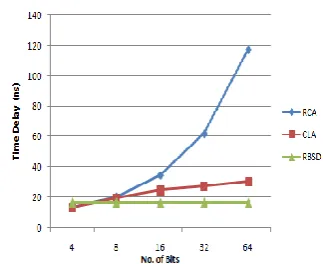
A comparative graph among RCA, CLA and RBSD adder is shown in figure 9. It is observed that the delay produced in RBSD adder is constant (16.51 ns) which is very less for any number of bit additions as compared to CLA and RCA. The addition time increases in RCA with increase in number of bits due to rippling of carry from LSB to MSB. In CLA the add time increases gradually due to logic for carry calculation and hence circuit changes with increase in bits. Hence for higher bit length, RBSD adders are suitable due to carry free addition and symmetrical circuit.
Fig. 9. Timing comparison among RCA, CLA and RBSD Adder
IX. CONCLUSIONS
improve the overall processing time of entire ALU. The number of gate counts have been reduced in the proposed adder cell from 26 to 22 in NOR-NOR and 30 to 26 in NAND-NAND logic and hence overall reduction in number of logic levels and inputs will also reduce the area and chip complexity. Therefore the proposed modified RBSD adder cell is highly appreciable for design of ALU of higher bit length.
In digital design techniques, much attention has to be paid to network design in the form of repeated pattern of identical circuits. Therefore the redundant adder has a high advantage of constant and less delay time for any number of bit additions. The CLA adders are suitable only upto 12 bit addition and thereafter addition using redundant adders is suitable for 64, 128, 256 bit adders.
The efficiency of RBSD adder increases as bit length of the summands increases. The higher the bit length, the efficiency of RBSD adder as compared to CLA will increase. Finally addition is the base for all the mathematical operations, fast arithmetic processor of higher bit length can be designed using proposed architectures of adder cell.
REFERENCES
[1] Avizienis, A., “Signed digit number representation for fast parallel arithmetic”, IRE Trans. Electron Computers., vol EC-10, pp. 389-400, sept.1961.
[2] Hwang, K., Computer Arithmetic/Principles,Architecture and Design,
New York : Wiley 1979.
[3] Parhami B, “Carry free Addition of Recorded Binary Signed-Digit Numbers”, IEEE Transactions on computers, vol. 37 no. 11, pp. 1470-1476 ,1988.
[4] Chow C. Y. and Robertson J. E. “Logical Design of a Redundant Binary Adder”, Proceedings of 4th Symposium on Computer
Arithmetic, pp. 109-115, 1978.
[5] Mak W. K. “I / O Placement for FPGAs With Multiple I/O Standards”,
IEEE Transactions on Computer Aided Design of Integrated Circuits
and System, vol. 23, no. 2, pp. 315-320, 2004.
[6] Rajashekhar, T .N. and Kal, O., “Fast Multiplier Design using Redundant Signed- Digit Numbers”, International Journal of Electronics, vol .69, no. 3, pp –359-368, 1990.
[7] Neelam Sharma, B. S. Rai and Arun Kumar, “Design of RBSD Adder and Multiplier Circuits for High Speed Arithmetic Operations and Their Timing Analysis”, Special Russian Issue: Advances in computer
Science and Engineering, Research in Computing Science23, pp.
243-25, 2006.
[8] Rajashekhar, T.N. and I-Shi Eric Chen, “A Fast Adder Design Using Signed-Digit Numbers and Ternary Logic”, Proc. IEEE Southern Tier
Technical Conference, pp.187-194, Binngamton, New York, April
1990.
[9] Cortadella J. and Lang T., “High Radix Division and Square – Root with Speculation”, IEEE Transactions on Computer, Vol. 43, No. 8, pp. 919-931, 1994.
[10] Cotolora, S. and Vassiliadis, S. “Signed Digit Addition and Related Operations with Threshold Logic”, IEEE Transaction on Computers,
vol. 49, no. 3, March 2000.
[11] M D Ercegovac, J M Muller, Tisseran., “Reciprocation, Square root, Inverse Square root and some Elementary functions using small Multipliers”, IEEE Transactions on computers, vol 49, No. 7, July 2000.
[12] Gloria A. D. and Olivieri M., “Statistical Carry Look-ahead Adders”,
IEEE Transactions on Computers, vol. 45, No. 3, pp. 340-356, 1996.
[13] Fagin B. S., “Fast addition of large numbers”, IEEE Transactions on Computers vol. 41, no. 9. pp. 1068-1077, 1992.
[14] Perry D. L., VHDL Programming by Example, Tata Mc Graw – Hill Publishing Co. Ltd. Fourth Edition 2003.
[15] Rakesh Kumar Saxena, Neelam Sharma and A. K. Wadhwani, “Fast Arithmetic using Signed Digit Numbers and Ternary Logic”
International Conference Proceedings, Institute of American Physics, USA, vol. 1146, pp 488-498 July 2009.
[16] Salivahanan S. and Arivazhagan S, Digital Circuits and Design, Vikas publishing house, 2nd edition, 2003.
Rakesh Kumar Saxena received the M. Tech from Dayalbagh Educational Institute, Faculty of Engineering, Agra, India in 1998. Currently, he is pursuing the Ph.D. in Electronics Engineering from Rajeev Gandhi Technical University, Bhopal MP, India. His research is in the area of Digital systems and Computer Architecture. Presently he is working as Associate Professor (EIC) in Institute of Engineering and Technology, Alwar, Raj. India. He is member of IEEE, International Association of Computer Science and Information Technology (IACSIT), Institution of Engineers (IE) India, Indian Society for Technical Education (ISTE), Delhi, India and Institution of Electronics and Telecommunication Engineering (IETE), Delhi, India.
Neelam Sharma received the PhD and M.Tech from U.P.T.U., Lucknow UP and B.E. from Thapar Institute of Engineering and Technology, Punjab India. Dr Sharma is a Goldmedelist of Guru Nanak Dev University, Amritsar, Punjab, India in Pre engineering examination. Presently she is Professor in the Department of Electronics and Instrumentation Engineering, Institute of Engineering and Technology, Alwar, Raj. India. Her current research interests are Computer Architecture, Neural Networks, VLSI, FPGA, etc. She has twenty five research publications and convened number of sponsored research projects. She is member of IEEE, Institution of Engineers, India, Institution of Electronics and Telecommunication Engineering, Delhi, India and Computer Society of India.