5
X
October 2017
Implementation of Reversible Control and Full
Adder Unit Using HNG Reversible Logic Gate
Naresh Chandra Agrawal1, Anil Kumar2 , A. K. Jaiswal3 1
Research scholar, 2Assistant Professor, 3Professor, 1, 2, 3
Department of Electronics & Communication Engineering, SHUATS, Allahabad, UP, India
Abstract: Reversible logic is one of the most vital subject at present time,used to reduce the power dissipation that occurs in conventinal circuits by preventing the loss of information, in this paper we are presenting the implementation of efficient arithmetic logic i.e. reversible control unit and reversible full adder unit, using reversible HNG logic gates which can performseven logical operations and eight arithmetic operations. Alsoour focus on improving the performance parameters of design: number of constant inputs, number of garbage outputs, quantum cost, number of gates and propagation delay compared to existed designs.
Keywords: Reversible logic gates, HNG gate, Control unit, Full adder, Fault,
I. INTRODUCTION
As the complexity of VLSI circuits increases, and number of transistors on integrated circuits increases rapidly hence power dissipation by these also increases. In Conventional logic circuits, every time one bit information is lost during computation hence heat is generated due to the loss of bit. In order to avoid this loss of information the Conventional circuits are designed using Reversible logic.
[image:2.612.63.550.432.679.2]is a digital circuit and it executes arithmetic and logical operations on binary numbers. It is data processing componnt in CPU. Arithmetic operations includes add, minus, increment, decrement, operations while in logical operations AND, OR, NOR and NAND, Ex-OR etc. are present. We can reduce the power dissipation if above functions can be realized by using reversible HNG gates. As we know, ALU contain control unit and adder so we need to design reversible control unit and reversible full adder. By cascading the control unit and full adder we can implement the reversible ALU. Fig 1 is the block diagram of proposed 1-bit reversible ALU design for three control signal which performs 8 arithmetic operations and 7 logical operation as mentioned in the Table 1
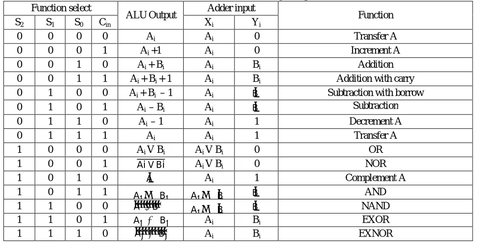
Table - 1 Arithmetic and logical operations Function select
ALU Output Adder input Function
S2 S1 S0 Cin Xi Yi
0 0 0 0 Ai Ai 0 Transfer A
0 0 0 1 Ai +1 Ai 0 Increment A
0 0 1 0 Ai + Bi Ai Bi Addition
0 0 1 1 Ai + Bi + 1 Ai Bi Addition with carry
0 1 0 0 Ai + Bi – 1 Ai Bı̇ Subtraction with borrow
0 1 0 1 Ai – Bi Ai Bı̇ Subtraction
0 1 1 0 Ai – 1 Ai 1 Decrement A
0 1 1 1 Ai Ai 1 Transfer A
1 0 0 0 Ai V Bi Ai V Bi 0 OR
1 0 0 1 Ai V Bi Ai V Bi 0 NOR
1 0 1 0 Aı̇ Ai 1 Complement A
1 0 1 1 A B A Bı̇ Bı̇ AND
1 1 0 0 Aı̇ ⋀Bı̇N A Bı̇ Bı̇ NAND
1 1 0 1 A ⨁ B Ai Bi EXOR
Fig 1 block diagram of proposed 1-bit reversible ALU design.
II. LITERATURE REVIEW
The amount of energy (heat) dissipated for every irreversible bit operation is given by 2, which is small but not negligible[1].
If we could compute entirely with reversible operations, there would be no lower limit on energy consumption. 2 energy
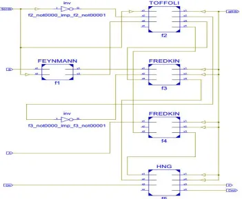
dissipation would not occur, if a computation is carried out in a reversible way [2], since the amount of energy dissipated in a system bears a direct relationship to the number of bits erased during computation. Low-power multiplexer-based 1-bit full adder that uses only 12 transistors and the new adder has more than 26% in power savings over conventional 28-transistor CMOS adder. Also, it consumes 23% less power than another 10-transistor adder and is 64% faster [3]. Low power operations [4], which can use the lowest possible supply voltage coupled with architectural, logic style, circuit and technology optimizations. A synthesis model and a synthesis procedure which allow us to minimize the number of garbage outputs [5], in reversible circuit and also showed that the new gates differ only marginally from the generalized TOFFOLI gates.Oracle Synthesized circuits [6] for Grover’ssearch algorithm and shown a significant improvement over previously proposed synthesis algorithms and also showed constructively that every even permutation can be implemented without temporary storage using NOT, CNOT and TOFFOLI gates. Four designs for Reversible full-adder circuits [7] and the implementation of these logic circuits into electronic circuitry based on CMOS technology and pass-transistor design. A 3x3 Reversible TKS gate [8] with two of its outputs working as 2:1 multiplexer. A implementation of Binary Coded Decimal adder in Reversible logic, [9] which is basis of ALU for reversible CPU.A general approach to construct the Reversible full adder and can be extended to a variety of Reversible full adders with only two Reversible gates [10]. Various adder/subtractor circuit designs and showed that design III is good and optimized [11], Design full adder circuit using IG gates and MIG gates with constant inputs of 2 and Garbage output of 3, and designed Fault Tolerant Reversible Carry Look-Ahead and Carry-Skip Adders [12].Two types of reversible Arithmetic Logic [13] Unit (ALU) designs and implemented using Altera Quartus II tool. And it can perform 8 arithmetic and 4 logic operations. A new design of Arithmetic and Logic unit made with effective Reversible control unit and reversible full adder [14], ALU has been verified and implemented using Verilog and Quartus II 5.0 software.
III. PROPOSED WORK
The design is shown in Fig.2 is reversible ALU design based on reversible logic gates. In this design, Full adder is realized with HNG gate, Control unit and full adder are cascaded to construct ALU. Total number of gates 6, garbage outputs 6, Constant inputs 3 and quantum cost 22. The proposed 1-bit ALU synthesized using VHDL on Xilinx ISE Design is shown in Fig.3. Synthesis report shows that maximum propagation delay is 6.92ns.
[image:3.612.107.506.568.710.2]Fig 3 RTL view of reversible 1-bit ALU on Xilinx ISE software
The control unit in fig 4, processing the input operands and under the control of control veriables S2, S1 and S0 then combined
parameters Xi and Yi will be generated at output of Control unit. Three control signals , and along with select fifteen
[image:4.612.203.452.441.565.2]operations, and distinguishes between arithmetic and Logical operations.
Fig 4 Block diagram of reversible Control Unit
The reversible full adder build by using HNG gate [15,16] is shown in the Fig.5. This gate having inputs are , and , outputs
and are Sum and Carry respectively. One constant input and two garbage outputs present. Quantum cost of this reversible full
adder is 6.
[image:4.612.217.429.626.715.2]Fig. 6 showing the block diagram of conventional ALU, which can perform fifteen operations as mentioned in Table1. The control
unit processing the input operands and under the control of control veriables , and , then combined parameters Xi and
Yiwill be generated at output of Control unit. Three control signals , and along with select fifteen operations, and
distinguishes between arithmetic and Logical operations. Implementation of Conventional 1-bit ALU using Verilog HDL is shown in the Fig.6. Synthesis report shows that Propagation delay of conventional ALU is 8.133ns.
Fig 6Block diagram and RTL view of conventional 1-bit ALU on Xilinx ISE
IV. SIMULATION RESULT
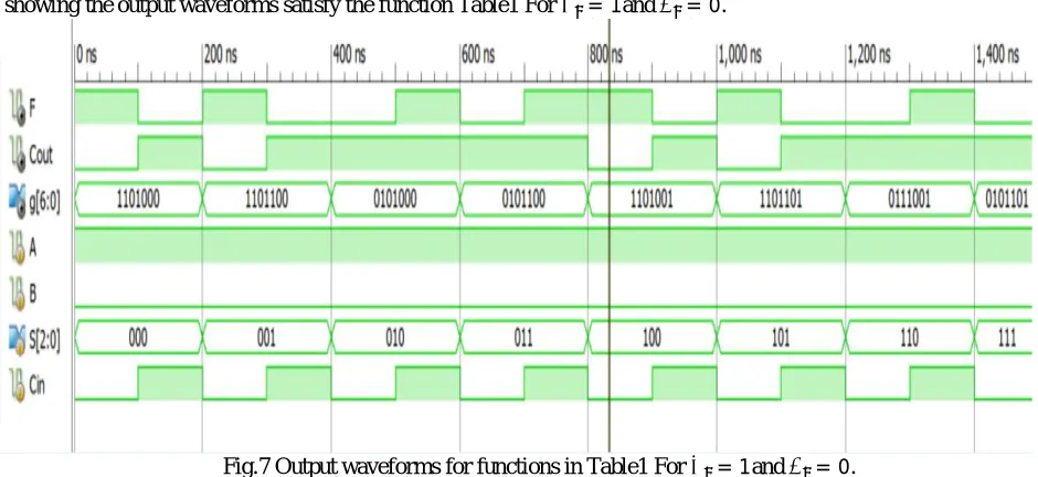
[image:5.612.80.550.310.526.2]The Fig.7 showing the output waveforms satisfy the function Table1 For = 1and = 0.
Fig.7 Output waveforms for functions in Table1 For = 1and = 0.
There are basically two input operands and , depending on the values of , , and we can get different Arithmetic and
[image:5.612.51.509.582.740.2]logic operations on and as per the above Table 1.
Table 2Performance Parameters
Performance parameters Proposed
1-bit ALU
Existed 1-bit ALU
Constant inputs
3 5
Garbage outputs
6 11
Gate count
6 9
Quantum cost
The Verilog code is synthesized using Xilinx RTL compiler for the delay analysis of proposed reversible ALU.Table 3 shows the propagation delay analysis of proposed 1-bit ALU and existed 1-bit ALU[5] and Conventional 1-bit ALU. It can be concluded that proposed reversibleALU design shows higher reduction in delay in compared with existed design and conventional design
Table 3Comparison of Dealy
ALU Designs Propagation delay
Proposed 1-bit reversible ALU 6.92 ns
Existed 1-bit reversible ALU 7.17 ns
Coventional 1-bit ALU 8.133 ns
IV. CONCLUSION
In this paper, 1-bit reversible ALU i.e. reversible control unit and reversible full adder unit, using reversible HNG logic gates has been implemented on Xilinx ISE design suite 14.7 tool. We have compared this proposed design with the existing designs in terms of reversible gates used, Garbage outputs, Quantum Cost, constant inputs and number of logical & arithmetic functions. Arithmetic & logical unit using reversible control unit has also great improvement over existing designs.It has 6 gate count, 6 garbage output, 22 Quantum cost, 3 constant input which are less in compare to existing design. Reversible computing has its great significance in reducing the complexity of the digital circuits. Reversible logic has different areas for its application, those are low power CMOS, quantum computing, nanotechnology, cryptography, optical computing, DNA computing, digital signal processing, quantum dot cellular automata, communication and computer graphics.In future we candesign complete reversible computer architecture with the help of proposed designs.
0 5 10 15 20 25 30
Gate count Garbage
outputs
Constant inputs
Quantum cost
Comparison of Performane Parameters
Proposed 1-bit ALU Existed 1-bit ALU[5]
6 6.5 7 7.5 8 8.5 Proposed 1-bit reversible ALU Existed 1-bit reversible ALU
Coventional 1-bit ALU
Comparison of Propagation delay
REFERENCES
[1]. R. Landauer, “Irreversibility and Heat Generation in the Computational Process”, IBM Journal of Research and Development, vol. 5, pp. 183-191, 1961. [2]. C.H. Bennett, “Logical Reversibility of Computation”, IBM Journal of Research and Development, pp. 525-532, 1973.
[3]. Y. Jiang, A. AlSheraidah, Y. Wang, E.Sha, and J. Chung, “A Novel MultiplexerBased LowPower Full Adder”, IEEE Transactions on circuits and systems -II: express briefs, vol. 51, No. 7, 2004.
[4]. A. P. Chandrakasan, S. Sheng, and R. W.Brodersen, “Low-Power CMOS Digital Design”, IEEE journal of Solid –State circuits.Vol.27,No. 4, April 1992. [5]. D. Maslov and G. W. Dueck,“Reversible Cascades With Minimal Garbage” , IEEE Transaction on computer-aided design of integrated circuits and systems,
vol. 23, No. 11, November 2004.
[6]. V. V. Shende, A. K. Prasad, I. L. Markov, and J. P. Hayes,” Synthesis of Reversible Logic Circuits”, IEEE Transaction on computer-aided design of integrated circuits and systems, vol. 22, No. 6, June 2003.
[7]. Y. V Rentergem and A. De Vos, “Optimal Design of a Reversible Full Adder”, International Journal of Unconventional Computing, vol. 1, pp. 339 – 355. 2005.
[8]. H. Thapliyal, M. B.Srinivas, “Novel Design and Reversible Logic Synthesis of Multiplexer Based Full Adder and Multipliers”, Forty Eight Midwest Symposium on Circuits andSystems, vol. 2, pp. 1593 –1596 2006.
[9]. R. K. James, S. T. K, K Poulose Jacob, and S.Sasi, “A New Look at Reversible Logic Implementation of Decimal Adder”, The International Symposium on System-On-Chip, 2007.
[10].L. Ni, Z. Guan, and W. Zhu, “A General Method of Constructing the Reversible Full-Adder”, Third International Symposium on Intelligent Information Technology and Security Informatics, pp.109-113, 2010.
[11].R. H G al, “Low Power Reversible Parallel Binary Adder/Subtractor”, International journal of VLSI design & Communication Systems (VLSICS) Vol.1, No.3, September 2010.
[12].Md. Saiful Islam, M. M. Rahman, Z. begum, and M.Zulfiquar Hafiz, “ Efficient Approaches for Designing Fault Tolerant Reversible Carry Look-Ahead and CarrySkip Adders”, MASAUM Journal of Basic and Applied Sciences, Vol. 1, No. 3, October 2009.
[13].L. Gopal, N. M. Mahayadin, A. K. Chowdhury, A. A. Golalai, A. K. Singh,“Design and synthesis of Reversible Arithmetic and logic unit”, IEEE 2014 International Conference on Computer, Communication, and Control Technology (I4CT 2014), pp. 289-293, September 2014.
[14].A. Dixit, V. kapse, “Arithmetic & Logic unit (ALU) design using Reversible control unit”, International Journal of Engineering and Innovative Technology (IJEIT), Vol. 1, pp. 55-60, June 2012.
[15].M. S. Sankhwar, R. khatri, “Design of High Speed Low power Reversible Logic Adder Using HNG gate”, International Journal of Engineering Research and Applications, vol. 4, pp. 152-159, January 2014.