SLAVE EMULATOR HARDWARE
REFERENCE MANUAL
SLAVE EMULATOR HARDWARE
REFERENCE MANUAL
2302-5003-01
October 1982
Kontron Electronics, Inc. 5730 Buckingham parkway
UVISION BIS1'ORY
Title
Slave Emulator Hardware Reference Manual
ULA'I'BD PUBLICATIONS
ADS Installation And Maintenance Floppy Disk Drives
EPROM Programmer
Slave Logie Analyzer
Slave Emulator Reference Manual
Copyright 1982 by Kontron
Number
2302-5003
2300-5003 2300-5007 2300-5035 2302-5012
2302-5000
Date Notes
CORRECTION
In our current system
conf~gurationtthe Kontron Logic Analyzer (KLA) unit or
the
Kontl:'on
DevelopmentSystem
(KDS)unit
rerlaces the ADS console as the host unit.The Kontron Slave Emulator (KSE) replaces the
Slave!mulator.
Figures 1-1 and 1-3 of this document
stillshow the
older ~t>S console,and the
Slave
F..mulo.tor
chassis. Theseillustrations
wUl be upd.ated in the next~ev19ion
of
thismanual.
Untilthen, please substitute
thenew
equ1~entdes1.gna tions
fof'
the
old
names.The
1nforma tional
contentof
thePREFACE
The scope of this manual is limited to the basic Slave Emulator. Microprocessor specific systems are defined in the Supplements to this manual.
Chapter 1, Introduction, describes the Emulator Control Unit hardware and specifications.
Chapter 2, ·Emulator Setup And Checkout, describes preliminary checks, system interconnections, and limited Emulator Control Unit system test.
Chapter 3, Maintenance, characterizes preventive maintenance, troubleshooting information t and
disassembly instructions. Diagrams and supporting data are included.
Chapter 4, Theory Of Operation, narrates the function of Emulator boards such as the interface processor, breakpoint, and memory boards.
Please note that a Documentation Reply Card is inserted at the back of this manual. When you complete and return it, you help us produce better documentation for you.
WAlUIING
CONTENTS
CllAPTD. 1 - INTRODUCTION 1.1
1.2
1.4
PURPOSE AND SCOPE OVERVIEW
1.2.1 Slave Vs Traditional In-Circuit Emulation 1.2.2 Emulation Objectives
1.2.3 Target System Substitution 1.2.4 The Emulation System
HARDWARE DESCRIPTION 1.3.1 Emulator Cabinet 1.3.2 Emulator Probe 1.3.3 Emulator Boards 1.3.4 External Probe
1.3.5 Internal Emulator Cabling SPECIFICAnONS
1.4.1 Emulator Cabinet 1.4.2 External Probe
1.4.3 Performance prologue CllAPTER 2 - INSTALLATION AND CHECKOUT
2.4 2.5
INSTALLATION DOCUMENTS
INSPECTING AND SETTING UP THE SYSTEM CONFIGURATION REQUIREMENTS
2.3.1 ADS Configuration
2.3.2 Emulator Configuration Requirements SYSTEM INTERcoNNECTIONS
GETTING STARTED 2.5.1 Conventions
2.5.2 Powering Up The System 2.5.3 Initializing The Emulator 2.5.4 Switch Emulator
2.5.5 Debugger Commands
EXTERNAL PROBE FUNCTIONAL DESCRIPTION
CBAPTD. 3 - MAIftERAHCE
SYSTEM MAINTENANCE AND TROUBLESHOOTING 3.1.1 Emulator Malfunctions
3.1.2 Floppy Disk Unit Malfunctions 3.1.3 ADS Malfunctions
EMULATOR TROUBLESHOOTING CHARTS DISASSEMBLY INSTRUCTIONS
3.3.1 Rear Panel Removal 3.3.2 Board Removal
3.3.3 Enclosure Cover Removal
3.3.4 Front Panel/Power Supply Removal
CHAPTER 4 - THEORY OF OPDAnON
4.4
4.5
4.7 4.8
SCOPE
GENERAL DESCRIPTION
SUBSTITUTING THE EMULATION PROCESSOR FOR THE TARGET SYSTEM'S PROCESSOR
MONITORING THE EMULATION PROCESSOR 4.4.1 Logic Analyzer Board
4.4.2 Breakpoint Board
4.4.3 Emulator Personality Board 4.4.4 Simulation Memory
CONTROLLING THE EMULATION PROCESSOR 4.5.1 Emulator Personality Board 4.5.2 Interface processor Board EMULATION TECHNIQUES
4.6.1 Initialization 4.6.2 The Execute Command 4.6.3 The Halt Command
4.6.4 Storing Data and Screen Updating 4.6.5 Single Step
4.6.6 Memory Mapping
4.6.7 External Control Lines 4.6.8 Breakpoints
BACKPLANE CONNECTIONS TO THE EMULATOR BUS INTERFACE PROCESSOR BOARD
4.8.1 ZSO Processor 4.8.2 Bus Interface Unit
4.8.3 Emulator Bus Addressing for IP Accesses 4.8.4 Emulator Bus Arbitration
4.8.5 Bus Fault Timer
4.8.6 Direct IP Access To Simulation Memory 4.8.7 Memory Mappers
4.9 4.10 4.11 4.12 4.13 4.14 4.15
4.8.8 Dynamic RAM Refresh 4.8.9 PROMS
4.8.10 I/O Lines 4.8.11 Serial Ports 4.8.12 System Interrupts 4.8.13 Syst.em Adqress Latches 4.8.14 PIO Latches
4.8.15 Backplane Address Bits EXTERNAL PROBE
BREAKPO INT BOARD
4.10.1 General Description 4.10.2 Registers And Ports 4.10.3 System Addresses
4.10.4 Operation of Breakpoint RAMs 4.10.5 Breakpoint Counters
4.10.6 Breakpoint Mode Register
4.10.7 Interface Processor Breakpoint Interrupt LOGIC ANALYZER
4.11.1 Logic Analyzer Operation 4.11.2 External Controls
4.11.3 Logic Analyzer Initialization 4.11.4 Time/Cycle Counter Operation SIMULATION MEMORY
4.12.1 Block Mappers
4.12.2 Word/Byte Memory Configuration DYNAMIC MEMORY
4.13.1 Block Mappers 4.13.2 Memory Array 4.13.3 Control Logic
4.13.4 Parity Generation and Checking 4.13.5 Refreshing
4.13.6 Write Protect and Internal/External Memory Mappers
DYNAMIC MEMORY INTERFACE WITH IP BOARD 4.14.1 Programming The Block Mappers
4.14.2 Write Protect and Internal/External Memory Mapper EMULATOR PERSONALITY
4.15.1 Test Memory
4.15.2 Emulator Bus Arbitration 4.15.3 Pre-Fetch Tracking
4.15.4 Timing Signals 4-15.5 Mapping
APPENDIX INDEX
KORD.ON SERVICE NUMBERS
ILLUSTRATIONS
FIGURE PAGE
1-1 Multi-Emulation Station 1-3
1-2 External Probe 1-5
1-3 Internal Cabling 1-7
1-4 Buffer Circuit 1-11
2-1 System Interconnections 2-3
2-2 Emulator Executive Display 2-6
2-3 Enter SW1 2-7
2-4 Switch Command Display 2-8
3-1 Executive Test Symptoms 3-3
3-2 Switch Display Symptoms 3-4'
3-3 Exploded View 3-5
3-4 Rear Panel Removal 3-6
3-5 Board Removal 3-7
3-6 Enclosure Cover Removal 3-8
3-7 Front Panel Details 3-9
4-0 Slave Emulator Block Diagram 4-0
4-1 Memory Mapping 4-8
4-2 Buffer Control 4-9
4-3 Emulator Bus 4-11
4-4 Interface Processor - BIU Timing 4-18
4-5 SYNC*/Breakpoint 1 4-23
4-6 System Address Register 4-25
4-7 Breakpoint Status Register 4-27
FIGURE
4-9 4-10 4-11 4-12 4-13
TABLE 1-1 4-1
Breakpoint Mode Register
Breakpoint Address RAMs (Greater Than) Breakpoint Address RAMs (Less Than) Breakpoint Control Logic
Buffers/Transceivers
TABLES
Internal Cables Buffer Control
PAGE 4-29 4-31 4-32
4-34
4-48
PAGE
CHAPTER 1
INTRODUCTION
1. 1 PtmPOSB AND SCOPE
The purpose of this manual is to acquaint the user with Kontron's Slave Emulator. Information is given on installation, checkout, maintenance and theory of operation.
1.2 OVERVIEW
1.2.1 SLAVE VDSUS TRADITIONAL IN-CIRCUIT EMULATION
Traditional in-circuit emulation is less than ideal. Often, the processor under test is restrained from running at full speed, or some of its memory is tied up by the emulation hardware, or the system under test must be halted to conduct debugging. operations. These limitations are removed when using slave in-circuit emulation, because the multiprocessor, and the multiple bus organization of the Kontron Slave Emulator allows full-speed emulation of 8-bit, or 16-bit microprocessors.
Note that from this point on, throughout this manual, the Kontron Slave Emulator is referred to as the Emulator.
1.2.2 EHULATIOR OBJECTIVES
The two main objectives of the emulation process are:
a. Substitution of an Emulation processor for the target system's processor.
1.2.3 TARGET SYSTEM SUBSTITUTION
The Emulator substitutes an identical processor for the target system's processor. To eliminate critical physical distances, this Emulation Processor is housed in a sm~ll portable chassis called a Probe, which is connected by a short cable to the target system's vacant microprocessor socket. The signals into and out of the Emulation Processor can be easily relayed from the Probe to the target system's socket.
1.2.4 THE EMULATION SYSTEM
The Development System consists of a 2300 Console with keyboard and CRT display, a dual floppy disk system, supporting software/firmware, and other
parts.
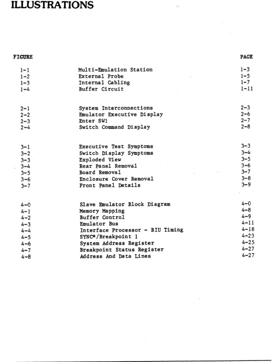
One of the advantages of Slave Emulation is the ability to emulate up to four microprocessors si..:1ultaneously through one Development System. This provides a low-cost and efficient means to emulate a multiprocessor environment. Up to four processors can be monitored, and controlled from one station. All Emula tors can be synchronously hal ted . from a single event in any of the Emulators or a combination of several events in one or more of the Emulators. This is a powerful debugging tool in a multiprocessor environment. See Figure 1-1, Multi-Emulation Station.
1.3 HARDWARE DESCRIPTION
1 .3. 1 EMULATOR CABINET
Wi thin the Emulator cabinet is an eight slot card cage which must have a minimum of three boards installed: an Interface Processor Board, a Breakpoint Board, and a Personality Board. The maximum number of boards is eight, adding an optional Logic Analyzer, and up to four Simulation Memory boards. When changing to a different Emulator configuration, access to the boards is through the rear panel.
1.3.2 EMULATOR PROBE
The probe is a buffer device which brings the Emulation Processor as close as possible to the target system to prevent loss of signal integrity. It is microprocessor dependent, and serves as the interface between the microprocessor being emulated, and the Emulator Personal:' L - Board. A more
EMULATOR
~
-
-PORT A
~
...-.. IN
SLAVE
-DISK u N EMULATOR MICROPROCESSOR
PORT B ~ SOCKET
CO)
OUT ..
,
N ,
-en
-
-.a:
--
r - ' --
-,PORT A
-
IN ~-I- SLAVE
PRINTER
-
a:0 EMULATOR
a.. .. 2 ~
-..J
""'""!-
-
-!f a:
u.J
-
-en
/
/
SLAVE ~-EMULATOR
USER
.. 3 ~
-
SYSTEM-2300
-
-ADS ~
-SLAVE
/
EMULATOR .. 4 ~-' " - -
-
[image:16.612.49.559.30.762.2]1.3.3 EMULATOR BOARDS
The Emulator holds a maximum of eight boards. Each board, with its component side up, can be inserted into anyone o·f the eight interchangeable slots in the card cage. The backplane of the card cage is a parallel bus system, designed to bring information from the microprocessor and the target system to
the Emulator.
The basic boards and minimum configuration shipped with the Emulator include: 1. Interface Processor Board The IP responds to commands from the
console, controls the Emuiation processor and returns data to the user.
2.
3.
Breakpoint Board The Breakpoint board has breakpoints that can break on parameters such as memory, I/O, execution/fetch, and a pass counter.
four hardware address, data,
Personality Board (Microprocessor specific) This board is the interface between the emulated processor's bus and the Slave Emulator. In addition, it dire~tly controls all emulation processes. Optional boards are Simulation Memory, Dynamic Memory when supported, and a Logic Analyzer. Simulation Hemory is available from 16K to 512K bytes of memory. The functions of these boards, and the entire system are described in Chapter 4.
The addi tion of the Simulation Memory Board and the Logic Analyzer board to the Slave Emulator configuration allows debugging without involving the target system memory. Simulation Memory board can simulate ROM, without having to program ROMs.
Logic Analyzer simplifies troubleshooting by providing detailed waveform display and cycle data display_ This allows the user to view bus data during program execution.
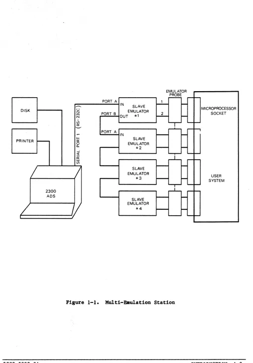
1.3.4 EXTERNAL PROBE
The External Probe, see Fiaure 1-2, External probe, is a multifunction device that works together with the Breakpoint, and optionally with the Logic Analyzer. It brings in four external signals, called external lines in the breakpoint parameters, from any TTL compatible source. These external lines can be used as breakpoint qualifiers or they can be traced by the Logic Analyzer.
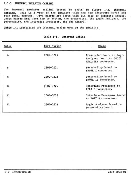
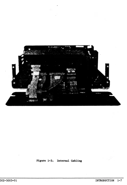
1.3.5 INTERNAL EMULATOR CABLING
The internal Emulator cabling system is shown in Figure 1-3, Internal Cabling. This is a view of the Emulator with the top enclosure cover and rear panel removed. Five boards are shown with six sets of separate cables. These boards are, from top to bottom, the Breakpoint, the Logic Analyzer, the Personality, the Interface Processor, and the Memory.
Table 1-1 identifies the internal cables used in the Emulator. Table 1-1. Internal Cables
cable Part Nunber Usage
A 2302-0225 Brea.~point board to Logic
Analyzer board to LOGIC ANALYZER connector.
B 2302-0221 Personality board to
PROBE I connector.
C 2302-0222 Personality board to
PROBE II connector.
D 2302-0226 Interface Processor to
PORT B connector.
E 2302-0026 Interface Processor board
t.o PORT A connector.
F 2302-0234 Logic Analyzer board to
[image:19.617.38.564.75.778.2]1.4 SPECIFICATIONS 1.4.1 EMULATOR CABINET Outline Dimensions:
Width: Height: Length:
16.1" (40.64cm) 7.6" (19.3cm) 18.2" (46.23cm) Weight: 40 lbs (18kg)
Cooling: Forced air
Operating Ambient Temperature: 0 to 40 C (32 to 104 F) Storage Ambient Temp~rature: -50 to 125 C (-58 to 257 F) Power system:
In put AC line vol tage,: a. 90-130 VAC b. 200-260 VAC
Input line voltages are a factory option. Input current:
Less than 5 amps @ 115vac Less than 2.5 amps @ 2.30vac Single phase 3-wire system
47 - 440 Hz
Note that the Emulator's power system is preset, at the factory, to your specifications.
Power Dissipation: 350 watts maximum Circuit Protection:
1.4.2 EXTERNAL PROBE
Outline Dimensions: Width:
Height: Length:
2 .7 5" (6.98 5c m) .625" (1.587 Scm) 2.75" (6.985cm) Weight: 7 ounces (198gm) Cooling: Convection air
1 .4.3 PERFOBMANCE PROLOGOE
The most important link in any Emulator is the interface· between the user's target system and the Emulator. Systems are designed with the assumption that a microprocessor will reside on board. The introduction of a length of cable and buffer circuitry (the Emulator) between the 1I1i.croprocessor and its socket may create problems. Wirewrapped prototypes, if not carefully laid out, can be very noisy. The introduction of a length of cable may make the system inoperable. It is important therefore that prototypes have a good power and ground grid. Wirewrapped boards should have the power and ground system soldered down. Systems operating within the guidelines of standard TTL logic will not encounter problems with an Emulator. problems may be encountered with noisy systems.
CAUTION:
Signal Pulse Delays
The Emulator may not be used with a target which is floating with respect to ground. _ This float is measured as the Voltage between target ground and chassis ground. The Emulator is referenced to standard earth ground. The Emulator power supply returns are attached to the chassis ground. Thus the microprocessor plug ground pins are referenced to chassis ground.
IF THE TARGET IS FLOATING WITH RESPECT TO EARTH GROUND, SEVERE DAMAGE TO THE EMULATOR PROBE AND TARGET MAY OCCUR.
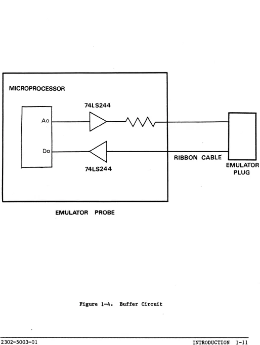
Each signal at the Emulator Plug is buffered in both directions in the Emulator Probe. A signal such as AO in Figure 1-4, Buffer Circuit, delivered to the Emulator Plug through the buffer tends to arrive typically 9 to 10 nanoseconds later. There is a similar delay in the signal shown as DO in Figure 1-4" going to the microprocessor from the target system. For request/response operations such· as memory reads, these delays are additive,and can result in a total delay of 9 to 18 nanoseconds. Detailed timing specifications are given in the supplement for each subsystem.
MICROPROCESSOR
74l.S244
Ao
~
V
Do
/
'"
RIBBON CABLEEMULATO 74LS244
PLUG R
EMULATOR PROBE
[image:24.612.57.571.89.769.2]CHAPTER 2
INSTALLATION AND CHECKOUT
2.1 INSTALLATION DOCUMENTS
Included in the shipment are four important installation documents: Cover Letter
Installation/Quality Report Configuration Checklist User Registration Card
The top half of the Installation/Quality Report is filled in by Kontron before the equi tment leaves the factory. The bottom half of this form is filled in by Kontron installation personnel at the customer site. Additional comments can be made by the customer in the spaces provided at the bottom of the form, and then signed off.
The configuration checklist describes all the equipnent included with each shipment from Kontron. This form is signed and dated by factory representatives. A complete list of the items sent in the shipment is provided for the customer to check off when the system is received. In case of any discrepancy, contact your Kontron representative.
2.2 INSPECTING AND SETTING UP THE SYSTEM
After removing the Emulator from the carton, save all packaging materials in case the system requires shipping at a later date. An inventory of the. shipment received should be taken immediately after all parts are removed from their shipping containers. Inspect the equipment for evidence of shipping damage to housing, panel controls, or cables.
2.3 CONFIGURATION REQUIREMENTS
If the Emulator being installed will be used in an already operational Development System that was previously set up for the Emulator, or has been just received from the factory, the configuration of the boards need not checked. If the Development System has not been used for emulation previously, it should be setup according to the following requirements.
2.3.1 ADVANCED DEVELOPMENT SYSTEM CONFIGURATION
For Emulator operation, the system configuration must include, as a minimum, 64K bytes of memory, a Z80 board, and an MPIO board.
2.3.2 EMULATOR CONFIGURA'i'ION REQUIREMElfIS
The Emulator boards mutt be configured for the microprocessor being emulated. These are set correctly at the factory for the Emulator Subsystem. However, they will require reconfiguration if the the Personality board in the Emulator, is changed. Correct configuration for each microprocessor is given in the specific Hardware Supplement for that processor.
2.4 SYSTEM INTERCONNECTIONS
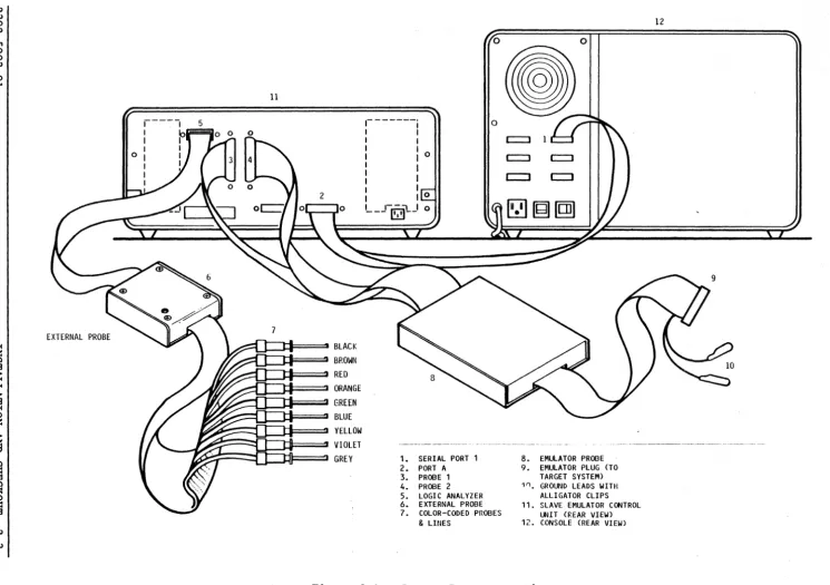
To install a single Emulator refer to Figure 2-1, System Interconnections, and connect the subsystems together as follows:
a. RS-232 Cable. Connect one end to Port A (input) on the Emulator; the other to Serial 1 on the Developement System. Screw the connectors in place.
b. Probe. Connect the two 50-pin connectors (the 72-inch cables) from the Emulator Probe box to Probe 1 and Probe 2 keyed connectors, on the Emulator.
Note that if more than one Emulator is being installed on the same console, the Emulators must be daisy chained as follows:
N W o N I \J1 o o w I o ... N I w
EXTERNAL PROBE
11
U=J:I===:I BLACK
BROWN RED ORANGE GREEN BLUE YELLOW
~~=:(]=l:i==:=:J VIOLET
GREY
o
,---j
I I
I I
I I
I I 0
I I
l
II I
I 10
L_T~!...J 0
1. SERIAL PORT 1 2. PORT A 3. PROBE 1 4. PROBE 2 5. LOGIC ANALYZER 6. EXTERNAL PROBE 7. COLOR-CODED PROBES
& LINES
o
8. EMULATOR PROBE 9. EMULATOR PLUG (TO
TARGET SYSTEM)
11) GROUND LEADS WITH
ALLlGATOR CLIPS 11. SLAVE EMULATOR CONTROL
UNIT (REAR VIEW) 12. CONSOLE (REAR VIEW)
[image:27.796.24.769.50.575.2]2.5 GETTING STARTED
The following checkout procedures wnich are performed without a target system, will acquaint you with some of the most commonly used Emulator commands. If any problems are found while executing this procedure, contact your local representative for further assistance.
2.5.1 CONVENTIONS
The following conventions are used to key-in characters, statements, and commands.
LETTERS
SPECIAL KEYS
Commands and statements are composed of letters and special characters. They are typed in uppercase and must be exactly as shown.
If a special character key is required, it will be enclosed in angle brackets.
Example 1: <RETURN) means press the RETURN key on the keyboard.
Example 2: JM<RETURN) means key-in the letters JM,
then press the RETURN key.
Note that the angle brackets should not be typed. They only show syntax and are not part of any command or required input.
BLANKS No BLANKS are allowed within system commands.
2.5.2 POWERING UP THE SYSTEM
a. Set the ON/OFF power switch at the rear of the system to ON.
If the following procedure, or any portion of i t fails, refer to Chapter 3,
MAINTENANCE •
2.5.3 INITIALIZING THE EMULATOR
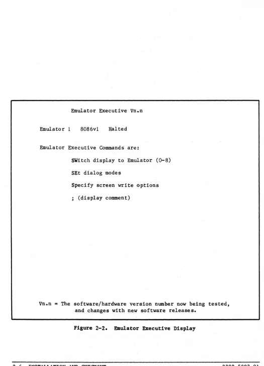
The Emulator must be set to a starting position in every case, regardless of processor type. The response to the initializing procedure is the same, except the type of microprocessor displayed changes according to the Emulator personality used. An example of the procedure, using the 8086, follows:
a. Press the <RESET) button on the Emulator.
b. Insert the 8086 Emulator System File diskette (Part No. 2300-6081-02) into Drive O.
c. Enter JS<RETURN>.
Emulator Executive Vn.n Emulator 1 8086v1 Halted Emulator Executive Commands are:
SWitch display to Emulator (0-8) SEt dialog modes
Specify screen write options ; (display comment)
Vn.n
=
The software/hardware version number now being tested, and changes with new software releases. [image:30.621.32.558.41.768.2]2.5.4 SWITCH EMULATOR
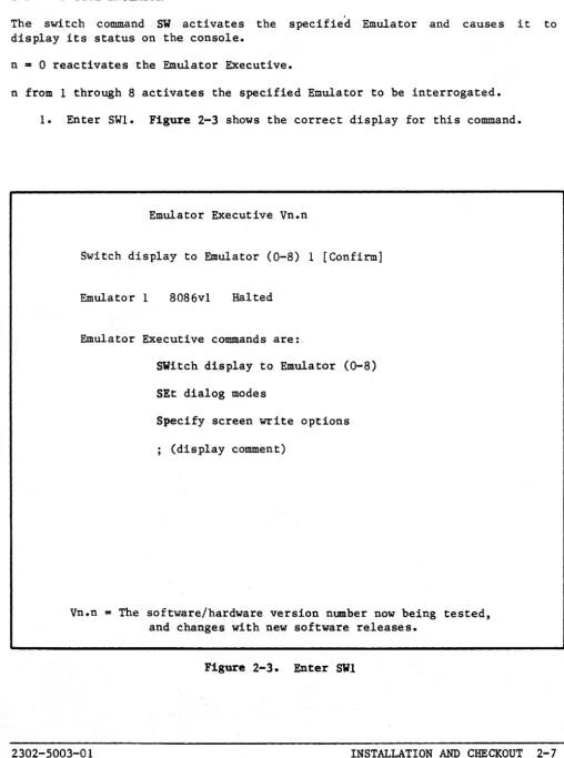
The switch command SW activates the specified Emulator and causes it to display its status on the console.
n
=
0 reactivates the Emulator Executive.n from 1 through 8 activates the specified Emulator to be interrogated. 1. Enter SWI. Figure 2-3 shows the correct display for this command.
Emulator Executive Vn.n
Switch display to Emulator (0-8) 1 [Confirm] Emulator 1 80B6vl Halted
Emulator Executive commands are:
SWitch display to Emulator (O-B)
SEt dialog modes
Specify screen write options ; (display comment)
Vn.n
=
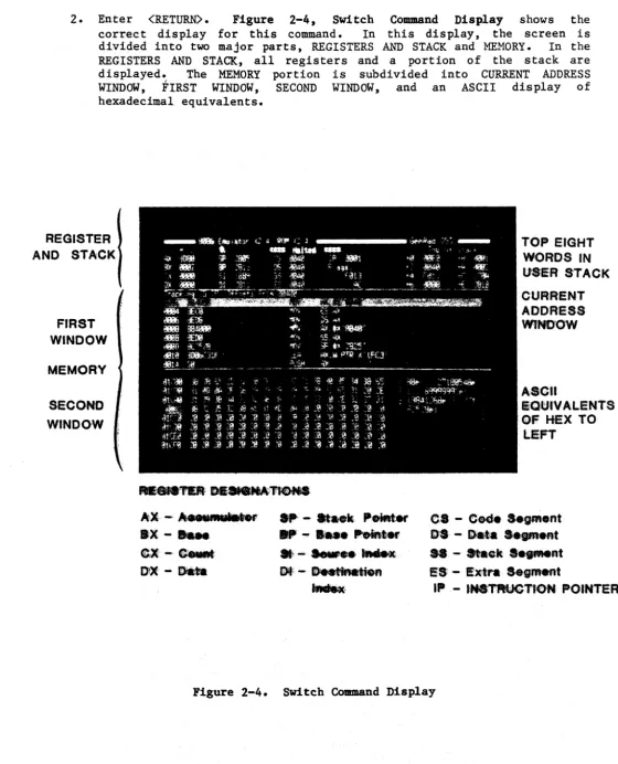
The software/hardware version number now being tested, and changes with new software releases. [image:31.624.47.556.97.780.2]2. Enter <RETURN>. Figure 2-4, Switch Command Display shows the correct display for this command. In this display t the screen is
divided into two major parts, REGISTERS AND STACK and MEMORY. In the REGISTERS AND STACK, all registers and a portion of the stack are displayed. The MEMORY portion is subdivided into CURRENT ADDRESS WINDOW, FIRST WINDOW, SECOND WINDOW, and an ASCII display of hexadecimal equivalents.
REGISTER AND STACK
FIRST WINDOW
MEMORY
SECOND
WINDOW
AX- . . .
w
ax- ....
e;.'f-
C ....[)J)IE - ~
p - _ ••
k Peiat_.. - _. Po.!'_
.~-"'e.~ Ii)lf< - f)eet!inatioA~
TOP EIGHT WORDS IN URR STACK
CURRENT ADDR,ES$
WINDOW
A,scn
eOt.nVALENTS
.OF HEX TO LEFT
ea -
Cede h ... e,ntil»)8 - Deta $8fIjfft.nt
H - .taek . . .
f.lt I!S: - !Ext'"a Segf!1!teAtlID . - IlNe'TPtlUGTrON POINTER
[image:32.626.16.576.74.766.2]2.5.5 DEBUGGER COMMANDS
When in the debugger mode, commands can be entered in any order. The commands available can be referenced at any time by entering a <?) or <HELP). Either command will display the help file, which lists all commands. In addition, once a command has been entered, a <1) can be entered again for additional information on the current command.
I. To begin, enter the Edit Simulation Memory Command EDS<RETURN>. The display will switch to the Simulation Memory configuration map. If
Simulation Memory was not ordered or included in your unit, this procedure cannot be executed. The Simulation Memory Map indicates the number of blocks available, the size of the blocks (8K, 32K or 64K) , and where they are presently mapped. When the system is initialized, all blocks are mapped contiguously from O. Make sure that there is at least 16K bytes of Simulation Memory available. The Debugger prompts the block which you choose to relocate. The next prompt would be what starting address you want to relocate it to. In this manner, Simulation Memory blocks can be relocated to any 8K or 32K byte block boundary within the microprocessor's address space. In this checkout procedure the aim is to check on the current status of Simulation Memory without altering it. Press the <CAN) key to return to the Debugger display.
2. The counterpart to Edit Simulation Memory command is Edit Target Memory. Enter EDT<RETURN). The display will switch to the Target Memory map. This map indicates which memory spaces are internal and which are external. Blocks of memory as small as 256 bytes can be mapped internally or externally by answering the series of prompts. When the system is initialized, it maps all of the memory spaces internally. If there is no target system connected, all of the memory space would be mapped internally. Press the <CAN> key to return to the Debugger.
4. One of the memory window options is to display from an offset or absolute address. The Emulator, when emulating segmented microprocessors such as the 8086, will initialize with the offset mode enabled in the upper window. To enable the offset mode the command WIndow is used and the option OFfset is selected. The offset value for the memory window is set using the OFfset command.
5. Programs can be stored into memory in two ways. They can be loaded down from disk or they can be entered via the keyboard. In this example we will store a short loop by using the STore command. The STore command will store data in bytes starting at the current memory location. The current memory location is indicated in one of the memory windows by the reverse video display across the entire memory window. In this case data will be stored at 500. In the next step, proceed to the section for the microprocessor you are emulating. 6. A. 8086
The 8086 has a code segment register. The upper memory window will track the instruction pointer and code segment registers. Set the code segment register CS to 0000. To do this use the SEt register command. Enter SEt register CS=OOOO.
Store the following bytes.
Enter SToreFF CO A3 50 05 EB F9 (RETURN>(RETURN)
Notice that the upper memory window now has the above opcode displayed in both machine code and disassembled shown below.
500 502 505
FFCO A35005 EBF9
Proceed to step 7. B. 68000
INC
MOV JMP
AX
W PTR X'OSSO' ,AX
SHORT X'OSOO'
The 68000 has a Trace bit that will generate an interrupt after every instruction if it is set in the Status Register SR. Set the Status Register to 2700 by entering SEt register 2700 (RETURN> to disable the Trace bit.
C.
Enter STore52 80 31 CO 05 50 60 F8 (RETURN> (RETURN>
Notice that the upper memory window now has the above opcode displayed in both machine code and disassembled as shown below. 500 5280 ADDQ.L 111 ,DO
502 31C00550 MOVE.W DO,000500 506 60F8 BRA 000500
Proceed to step 7. Z8000
Set the Fcw by entering SEt register Fcw 4000. Store the following bytes.
Enter SToreA9 10 6F 01 ~5 50 5E 08 05 00 (RETURN> (RETURN>
Notice that the upper memory window now displays the machine code and its disassembly as shown below.
500 502 506
A9IO INC R1,#I 6FOI0550 LD 5E080500 JP Proceed to step
7.
0550,RI UN,0500
D. 6502
Store the following bytes.
Enter SToreEE 05 50 AD 05 50 4C 00 05 (RETURN>
<RETURN>
Notice that the upper memory window displays the machine code and its disassembly as shown below.
500 503 506
EE0550 AD0550 4C0005 Proceed to step 7.
INC LDA
JMP
E. 6809
Store the following bytes.
Enter STore4C
B7
05 50 20 FA<RETURN> <RETURN)
Notice that the upper memory window now displays the machine code and its disassembly as shown below.
500 4C
501 B70550 504 20FA
INC A
STA 0550 BRA 0500 Proceed to step 7.
F. 280
Store the following bytes.
Enter STore3C 3A 50 05 C3 00 05
<RETURN> <RETURN)
Notice that the upper memory window displays the machine code and its disassembly as shown below.
7. When executing a program, several memory windows can be tracked. The mnnber of memory windows (1 to 4), and their orientation is selected by the SCreen command. This command selects 8 memory window display formats. To find ·out what the optional formats are tenter SCT. The display will switch to the screen format help display. Press the <CAN> key to return to the Debugger display. When initialized the Emulator selects format 2.
8. While the Emulator is executing, the memory windows are updated every time a command string is completed or a breakpoint is reached. To update the screen periodically a <RETURN> can be entered to force updating. Memory windows can track a specific location or track at a register. By entering Display expression, the memory window will track a specific memory space. Display @ expression is used to track a register. These commands are implemented on the current memory window. The current memory window is selected by pressing the <TAB) key. In this example the top memory window is tracking the program counter and the bottom window is displaying above and below
0000.
9. Each memory window can display memory data in two formats: hexadecimal or symbolic. This is selected by the WIndow command. In this example the upper window is displaying in the symbolic format and the lower window is in the hexadecimal format.
10. The program counter is now at .500 and the upper memory window is tracking the program counter at 500. The EXecute command can now be invoked and the Emulator will begin execution at the program counter. Enter EXecute <RETURN). The message RUIllling will appear at the message line on the display. Press the <RETURN> key several times and notice that the program counter t the incremented register, and the upper memory window are updated with each stroke of the return key.
11. The Halt command forces the Emulator to cease execution of user's code and updates the Debugger display to the point where the processor is halted. Enter Halt<RETURN> Notice that the message line now reads Halted and that the program counter and upper window display are now updated to the next instruction to be executed.
13. The <STEP) key will counter. Press the Single Step appears program counter and instruction.
The four hardware breakpoints give complex breaking options. Enter
(Breakpoint 1,). The screen will switch to the breakpoint 1 status
display. On the left hand side of the screen are the options and on the right hand side of the screen are the current parameter settings for breakpoint 1. Count indicates the number of passes over the breakpoint before a break occurs. Set Count to 32767 by entering (Count 32167).
Address and data can be set to a specific value or X for don't care. Se t addres s to 500 by entering (Address 500) • Da ta should be left at don't care for this example.
External lines are the four external lines from the External Probe. In this example they are set at don't care.
Instruction/Data indicates whether the breakpoint should break on the fetch or the execution of the specified address. For prefetching processors like th~ 8086, this makes a significant difference since the microprocessor can fetch ahead as many as six bytes. When breaking on an instruction, i t should be set to Instruction. When breaking on a data move as in a peripheral access, it should be set to Data. In this example it is set to Instruction.
Read/Write specifies the direction of data flow for the breakpoint. Memory/IO indicates that the break will occur during a memory or
r/o
cycle. For some microprocessors like the 68000, which has nor/o
cycles, this parameter is meaningless, and it is ignored. For this example, it is left at Memory.Halt/Snapshot indicates whether the processor will halt or continue execution after the breakpoint is reached. In this example, it is left at Halt.
Breakpoint 1 should now be set as follows:
Count
=
32767Add
=
00500Data
=
XXXXExt Line
=
XXXX14. Execute the program by entering the EXecute command. Notice the message Stopped at Breakpoint 1 appears on the message line. The program counter and the upper memory window will display the next instruction to be executed by the Emulator. Since prefetch and breakpoint characteristics of different microprocessors are different, each microprocessor will halt at a different point.
15. The .breakpoints can be cleared individually using the BESEt command or all breakpoints can be cleared using the CLear command.
The preceding 15 steps have been an introduction to some of the commands as they might be used without a target system. Three more steps are required to begin emulation with a target system.
1. The Emulator Plug is inserted in place of the microprocessor on the target system. Use caution when plugging the Emulator probe into the target system. Placing the plug in backwards can damage the probe, or cause the target power supply to short to the probe's ground. care should be taken that pins are not bent and that the Plug is inserted in the correct orientation.
2. Some or all of the microprocessor's address space must be mapped externally to gain access to the desired portions of target memory. This is done using the EDit target memory command.
3. Each Emulator Subsystem has target system control lines to the Emulation Processor. These can be enabled, or disabled under the ENable control lines command. It may be necessary to enable some or all of the control lines to the target system depending on the microprocessor and the target system. For example, if the target memory to be accessed is slow J and requires the use of a wait line,
this line should be enabled under the ENable control lines command. When you choose to ignore all interrupts, and DMA processing, leave the ENable control lines disabled.
Additional processor specific information is given in the Supplement for each of the Emulator Subsytems. The Debugger chapter of the Development Manual
2.6 EXTERNAL PROBE FUNCTIONAL DESCRIPTION
The External Probe performs two functions. First function is to provide external breakpoint triggers. These triggers can then be used as a complex trigger for oscilloscopes, or passed on to another Emulator to provide synchronous breakpoints in a multiprocessor emulation environment. The second function of the External Probe is to input four external, TTL compatible conditions to the Breakpoint Board for external break conditioning, and to the Logic Analyzer to be traced with the other Emulation Processor functions.
CHAPTER 3
MAINTENANCE
3.1 SYSTEH MADiTENANCE AND TROUBLESHOOTING
Preventive maintenance is not required on the Emulator as a whole, or on any subsystem unit. When a malfunction does occur, troubleshooting and analysis should first be attempted on a system level. This can best be done by using the system software to examine or interrogate the various units, observing the resulting console displays (and/or ha~d copy if available), then proceeding to correct the operational defect. There are several operational checks to determine if proper procedure has been violated resulting in an error. In addition to the procedures following, please refer to Section 2 in the Supplement for possible errors in configuration or application. Emulator troubleshooting requires the' user to be familiar with total system software and ADS Console programming operations.
3.1.1 EMDLATOR.MALFUNCTIONS
The Emulator unit requires no operational mechanical or electrical preventive maintenance. If trouble develops immediately after any part of the Emulator has been disconnected, or disassembled, recheck the work done.
Error symptoms may have causes outside the Emulator unit. These could be hardware-originated, software-originated, or both. Check to see that the Emulator Probe and Emulator Personality boards are compatible. The software revision number on the Emulator Executive must match the Interface Processor board PROMs. Check the Hardware Supplement Section 2 for correct board configurations.
If any board is suspected as the source of trouble, check first to make sure that all IC's are snug in their sockets.
Check all boards, cables and connectors for a tight fit.
3.1.2 FLOPPY DISK UNIT MALFUNCTIONS
Preventive Maintenance. Procedures for preventive maintenance are detailed in the FutureData INSTALLATION AND MAINTENANCE MANUAL (2300-5003-01).
3.1.3 ADS MALltJRCTIONS
ADS malfunctions, maintenance techniques, and troubleshooting information are found in the FutureData INSTALLATION AND MAINTENANCE MANUAL (2300-5003-01).
3.2 EMULATOR TROUBLESHOOTING ClWlTS
EMULATOR EXECUTIVE TEST ENTER JS(RETURN)
ERROR SYMPTOM
1. No 'Halted' Display X
2. No 'Commands' Display i x
3.· Bl ank Screen I
D E F Gi H
X X
! X
xl
PR()BABLE CAUSE / ; A I/F PROCESSOR PWB
/ B MEMORY PWB
! /
BREAKPOINT PWB~
I
!~I
C,PER~.SONALITY
PWB LOGIC ANALYZER PWBMIN 0 X X X x
I
IX i X i I
:
!i
[image:43.620.54.548.56.744.2]EMULATOR
SWITCH OISPLAY ENTER SW[n]
n=[0-8] !
"
, .' / ! / / / !A, S! C 01
!
i i
! / ,I I ! l / :/ Ei F
I
i
I
!
!
I
! // !
! !
I
! !
I !
i i i i
PROBABLE CAUSE
/ A IIF PROCESSOR PWB
1 _ _ _ _ _ _ _ _ - ;
i B MEMORY PWB
/-C-PERSONAu-r-Y -P-WB---:
o BREAKPOINT PWB
II
E LOGIC ANALYZER PWB~
RS-232 INTERFACE
I
Ii'
F/ I - - - . . . :
/1
/ /
/
-1/
/ G EMULATOR PROBE
/~H-S-Y-S-:::-TE=--M-CA-B-Lc-I N-G---< / ' /'-1 -0
I-S-K-::CET-=T-EJ-O-I-cSK-U--NI~T-:::-I / ! .' I
/1
/ I
i ! !
,I /
!
/
/
L
II •
! ! I
•
! i
J CONSOLE HARDWARE
,/ ,I K CONSOLE CONF 1G.
f /
/ ! ! I i j ! i I
L DOCUMENTATION
M INTERNAL CABLING---:
,-N EMULATOR ,-NOT RESET
---~
o CONSOLE NOT RESET
/ P MPIO STRAPPING
/ Q WRONG S/W VERSION
5i T U
i
I
xl I
i
xl I xl i
1 !
[image:44.623.23.553.16.764.2]3.3 DISASSEMBLY INSTRUCTIONS
Major subassemblies can be readily removed from the main frame. subassemblies are:
a. rear panel b. enclosure cover
c. front panel with power supply
These
The customer should avoid disassembly beyond 'that described in this manual, especially during the warranty period. Only Kontron Service Representatives should attempt further detailed disassembly of this equipment. Figure 3-3, Exploded View, depicts the Emulator subassembly.
BLOWER ASSEMBLY
- , TOP
' ... ~NClOSURE
."~
[image:45.620.58.568.269.736.2]3.3.1 REAR P ANn REMOVAL
To reconfigure the Emulator, it is necessary to remove the rear panel. Refer to Figure 3-4, Rear Panel Removal.
a. Set the ac ON/OFF power switch to OFF and unplug the ac line cord at both ends.
b. Remove all flat cables unscrewing jack-screws, connectors stay parallel.
from their rear alternate between
panel connectors. screws so that
When both c. Remove the four screws shown in the illustration. The rear panel can
now be removed.
-""
BOTTOM ENCLOSURE COVER
'~~l
.
a.o~~AR
PANEL
" -HEX9
NUT ~,
SCREW
[image:46.623.14.560.50.785.2]3.3.2 BOARD REMOVAL
Removing logic boards is a simple operation. Refer to Figure 3-5, Board Removal.
Position thumbs on the board ejectors and pull back, rotating the ejectors outward until the board is pulled away from the Emulator backplane connector. Gently slide the board all the way out.
....
COVER
[image:47.623.48.555.222.773.2]BOARD
3.3.3 ENCLOSURE COVER REMOVAL
Refer to Figure 3-6, Enclosure Cover Removal. It is not usually necessary to open up the interior of the Emulator except to replace the power supply
fuse. '
First, the rear panel must be removed as shown in Section 3.3.1.
the two screws holding the top cover to the corner brackets as illustration, Lift and pull back from the rear as shown. cover-locking guides at the front sides of the chassis.
COVER LOCKING GUIDE
BOTTOM COVER ENCLOSURE
"-'"
COVER LOCKING GUIDE
'-
...
'--SCREW
Figure 3-6. Enclosure Cover Removal
Then, remove shown in the Notice the
TOP COVER ENCLOSURE
[image:48.624.20.555.87.770.2]3.3.4 FlDRT PANEL/POWER SUPPLY iEKoVAL Refer to Figure 3-7, Front Panel Details.
a. Label or mark all wires and wire cables on strip terminals, ON/OFF switch, and RESET switch. Remove the wires and wire cables.
b. Remove the two hexagonal nuts, shown in the illustration, from the front mounting flange on the bottom enclosure. Remove the front panel. c. Remove the four hexagonal nuts holding the power supply mounting flange to the front panel. Remove the power supply assembly from the front panel.
d. Remove the hexagonal nuts holding the power supply to the flange.
FRONT PANEL
POWER SUPPLY
[image:49.617.54.568.272.770.2]RS-232 INTERFACES
_ PORT
r
1PORT 2
I
I
I
I
JI
I
JI
I
I
I
I
I
INTERFACE PROCESSOR EXTERNAL CONDITION PROBE1---BREAKPOINTS ANALYZER LOGIC
BREAKPOINT OUTPUTS
EXTERNAL CONDITIONS
PROCESSOR STATUS
SIMULATION MEMORY
SLAVE EMULATOR BUS
EMULATOR
PROBE EMULATOR PLUG
- - - l
EMULATOR
PERSONALITY SUPPLY POWER
I
I
I
I
I
I
I
I
I
I
I
I
I
I
L~~~
______________________
~ [image:50.620.20.569.71.765.2]CHAPTER 4
THEORY
OF "OPERATION
4.1 SCOPE
This chapter describes all of the major functions of the Emulator and each logic board.
4.2 ~ DESCRIPTION
In the past, practical in-circuit emulation equipment did not allow the processor under test to run at full speed, or it partially limited the use of the microprocessor memory by the emulation equipment. Also, the system under test had to be halted to conduct debugging operations. These limitations are solved with the 2302 Emulator. Rather than using a single bus, the Emulator employs a multiprocessor, multi ple bus o.rganization that permits full-speed emulation of 8-bit, or 16-bit microprocessors.
The Emulator works in conjunction with Kontron's 2300 Series Advanced Development System (ADS). Communication takes place over a 19.2-kb/s RS-232C serial interface. Up to four Emulators may be daisy-chained to a single development system. Each Emulator includes a 4 MHz Zeo-based Interface Processor as the main processing unit.
Every Emulator has a separate Probe which contains the processor to be emulated. The user can add optional boards to get additional memory, or a Logic Analyzer. Each Emulator may uses a different Emulator subsystem, which has a different Personality Board that plugs into the Emulator back plane cardcage, and an external Emulator Probe which places critical components close to the user's prototype.
The target system's microprocessor is removed and the Emulator Probe is plugged into the vacant socket. This Probe module contains a processor of the same type as the one just removed from the target system. The Emulator substitutes this proxy processor -- called an Emul~ " T l Processor -- for the
Thus the processor. emulation. controlling Processor.
Emulator's first function is to imitate the target system's Its second function is to provide the user control over the This is accomplished by surrounding the Emulation Processor with circuitry which is used to monitor and control the Emulation The Emulator therefore performs these three functions:
1. Substitute an Emulation Processor for the target system's processor. 2. Provide the user the ability to monitor the Emulation Processor. 3. provide the user the ability to control the Emulation Processor.
4.3 SUBSTITUTING THE EMULATION PROCESSOR FOR THE TARGET SYSTEM'S PROCESSOR
The Emulator Subsystem -- consisting of Emulator Personality board and Probe board substitutes an identical .;rocessor for the target system's processor. To eliminate critical physical distances, this Emulation Processor is housed in the Probe, which is conn~cted by a short cable to the target system's vacant microprocessor socket. The signals into and out of the Emulation Processor are relayed from the Probe to the target system's socket.
4.4 MONITORING THE EMULATION PROCESSOR
Controlling the Emulation Processor requires the ability to monitor it. The Emulator contains three boards concerned with this task. They are:
1. The Logic Analyzer Board (optional). 2. The Breakpoint Board.
3. The Emulator Personality Board.
4.4.1 LOGIC ANALYZER BOARD
4.4.2 BREAKPOINT BOARD
The Breakpoint Board provides four hardware breakpoints. Hardware breakpoints are used so that the user's code is not altered as would be necessary with software breakpoints. Four hardware points also provide the user with increased versatility in specifying the nmber of passes over a breakpoint, whether to break on a read or write cycle, and in specifying the address or the data on which to break, without interfering with the user's code
4.4.3 EMULATOR PERSONALITY BOARD
This board examines the internal registers of the Emulation Processor, records the contents of these registers in Test Memory area, and allows user access to this information.
4.4.4 SIMULATION MEMORY
Simulation Memory is provided for use in target system development or debugging. The Emulator does not use the Simulation Memory to perfo~ any of its functions. Depend:lng_ on the memory options selected, up to four Simulation Memory Boards may be placed in the Emulator , to provide from 16-kilobytes to 512-kilobytes of memory. This memory can be edited into 8-kilobyte blocks and mapped internally into any area of the emulated processor's address space, .or externally to the target memory, down to 256-kilobyte boundaries. Simulation memory is provided to be used together with, or in place of the user'·s target memory. Simulation memory may also be write-protected to simulate ROM.
4.5 CONTROLLING THE EHULATIOR PROCESSOR
4.5.1 EMULATOR PERSONALITY BOARD
The Emulator Personality board is designed to perform the following functions: 1. Examine registers of the Emulation Processoro
2. Change the contents of registers. 3. Read and write to memory locations. 4. Read and write to I/O ports.
5. Enable or disable target control of the microprocessor. 6. Run or halt the microprocessor.
This last function adds to the ability of the Emulator to imitate the target system's microprocessor.
4.5.2 INTERFACE PROCESSOR BOARD
The Interface Processor board controls all the other boards in the Emulator, and communicates with the ADS controlling the Emulator. This board contains a Z80 microprocessor running at 4MHz, 16K of dynamic RAM, two serial I/O ports, and 16K of ROM.
All communication with the user comes from the ADS into Serial Port 1. For example, when the user examines the contents of the Logic Analyzer, the command to do so, and the information retrieved from the Logic Analyzer are relayed to the user through the Interface Processor. When communicating with anyone board, the information is transmitted from the user through the
Interface Processor to the specific board.
4.6 EMULATION TECHNIQUES
4.6.1 INITIALIZATION
Initialization is the process which prepares the Emulator hardware for emulation. This includes clearing all of the breakpoints, disabling the Logic Analyzer, mapping the Emulation Processor's address space internally to the Emulator, disabling all external Emulation Processor control lines, and "capturing" the Emulation Processor.
Capturing the Emulation Processor means to stop it from whatever it is doing (usually executing user code) and to give control of it to the Emulator. The Interface Processor (IP) commands the Emulator Personality (EP) to capture the Emulation Processor through one of its I/O control lines. The EP then begins the capture sequence through the use of a sequencer (state machine). Each Personality Board has to utilize a different technique, depending on the microprocessor involved, for capturing the Emulation processor. Some Personality Boards use a no n-maskable interrupt and others substitute an instruction onto the data bus.
When execution of the interrupt or the substituted instruction begins, a small block of m~ory, called Test Memory (TM) on the EP, is mapped into the address space of the Emulation Processor. Execution then begins within the TM which has been previously loaded with a program by the IP.
TM can be various sizes and locations depending on the microprocessor under emulation. There are several small programs run by the Emulation Processor while executing out of TM. Each program gathers a specific type of information about the Emulation Processor or the target system.
As each test program is completed in TM, the IP is notified by an Emulator Personality Interrupt (EPI) which is generated by hardware as the Emulation Processor executes a specific portion of Test Memory code. The Emulation Processor is then halted using a jump to self or HALT instruction. The IP can then load additional programs into TM. Once the Test Memory is loaded, the Emulation Processor is forced to jump to the beginning of the test program. The Emulation Processor executes the program, another EPI is sent to the IP, and the Emulation Processor executes a jump to self. This process continues until all initial information is received by the IP. The IP sends this information back to the ADS and waits for additional commands.
4.6.2
nm
EXECUTE COMMARDWhen the user issues an execute command, the IP changes the jump to self instruction that the Emulation Processor is executing to a jump relative. It then executes one or two instructions that are another jump relative or a return from interrupt. The sequencer on the EP detects this operation and tracks the Emulation Processor a,s it begins to fetch the code pointed to by the jump relative or the return from interrupt. When the first op-fetch of user code is made, the sequencer disables Test Memory out of the Emulation Processor's address space and execution of user's code begins.
-4.6.3 THE HALT COMMAND
When the user issues a halt command, the Emulation Processor is not actually halted. It is captured by the EP. During the capture sequence, Emulation processor's status is saved either by stacking it in Test Memory, or by hardware found an the EP. At the same time some, external control lines (interrupts) are disabled. This prevents lass of control by the Emulator. Once the Emulation Processor has been captured by the EP, an EPI is sent to the IP.
If the EP fails to capture the Emulation Processor from user control, a target system check message is displayed on the screen. Failure to capture the processor is usually caused by an Emulation Processor that has crashed. The causes of target system check messages are hard to determine, and often microprocessor specific. These are discussed in the Supplements for each microprocessor. Lack of power on the target, or the failure of target execution because of a bad code are a couple of possibilities.
The IP then loads Test Memory with test programs for the Emulation Processor to execute. These test programs are used to update the information displayed on the screen. When all test programs are completed, the Emulation Processor remains in the halt loop until another command is received from the user.
4.6.4 STORING DATA AND SCREEN UPDATING
4.6.5 SINGLE STEP
Single stepping is essentially an execute command followed immediately by a halt command. The sequencer on the EP tracks the Emulation Processor as it exits TM code and begins to execute user code. As the first instruction is completed, the Emulation Processor is forced to execute from TM by the sequencer and effectively halts.
4.6.6 MEMORY MAPPING There are two
Memory Mapping
types of memory mapping used for emulation: (A) and (B) Internal/External Address Space Mapping. A. Simulation Memory Mapping
Simulation
Simulation memory is optional memory within the Emulator which can be used in place ..)f the user's target memory or by itself when· executing code entirely within the Emulator. Memory is available on 16 Kbyte static, 32 Kbyte static, 64 Kbyte dynamic, and 128 Kbyte dynamic boards. Both of the static memories can be further divided into 8 Kbyte blocks and the 128 Kbyte dynamic memory into 32 Kbyte blocks. The 64 Kbyte memory is designed to work with some 8-bit 64 Kbyte microprocessors, and is therefore one contiguous memory. The blocks of Simulation Memory can be mapped anywhere within the address space of the microprocessor. This mapping function is accomplished by a high speed RAM on each of the memory boards. As mapping commands are given by the user, the IP configures the mapping RAM on the Simulation Memory boards. When emulation is in progress, each of the mapping RAMs monitors the Emulator address bus. When a bus cycle is executed within a memory block's mapped space, it is enabled for that cycle.
B. Internal/External Address Space Mapping
An example of how the mappers work together is shown in Figure 4-1, Memory Happing. Let us assume the user wants to simulate target memory from lCOOO to lC7FF and from 28000 to 28FFF and has one 16-kilobyte memory board. All other memory is to be mapped to the target system. First, Simulation Memory must be mapped to the appropriate areas. Since there is 16 Kbyte of Simulation Memory, both 8 Kbyte blocks are used. One block is placed at lCOOO and the other at 28000. Then target memory is mapped externally from 00000 to IBFFF, lC800 to 27FFF and 29000 to FFFFF. The target system mapper has priority over the simulation mapper and makes the decision to fetch from external or internal memory regardless of how Simulation Memory is mapped. If the target is mapped internally where there is no Simulation Memory, a floating bus will be read.
leooo
IDFFF
28000 29FFF
Simulation Memory
00000
lBFFF
[:~r---::::--·
lC800
27FFF
G---::::---29000
FFFFF
Target Memory
Map
External
Internal
... ---1
External
Internal
t - - - -...
External
[image:58.615.30.559.93.768.2]The decision to access data internally, or externally is made on a cycle by cycle basis. As the Emulation Processor puts out the address, the target memory mapper sends a signal to the EP and to the Emulator probe to switch all transceivers and buffers in the appropriate direction for the Emulation Processor to transmit or receive data. Figure 4-2, Buffer Control indicates the data flow and buffer control for each type of access.
SIMULATION MEMORY
"-T-or--...,...,.-'
t _
---SE BUS
EMULATOR
I
I
1 PERSONALITY DATA XCUR----I
---. 1---1
- - - I
ADDRESS -BUFFER
---DATA XCUR
ADDRESS 4 - -
-BUFFER
---EMULATOR
PROBE
t :
DATA"
, ___ XCUR
'---I
I
I
I
1I
- --I
---I---I
- - - ·ADDRESS - -
-I
BUFFER
I
EXTERNAL READ EXTERNAL WRITE
INTERNAL READ
INTERNAL WRITE
1 I
[image:59.623.53.549.147.487.2]TARGET MEMORY
Figure 4-2. Buffer Control
4.6.7 EXTERNAL CONTROL LINES
4.6.8 BREAKPOINTS
Breakpoints function in the same manner as the halt instruction. When a breakpoint is reached, an interrupt is sent to the IP (breakpoint) and to the Emulator Personality board. The Personality board interrupts execution of user code as it does when halting and then issues an interrupt (EPI) to the IP. The IP, receiving both the EPI and breakpoint, forces the execution of test programs by the Emulation Processor to update the screen. I f the breakpoint was specified as halt after break, the Emulation Processor remains in a halt loop. If a snapshot breakpoint is specified, user execution continues as with the execute command.
4.7 BACKPLANE CONNECTIONS TO THE EMULATOR BUS
The backplane of the Emulator cardcage consists of eight pairs of connectors; PI with 86 pins, and P2 with 60 pins. The designation A indicates the compone ,t side of the board and the designation B the solder side. The eight slots on the cardcage backplane are identical, and any board can be plugged into any slot on the backplane, within the internal cabling limitations of the Emulator as described in Section 1.3.5.
PIA PIB P2A P2B
GND 1 GNO 1 GND 1 GND 1
+5V 2 +5V 2 SAO+ 2 SAl+ 2
+5V 3 +sV 3 SA2+ 3 SA3+ 3
+12V 4 +12V 4 BPl+ 4 BP2+ 4
LAS- S BA25 5 BP3+ 5 BP4+ S
GND 6 GND 6 BP10UT- 6 6
BAZ4 7 7 EPI- 7 7
BAZ2 8 BAZ3 8 MAP- 8 8
BAZO 9 BAZ1 9 9 BP 3 OUT- 9
BA18 10 BA19 10 SYS+ 10 RSTPB- 10
BAl6 11 BA17 11 BP20UT- 11 BP3IN- 11
GND 12 GND 12 BPlIN- 12 BP40UT- 12
BA14 13 BA15 13 BP2IN- 13 BP4IN- 13
BA12 14 BA13 14 1000 14 1001 14
BA10 15 BAll 15 1002 15 1003 IS
BA08 16 BA09 16 1004 16 1005 16
GND 17 GND 17 17 1007 17
BA06 18 BA07 18 1008 18 18
BA04 19 BA05 19 1010 19 1011 19
BA02 20 BA03 20 1012 20 1013 20
BAOO 21 BAOl 21 1014 21 1015 21
GND 22 GND 22 1016 22 1017 22
B014 23 BD15 23 1018 23 1019 23
BD12 24 BD13 24 1020 24 1021 24
BDI0 25 BDll 25 1022 25 1023 25
BD08 26 BD09 26 1024 26 1025 26
GND 27 GND 27 1026 27 1027 27
8006 28 BD07 28 1028 28 1029 28
BD04 29 BOOS 29 1030 29 1031 29
BOO 2 30 B003 30 GND 30 GND 30
BOO 0 31 BOO 1 31
GND 32 GND 32
BHE+ 33 BYTE+ 33
EPCYC- 34 R/W- 34
35 HLDA- 35
GND 36 MRDY+ 36
MEM- 37 GND 37
GND 38 GND 38
I PWAIT- 39 39
40 40
+5V 41 +SV 41
+SV 42 +5v 42
GND 43 GND 43
[image:61.621.48.550.35.758.2]