EBG Antennas: Their Design and Performance Analysis
for Wireless Applications
Krishnananda
Research Scholar Kuvempu University Shivamogga, Karnataka, India
T. S. Rukmini
Phd, Senior Professor N M I T
Bengaluru, Karnataka, India
ABSTRACT
Microstrip patch antennas became very popular in mobile and radio wireless communication, due to ease of their analysis, fabrication, and attractive radiation characteristics. The use of Microstrip antenna in wireless communication found advantageous compared to other types of antenna due to their low fabrication cost, small size, supporting character to linear as well as circular polarization, robustness when mounted on rigid surfaces. However, they have their own limitations due to low efficiency, narrow bandwidth, surface wave loss and low gain. Electromagnetic Band Gap (EBG) materials, as superstrate is used to overcome the limitations of Microstrip patch antenna. The main aim of this paper is to implement EBG antenna and compare their characteristics at the frequency 2.4GHz using simulation. These designs are simulated using High Frequency Structure Simulator (HFSS) tool.
General Terms
Antenna Theory, Performance and Design, Analysis, Characteristics, Communication, Wireless applications.
Keywords
Microstrip, Antenna, EBG, Metamaterial, Structure simulator, Gain, Bandwidth, Surface waves, Voltage Standing Wave Ratio.
1.
INTRODUCTION
Nowadays, Microstrip antennas became very popular in the field of wireless communications mainly in commercial and military applications. Recent research identified that the performance and operation of Microstrip antenna is depend mainly on the geometry of the printed patch and the material characteristics of the substrate onto which the antenna is printed. The Microstrip antenna offers low-profile, conformable to planar and non-planar surfaces, simple and inexpensive to fabricate using modern printed-circuit technology, mechanically robust when mounted on rigid surfaces and very versatile in terms of resonant frequency, polarization, patterns and impedance.
1.1 Basic Microstrip Antenna
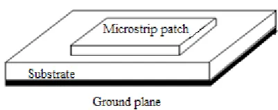
[image:1.595.325.526.230.310.2]The structure of Microstrip antenna is usually consists of a pair of parallel conducting layers separating a dielectric medium, referred to as substrate, as shown in Figure 1. This substrate usually has dielectric constant εr, which is ranging from 2.2 to 12, operating at frequency of 1GHz to 100GHz. In this configuration, the upper conducting layer (patch) is the source of radiation where electromagnetic energy fringes off the edges of the patch and into the substrate, whereas lower conducting layer acts as a perfectly reflecting ground plane,
Figure 1: Typical geometry of a microstrip antenna
bouncing energy back through the substrate and into free space.
2.
ELECTROMAGNETIC BAND GAP
(EBG) STRUCTURE
EBG materials (referred as Metamaterials), are artificial materials engineered to have properties that may not be found in nature [2-3]. Metamaterials usually achieved their properties from structure rather than composition, using small inhomogeneities to create effective macroscopic behavior. The primary research in metamaterials investigates materials with negative refractive index [1]. Main applications of Metamaterials found in the field of remote aerospace applications, sensor detection and infrastructure monitoring, smart solar power management, public safety, radomes, high-frequency battlefield communication and lenses for high-gain antennas, improving ultrasonic sensors, and even shielding structures from earthquakes.
Metamaterial consists of Periodic Structures [2-3]. Electromagnetic metamaterial affects Electro Magnetic waves by having structures in smaller dimension compared to wavelength of light. EBG layers are also called as Frequency Selective Surface (FSS), Artificial Magnetic Conductors (AMC) and High Impedance Surfaces (HIS).The HIS or AMC, is an artificial, metallic, electromagnetic structure. The structure is designed to be selective in supporting surface wave currents, different from conventional metallic conductors. It finds applications in microwave circuits and antennas. Strong surface waves of sufficient strength, which propagate on the metal ground plane will reach the edge and propagated into free space. This creates a multi-path interference. In contrast the HIS suppresses the propagation of surface waves. Furthermore, control of the radio frequency or microwave radiation pattern is efficiently increased, and mutual coupling between antennas is also reduced.
2.1 Negative Refractive Index
materials encountered in optics, such as glass or water, have positive values for both permittivity ε and permeability µ. However, some metals (such as silver and gold) have negative permittivity ε at visible wavelengths. A material having either (but not both) ε or µ negative is opaque to electromagnetic radiation. Although the optical properties of a transparent material are fully specified by the parameters ε and µ, refractive index n is often used in practice, where „n‟ can be determined from:
All known non-metamaterials (transparent materials) possess positive values for ε and µ. By convention the positive square root is used for n. However, some engineered metamaterials have ε < 0 and µ < 0. Because the product of ε and µ is positive, n is real. Under such circumstances, it is necessary to take the negative square root for n. Physicist Victor Veselago proved that such substances can transmit light [11].
Metamaterial with negative n have numerous interesting properties: 1.Snell's law: (n1sinθ1 = n2sinθ2), but as n2 is negative, the rays will be refracted on the same side of the normal on entering the material.
2. The Doppler shift is reversed: that is, a light source moving toward an observer appears to reduce its frequency. 3. The time-averaged Poynting vector: it is antiparallel to phase velocity. This means that unlike a normal right-handed material, the wave fronts are moving in the opposite direction to the flow of energy.
2.2 Types of Metamaterial
There are different types of metamaterials are available and they are classified as follows.
2.2.1 Negative Index Metamaterial:
In Negative Index Metamaterials (NIM), both permittivity and permeability are negative resulting in a negative index of refraction. Hence, because of the double negative parameters these are also known as Double Negative Metamaterials or Double Negative Materials (DNG). Other terminologies used for NIMs are "Left-Handed Media", "Media with a Negative Refractive Index" and "Backward-Wave Media". In optical materials, if both permittivity ε and permeability µ are positive this results in propagation in the forward direction. If both ε and µ are negative, a backward wave is produced. If ε and µ have different polarities, then this does not result in wave propagation.
2.2.2 Single Negative Index Metamaterial
In Single Negative (SNG) metamaterials either permittivity or permeability are negative, but not both. These are Epsilon Negative media (ENG) metamaterials and Mu-Negative media (MNG) metamaterials discussed below. Interesting experiments have been conducted by combining two SNG layers into one metamaterial. These effectively create another form of DNG metamaterial. A slab of ENG material and slab of MNG material have been joined to conduct wave reflection experiments. This resulted in the exhibition of properties such as resonances, anomalous tunneling, transparency, and zero reflection. Like Negative index materials, SNGs are innately dispersive, so their permittivity ε, permeability µ, and refraction index n, will alter with changes in frequency.
2.2.2.1 Epsilon Negative Media (ENG)
In this, permittivity ε is negative while permeability µ is positive. Many plasmas exhibit this characteristic. For
example noble metals such as gold or silver will exhibit this characteristic in the infrared and visible spectrums.
2.2.2.2 Mu-Negative Media (MNG)
In this, permittivity ε is positive while permeability µ is negative. A material, which called Gyrotropic or Gyromagnetic exhibits this characteristic. A Gyrotropic material is a medium that has been altered bythe presence of a Quasistatic magnetic field.
2.3 Little More on Electromagnetic Band
Gap (EBG) Structure
Electromagnetic Band Gap metamaterials control the propagation of light, which is accomplished with either a class of metamaterial known as Photonic Crystals (PC), or another class known as Left-Handed Materials (LHM) [5]. Both are a novel class of artificially engineered structure, and both control and manipulate the propagation of electromagnetic waves. Photonic Crystals can prohibit light propagation altogether. However, both the PC and LHM are capable of allowing it to propagate in certain designed directions. An EBG affects the properties of the photon in the same way the semiconductor materials affect the properties of the electron. So, it happens that the PC is the perfect band gap material, because it allows no propagation of light. Each unit of the prescribed periodic structure acts like large scale atoms. Electromagnetic Band Gap (EBG) structured metamaterials are designed to prevent the propagation of an allocated bandwidth of frequencies, for certain arrival angles and polarizations.
The generation of surface waves decreases the antenna efficiency and degrades the antenna pattern. Furthermore, it increases the mutual coupling of the antenna array. The feature of surface-wave suppression helps to improve antenna‟s performance such as increasing the antenna gain and less power wasted in backward direction propagation. Two types of EBG structure to be tried here. First, without slotted implementation of EBG Layer and second, to find the effect when the patches on the EBG layer are drilled (slotted). EBG structure can be design by various shapes and every shape will have different frequency band gap.
2.4 Surface Wave Current
Surface wave is excited on microstrip antenna when the substrate has dielectric constant єr > 1. Besides end fire radiation, surface wave give rise to coupling between various elements of an array. Surface waves are launched into the substrate at an elevation angle θ which lies between π / 2 and sin-1(1/√ єr). These waves are incident on the ground plane at an angle, get reflected from there, then meet the dielectric-air interface, which again get reflect, following the zigzag path. They finally reach the boundaries of the microstrip structure where they are reflected back and diffracted by the edges giving rise to end-fire radiation.
Figure 2: Propagation of surface waves in substrate of patch antenna
Surface wave propagation is a major problem in Microstrip antennas. Surface waves reduce antenna efficiency and gain, limit bandwidth, increase end-fire radiation, increase cross-polarization levels, and limit the applicable frequency range of microstrip antennas.
Solutions to the surface wave problem are available. One of them is based on the micromachining technology in which part of the substrate beneath the radiating element is etched to realize a low efficiency dielectric constant environment for the antenna. In this case the power loss is reduced and coupling of power to the space wave is enhanced. The other technique relies on Photonics Band Gap (PBG) engineering. We can use EBG structure in many ways. One method is to make the substrate periodically loaded so that the surface wave dispersion diagram presents a forbidden frequency range (stop band or band gap) about the antenna operating frequency. Because the surface waves cannot propagate along the substrate, an increase amount of radiating power couples to the space waves. Another method is that EBG resonator antennas. They are practically useful to enhance the gain of a planar antenna and easy to implement. In these antennas, an EBG material is placed over a metallic ground plane containing a small antenna, to form a resonant cavity, and hence the gain of the small antenna can be enhanced. It is found that the gain of EBG resonator antennas increases with the quality factor Q (Q-factor) of the resonant cavity. Therefore, one of method to further enhance the gain of the EBG antenna is to increase the Q-factor of the resonant cavity. This has been carried out by increasing the number of dielectric EBG layers or using EBG material of high permittivity, but the cost is the increase of the antenna height or the need of expensive materials.
3.
DESIGN OF RECTANGULAR PATCH
AND EBG STRUCTURE
It is required to calculate width and length of the rectangular patch when resonating frequency fo, dielectric constant of the substrate and height of the substrate are given. The design of the rectangular patch is given below.
First step of design is to find width of the patch. For efficient radiation, the width W is given by (1).
Where, C=velocity of light, f0=Resonant frequency, εr= Dielectric constant of the substrate. Given data as
C=3x10⁸m/s, f0=2.4GHz and εr = 4.4 for FR4 results in width of the patch as W=38 mm. The relation between dimensions of the patch along its length which is extended on each end by a distance ΔL and effective dielectric constant εreff, are given by,
Where, W=width of the patch, h=Height of the substrate, and εreff is taken as,
By choosing value of εr=4.4, h=1.57mm and W=38mm we got εreff = 4.09 and hence ΔL= 0.725mm.
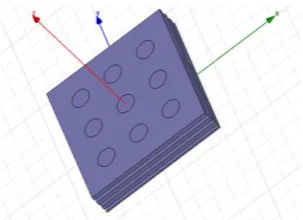
Length of the Patch, L=λ/(2√(εreff))-2ΔL=29.45mm. The effective length of the patch is taken as Leff =L+ 2 ΔL. Thus, the effective length of the patch is Leff =30.9 mm. The patch should maintain (wavelength/2) distance on the substrate i.e. 62.5mm. The Design of EBG Layers is carried out by using patches like Cylindrical, Conical and Cuboidal with and without hole on FSS layer. For the design of Cylindrical Patches on FSS layer we taken Radius=11.032mm, Height=0.1mm, distance between the patches along length of the FSS layer=22.064mm, distance between the patches along width of the FSS layer=23.285mm, height of EBG substrate is taken as 5mm and the distance between the EBG substrate and microstrip patch substrate=5mm. For Cuboidal Patches on FSS layer without hole, we took, Length=22.064mm, Width=23.285mm, Height=0.1mm, distance between the patches along length of the FSS layer=22.064mm, distance between the patches along width of the FSS layer=23.285mm, Height of EBG substrate=5mm, distance between the EBG substrate and microstrip patch substrate=5mm. For Cuboidal Patches on FSS layer with hole, we took, hole Radius1=2.758mm, hole Radius2=5.516mm. And for Conical Patches on FSS layer design, we had Radius=11.032mm, Height1=0.1mm, Height2=1mm, Height3=2mm, Height4=3mm, distance between the patches along length of the FSS layer=22.064mm, distance between the patches along width of the FSS patch substrate=5mm. Layer 1, 2 and 3 for all the three kinds of EBG patches can be used. Figure 3, Figure 4 and Figure 5 show the three kinds of EBG design among 15 EBG structures which we tried and got results for all 15 structures.
[image:3.595.58.279.73.174.2]Figure 3: Designed one layer EBG with FSS consisting of cuboids
[image:3.595.313.540.182.756.2]Figure 5: Three layer EBG with FSS consisting of cones with height 0.1mm
4.
SIMULATION RESULTS
Simulation is carried out successfully at resonating frequency 2.4GHz which is suitable for wireless applications and result is represented in Table.1. Frequencies F1, F2 and Bandwidths are presented respectively in GHz and MHz units. Return Loss and Gains are in dB units. Structures (Str) listed are: Str1-Rectangular patch without EBG, Str2-One layer FSS with cylinders, Str3-One layer FSS with cuboids, Str4-One layer FSS with cones(Height 0.1mm), Str5-One layer FSS with cones(Height 1mm), Str6-One layer FSS with cones(Height 2mm), Str7-One layer FSS with cones(Height 3mm), Str8-One layer FSS with slotted(2.758mm hole) cylinders, Str9-One layer FSS with slotted(2.758mm hole) cuboids, Str10-One layer FSS with slotted(5.516mm hole) cuboids, Str11-Two layers FSS with cylinders(Resonant cavity Height 2.5mm), Str12-Two layers FSS with cylinders(Resonant cavity Height 10mm), Str13-Two layers FSS with cuboids (Resonant cavity height is 5mm), Str14-Three layers FSS with cylinders(Resonant cavity height 1mm), Str15-Three layers FSS with cones with height 0.1mm. Few Simulation results are shown in figure 6 to figure 16. Hence, it is realized that antenna without EBG provides gain of 2.83dB and bandwidth of 60MHz with VSWR of 1.1. After placing different number of EBG layer with different shapes over rectangular patch, we have obtained wide range of results. After comparing the simulation results, we conclude that the best obtained result is with respect to two layers FSS with cylinders having resonant cavity height of 10mm. With this structure we btained gain of 4.51dB at bandwidth of 67.5MHz and VSWR of 1.38.
5.
CONCLUSIONS
The simulated results of various Electromagnetic Band Gap structure at a frequency of 2.4 GHz have been presented. The utilization of the software tool HFSS (High Frequency Structure Simulator) involved in the design process helps to minimize the processing time for the calculation and the simulation of the structures. Many types of EBG structures with different number of layers have been implemented and compared their properties with each other. Integration of the EBG structure with the Microstrip array antenna improved the bandwidth and the gain. By using the EBG structure, the surface wave effect is reduced resulting to the improvement of the antenna performance. As an overall conclusion, all the planned works and the objectives of this paper have been successfully implemented and the improvement of the antenna properties such as bandwidth, gain is compared each other after designing EBG structures.
6.
FUTURE WORK
Further works can be carried out to improve the performance of the EBG structure. Some suggestions for future work are (a) the multi band gap frequency characteristic for EBG structure should be designed to cover the multiband antenna, (b) miniaturized the EBG structure to achieve the compactness of the antenna design, (c) other application of EBG especially in the filter design is carried out, (d) different structure of EBG aiming to reduce the return loss is analysed.
Figure 6: Gain plot for a rectangular patch without EBG
Figure.7: Gain plot for a one layer EBG with FSS consisting of cuboids
[image:4.595.320.529.144.751.2]Figure 8: Gain plot for a two layer EBG with FSS consisting of slotted cylinder
Table 1. SIMULATION RESULTS
1.00 1.50 2.00 2.50 3.00 3.50 4.00
Freq [GHz] -20.00
-15.00 -10.00 -5.00 0.00
d
B(S
(W
a
ve
Po
rt
1
,W
a
ve
Po
rt
1
))
Ansoft Corporation
XY Plot 3
HFSSDesign1m1 m2
m3
Curve Info dB(S(WavePort1,WavePort1)) Setup1 : Sw eep1
Name X Y
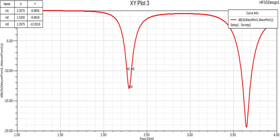
m1 2.2675 -9.9855 m2 2.3200 -9.9919 m3 2.2975 -12.9319
Figure 10: Return Loss versus Frequency plot for a one layer EBG with FSS consisting of Cuboids Sl.
No. Structure
F1 (GHz)
F2 (GHz)
Band Width (MHz)
Return loss
Gain
(dB) VSWR
1 Rectangular Patch without EBG 2.2975 2.3575 60 -28.6 2.83 1.1
2 One layer FSS with cylinders 2.2675 2.32 52.5 -12.93 5.22 1.6
3 One layer FSS with cuboids 2.2675 2.2975 30 -10.317 4.75 1.84
4 One layer FSS with cones (Height 0.1mm) 2.2675 2.32 52.5 -12.98 5.30 1.6
5 One layer FSS with cones (Height 1mm) 2.2675 2.32 52.5 -12.94 5.20 1.57
6 One layer FSS with cones (Height 2mm) 2.2675 2.32 52.5 -12.88 5.20 1.64
7 One layer FSS with cones (Height 3mm) 2.2675 2.32 52.5 -12.88 5.13 1.6
[image:5.595.57.549.373.618.2]1.00 1.50 2.00 2.50 3.00 3.50 4.00 Freq [GHz]
-35.00 -30.00 -25.00 -20.00 -15.00 -10.00 -5.00 0.00
d
B(S
(W
a
ve
Po
rt
1
,W
a
ve
Po
rt
1
))
Ansoft Corporation XY Plot 2 HFSSDesign1
[image:6.595.55.550.71.281.2]Curve Info dB(S(WavePort1,WavePort1)) Setup1 : Sw eep1
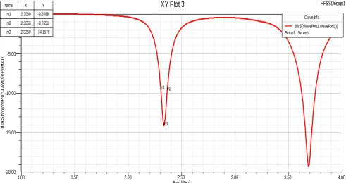
Figure 11: Return Loss versus Frequency plot for two layers EBG with FSS consisting of slotted cylinders
1.00 1.50 2.00 2.50 3.00 3.50 4.00
Freq [GHz] -20.00
-15.00 -10.00 -5.00 0.00
d
B(S
(W
a
ve
Po
rt
1
,W
a
ve
Po
rt
1
))
Ansoft Corporation
XY Plot 3
HFSSDesign1m1 m2
m3
Curve Info
dB(S(WavePort1,WavePort1)) Setup1 : Sw eep1
Name X Y
m1 2.3050 -9.5586
m2 2.3650 -9.7651
m3 2.3350 -14.1578
[image:6.595.57.549.338.598.2]Figure 13: VSWR versus Frequency for a rectangular patch without EBG
1.00 1.50 2.00 2.50 3.00 3.50 4.00
Freq [GHz] 0.00
50.00 100.00 150.00 200.00 250.00 300.00 350.00 400.00 450.00
VS
W
R
(W
a
ve
Po
rt
1
)
Ansoft Corporation XY Plot 4 HFSSDesign1
Curve Info
[image:7.595.56.540.297.504.2]VSWR(WavePort1) Setup1 : Sw eep1
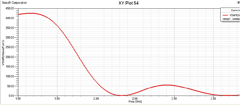
Figure 14: Frequency versus VSWRplot for a one layer EBG With FSS consisting of Cuboids
1.00 1.50 2.00 2.50 3.00 3.50 4.00
Freq [GHz] 0.00
50.00 100.00 150.00 200.00 250.00 300.00 350.00 400.00 450.00
VS
W
R
(W
a
ve
Po
rt
1
)
Ansoft Corporation XY Plot 3 HFSSDesign1
Curve Info
[image:7.595.57.558.537.726.2]VSWR(WavePort1) Setup1 : Sw eep1
1.00 1.50 2.00 2.50 3.00 3.50 4.00 Freq [GHz]
0.00 500.00 1000.00 1500.00 2000.00 2500.00 3000.00 3500.00 4000.00 4500.00
VS
W
R
(W
a
ve
Po
rt
1
)
Ansoft Corporation XY Plot 4 HFSSDesign1
[image:8.595.55.550.74.287.2]Curve Info VSWR(WavePort1) Setup1 : Sw eep1
Figure 16: Frequency versus VSWR plot for three layer EBG with FSS consisting of cones with hieght 0.1 mm
7. REFERENCES
[1] Rongguo Zhou, Hualiang Zhang, Hao Xin, “Metallic Wire Array as Low-Effective Index of Refraction Medium for Directive Antenna Application”, IEEE transactions on antennas and propagation, vol. 58, no. 1, January 2010.
[2] M. Hajj, E. Rodes and T. Monédière, “Dual-Band EBG Sectoral Antenna Using a Single-Layer FSS for UMTS Application”, IEEE Antennas and Wireless Propagation Letter vol. 8, 2009.
[3] Dina Serhal, Mohamad Hajj, Régis Chantalat, Julien Drouet and Bernard Jecko, “Multifed Sectoral EBG Antenna for WiMAX Applications”, IEEE Antennas and Wireless Propagation Letter, vol. 8, 2009.
[4] Yuehe Ge, Karu P. Esselle, and Yang Hao, “Design of Low- Profile High Gain EBG Resonator Antennas Using Genetic Algorithm,” IEEE Antennas and Wireless Propagation Letter, vol. 6, 2007.
[5] Y. Lee, W. Park, J. Yeo and R. Mittra, “Directivity Enhancement of Printed Antennas Using a Class Metamaterial Superstrates”, Electromagn, vol. 26, pp. 203–218, 2006.
[6] S. Wang, A. P. Feresidis, G. Goussetis, and J. C. Vardaxoglou, “High Gain Subwavelength Resonant Cavity Antennas Based on Metamaterial Ground
Planes,” Inst. Elect. Eng. Proc. Microwave Antennas Propagation, vol. 153, no. 1, pp. 1–6, February 2006. [7] N. Guerin, S. Enoch, G. Tayeb, P. Sabouroux, P.Vincent,
and H. Legay, “A Metallic Febry-Perot Directive Antenna”, IEEE Transactions on Antennas Propagation, vol. 54, no. 1, pp. 220–224, January 2006.
[8] A. R. Andrew, K. P. Esselle, B. C. Sanders, and T. S. Bird, “High-Gain 1D EBG Resonator Antenna”, Microwave Opt. Technol. Lett., vol. 47, no.2, pp. 107–114, October 2005.
[9] M. Diblanc, E. Rodes, E. Arnaud, M. Thevenot,T. Monediere, and B. Jecko, “Circularly Polarized Metallic EBG Antenna”, IEEE Microwave Wireless Compon. Lett., pp. 1–3, 2005.
[10] Y. Ge and K. P. Esselle, “GA/FDTD Technique for the Design and Optimization of Periodic Metamaterials”, IET Proc. Microwave Antennas Propagation, Special issue on Metamater, vol. 1, no. 1, pp. 158–164, February1 2000.
[11] C. Balanis: “Antenna Theory Analysis and Design”. [12] Warren L. Stutzman and Gary A. Thiele: “Antenna