International Journal of Emerging Technology and Advanced Engineering
Website: www.ijetae.com (ISSN 2250-2459,ISO 9001:2008 Certified Journal, Volume 4, Issue 5, May 2014)
Implementation of a Non-Isolated, High Gain ZVS/ZCS
DC-DC Converter
S. Kanimozhi
1, Dr. V. Rajini
21
PG Scholar, 2Professor, SSN College of Engineering, Chennai.
Abstract—This paper presents implementations of a non-isolated, high voltage gain DC-DC converter. High voltage gain is achieved due to inclusion of resonance and transformer in the circuit. The performance of this converter is compared with two similar topologies namely coupled inductor-switched capacitor step-up converter and coupled inductor step-up converter. The proposed prototype is designed using a high frequency transformer providing both electrical and magnetic coupling, hence the converter is said to be non-isolated. The transformer provides hybrid switching technique which combines both conventional linear PWM and traditional resonant conversion, so that the converter achieves ZVS turn on of the switch and ZCS turn off of the diodes. The transformer transfers the inductive and capacitive energy simultaneously to increase the voltage gain of the converter and decreases the size of the magnetic component. Also switching losses of the proposed converter is reduced by incorporating the resonant mode, thereby increases the efficiency. The voltage stresses of all the devices are reduced.
Keywords—High frequency transformer (HT), High voltage gain, Non-Isolated DC-DC converter, Zero voltage switching (ZVS), Zero current switching (ZCS).
I. INTRODUCTION
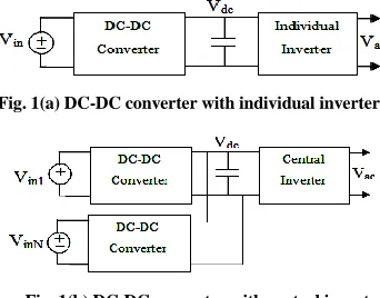
Renewable energy source such as solar energy have increasing in application to reduce carbon footprint. The voltages obtained from solar PV arrays are relatively low value. Therefore, the demand for DC-DC converter with high voltage gain has increased. Power conditioning system (PCS) is required to convert low voltage into high voltage before converting into AC for grid connection as shown in Fig.1[1]. The voltage obtained from PCS should be greater than peak voltage of an inverter generally which is greater than 400V. PCS is designed to provide high voltage gain. The design of PCS can be single stage or double stage. The double stage PCS would reduce ripple at the output of PV array compared to single stage PCS as shown in Fig.1 [1]-[10], PCS have DC-DC converter and DC-AC inverter that will be connected to grid. High voltage gain DC-DC converter can be isolated or isolated [2]-[11], non-isolated tends to be more efficient than non-isolated. In the double stage PCS design, the DC-DC converter would be connected to low power individual inverter or high power centralized inverter as shown in Fig. 1(a) & (b).
Conventional boost converter topologies without transformer cannot provide such high voltage gain. An earlier paper on high voltage gain, non-isolated DC-DC converter [12] employs diode and coupled winding to perform the function of active clamp to achieve high efficiency. However, the voltage stresses across the device are higher than the output voltage.
Fig. 1(a) DC-DC converter with individual inverter
Fig. 1(b) DC-DC converter with central inverter
[image:1.612.359.530.309.443.2]International Journal of Emerging Technology and Advanced Engineering
Website: www.ijetae.com (ISSN 2250-2459,ISO 9001:2008 Certified Journal, Volume 4, Issue 5, May 2014)
II. SYSTEM DESCRIPTION
[image:2.612.73.261.220.422.2]In grid connected system as shown in Fig. 2, there is a need to use a high voltage gain DC-DC converter. The prototype proposed in this work can be used for such applications. Also the prototype has source side application of renewable energy.
Fig.2 Single phase grid connected power system
III. OPERATING PRINCIPLES OF THE PROPOSED
CONVERTER
Fig. 3 Proposed DC-DC converter
The above figure shows the circuit topology of proposed DC-DC converter. This converter consist of transformer, one MOSFET switch, three capacitors and diodes. Here HT is transformer, S1 is the active MOSFET switch. Dc is the
clamping diode, which provides a current path for the leakage inductance of the transformer when S1 is OFF.
Cc is clamping capacitor. Cr is resonant capacitor. Lr is resonant inductor. Dr is resonant diode. WhereCc , Cr , Lr , and Dr forms the resonant part of the circuit. The leakage energy captured by Cc is transformed to Cr through the resonant part of the circuit.Dr provides a unidirectional current flow path for the operation of the resonant portion of the circuit. Cr has resonant charge and linear discharge, and it operates in the hybrid mode. The turn on of D1 is determined by the state of the MOSFET switch S1. Do is the output diode, Co is the output capacitor and Ro is the output resistive load. The voltage across the switches can be clamped and adjusted by the turn’s ratio of the transformer. For this reason, the voltage level of the switch is reduced significantly and low conducting resistance Rds(on) of the switch can be used. Thus, the efficiency of the proposed converter can be increased and high voltage gain can be achieved. To simplify the circuit analysis, the following conditions are assumed.
1) The DC input voltage is stiff and constant. 2) All the switches and diodes are ideal.
There are five distinctive steady state modes for this proposed DC-DC converter.
A. Mode 1:t0-t1
During this mode MOSFET switch S1 is on with ZVS.
When the voltage of the diode across the switch S1 is zero,
S1 turn on. The primary side of transformer is charged by
input voltage Vin, while resonant capacitor Cr is charged by
[image:2.612.370.520.295.386.2]clamping capacitor Cc as shown in Fig 4. Thus both primary input and secondary resonant current flows through the MOSFET switch S1.
Fig. 4 Mode 1
B. Mode 2: t1-t2
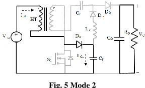
At time t1 MOSFET switch is off. When the MOSFET
switch is turned off, the clamping diode Dc is turned on by stored leakage energy in the transformer. The clamping capacitor Cc is charged by the leakage current as shown in Fig 5. The voltage across the MOSFET switch is clamped by the clamping capacitor. The resonant diode Dr is turn off
[image:2.612.372.516.510.598.2]with ZCS. When the resonant current reaches zero, the resonant diode Dr is turn off.
Fig. 5 Mode 2
C. Mode 3: t2-t3
At time t2 the clamping capacitor is charged to certain
International Journal of Emerging Technology and Advanced Engineering
[image:3.612.361.526.166.420.2]Website: www.ijetae.com (ISSN 2250-2459,ISO 9001:2008 Certified Journal, Volume 4, Issue 5, May 2014)
Fig. 6 Mode 3
D. Mode 4: t3-t4
At time t3 the clamping diode Dc is turned off with ZCS.
When the magnetizing current reaches zero, clamping diode Dc is turn off. While the output diode is still remain in on
state. Hence, inductive and capacitive energy is still transferred to the load as like previous mode as shown in Fig 7.
Fig. 7 Mode 4
E. Mode 5: t4-t0
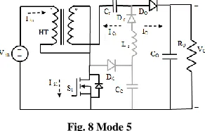
At time t4 the MOSFET switch S1 is turned on with ZVS
due to the leakage energy stored in the transformer. While the output diode still remain in on state for a short time. Hence, output current flows for a short time period. The output diode will be turned on at then the next switching cycle starts again as shown in Fig 8.
Fig. 8 Mode 5
The waveform of five steady state modes for the proposed DC-DC converter is shown in Fig. 9. G1 is the
gating pulse. Iin is the input current. IS1 is the switch current.
Icr resonant capacitor current. Icc is the clamping capacitor
current. IO is the output current. VS1, Vdc, Vdr, Vdo are the
voltage across MOSFET switch, diode Dc, Dr, Do
respectively. The waveform shows the charge in the capacitors must satisfy the charge balance that is when resonant capacitor is charging, the clamping capacitor is discharging.
The current in the resonant capacitor combines resonant charge and linear discharge as shown in the waveform.
Fig. 9 The waveform of five steady state modes
IV. DESIGN PARAMETERS
The proposed converter is designed for duty cycle D=0.5, Resonant inductor Lr = 2.2µH, Resonant capacitor Cr=1µH;
Input voltage Vin =45V. The calculated values of various
[image:3.612.94.241.324.412.2]parameters are shown in Table 1
TABLE I Calculation Of Design Parameters
Parameters Formulae Values
Voltage gain
16
Switching frequency √
88kHz
Voltage stress across
switches Vs1 &VDc
60V
Voltage stress across
diodes VDr &VD0
( )
340V
ILm_sec is average linear magnetizing current referred to secondary side of the HT
0.275A
Average input current Iin
( ) ( )
23.06A
Resonant contribution
index
[image:3.612.96.242.513.606.2]International Journal of Emerging Technology and Advanced Engineering
Website: www.ijetae.com (ISSN 2250-2459,ISO 9001:2008 Certified Journal, Volume 4, Issue 5, May 2014)
V. SIMULATION RESULTS OF PROPOSED CONVERTER
[image:4.612.383.520.135.206.2]The proposed converter is simulated in MATLAB. Fig 10 shows the output voltage with ripple of 0.6586%. The switching frequency 88 kHz is used to trigger the MOSFET switch.
Fig.10 Output voltage of the proposed converter
[image:4.612.89.246.202.285.2]The voltage across switch and diodes are clamped as shown in the Fig. 11 for 45 Volts input. The simulation result of voltages across the switch and diodes are shown in below figure.
Fig. 11 Voltage across switch and diodes
VI. RESULTS AND DISCUSSIONS
Efficiency of proposed converter for various duty ratios is represented in figure 12.
Fig. 12 Plot between duty cycle and efficiency
From the Fig 12, it is clear that the efficiency of the proposed converter is maximum at 0.5 duty ratio. For the proposed converter the effect of output voltage for different input voltage is represented in figure 13. Here, duty ratio of 0.5 and switching frequency of 88 kHz has been used.
Fig. 13 Plot between input voltage and output voltage
From the Fig 13, it is clear that the output voltage is increasing with the input voltage. For the proposed converter the effect of output voltage for different load is represented in figure 14. Here, duty ratio of 0.5 and switching frequency of 88 kHz has been used.
Fig. 14 Plot between resistive load and output voltage
From the Fig 14, it is clear that the output voltage is in the range of 400V-500V.
VII. COMPARISON WITH NON-RESONANT CONVERTERS
The proposed high voltage gain converter is compared with coupled inductor converter and coupled inductor-switched capacitor converter. The boost converter output terminal and flyback converter output terminal are serially connected to increase the output voltage gain in the coupled inductor as shown in Fig 15 is proposed by [13], [14]. By adding a switched capacitor in series with the energy transformer path, a new improved high boost ratio dc–dc converter with coupled inductor-switched capacitor, as shown in Fig 16 is proposed by [15].
[image:4.612.371.512.291.369.2] [image:4.612.100.238.363.432.2] [image:4.612.106.243.504.578.2]
International Journal of Emerging Technology and Advanced Engineering
Website: www.ijetae.com (ISSN 2250-2459,ISO 9001:2008 Certified Journal, Volume 4, Issue 5, May 2014)
[image:5.612.336.561.117.268.2]
Fig. 16 Coupled inductor-Switched capacitor converter
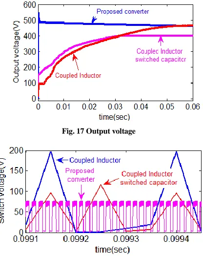
For the input voltage of 45 Volts, voltage gain of 10, duty ratio of 0.5 and switching frequency of 88 kHz, the coupled inductor-switched capacitor converter is simulated in MATLAB. Simulated output voltage waveform is shown in Fig 17. Voltage across switch and diodes are shown in Fig 18, Fig 19, Fig 20.
[image:5.612.85.264.134.217.2]
Fig. 17 Output voltage
Fig. 18 Voltage across switch
Fig. 19 Voltage across output diode
A. Comparison of Component size and Efficiency
The various component of proposed converter is compared with coupled inductor-switched capacitor for voltage gain of 10, switching frequency of 88 kHz and duty ratio of 0.5 duty ratio as shown in Table II. Also the efficiency of proposed converter is compared with non-resonant converters in terms of switching losses, switching stresses as shown in Table III.
TABLEII
COMPARISON OF COMPONENT SIZE OF PROPOSED AND NON -RESONANT CONVERTERS
Component Coupled Inductor
Coupled Inductor- Switched Capacitor
Proposed Converter Leakage inductor Llk 0.7µH 7 µH —
Resonant inductor Lr — — 2.2 µH
Resonant capacitor Cr — — 1µF
Clamp capacitor Cc 200µF 300 µF 20µF Output capacitor Co 2000µF 300 µF 2.2µF
Charge capacitor Cs — 300 µF —
Transformer coupling coefficient Lm
[image:5.612.67.275.312.574.2]International Journal of Emerging Technology and Advanced Engineering
Website: www.ijetae.com (ISSN 2250-2459,ISO 9001:2008 Certified Journal, Volume 4, Issue 5, May 2014)
TABLEIII
COMPARISON OF EFFICIENCY OF PROPOSED AND NON-RESONANT
CONVERTERS
The above tabulations show that the component size and efficiency of the proposed converter is more than the coupled inductor and coupled inductor-switched capacitor converters.
VIII. EXPERIMENT VERIFICATIONS
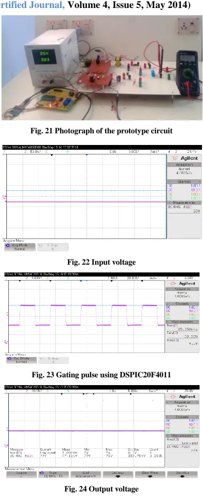
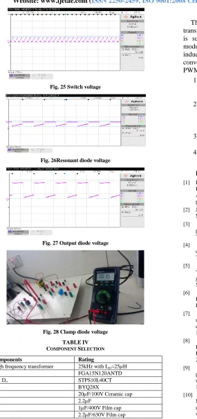
The below figures shows the hardware result of prototype with 25 volts inputs, 25 kHz of switching frequency with 50% on time.
Fig. 21 Photograph of the prototype circuit
[image:6.612.341.547.120.626.2]Fig. 22 Input voltage
Fig. 23 Gating pulse using DSPIC20F4011
Fig. 24 Output voltage Component Parameter Coupled
inductor
Coupled inductor-Switched capacitor
Proposed converter
MOSFET Switch
Switch voltage
126.5V 90V 65V
Conduction losses
180.54W 174.41W 47.78W
Switching losses
15.98W 14.91W 4.79W
Clamp diode Dc Diode voltage
234.7V 88.27W 43.98V
Conduction losses
0.0311W 0.0231W 0.001W
Switching losses
4.795W 3.598W 0.7992W
Output diode Do
Diode voltage
553.9V 402.5W 251.6V
Conduction losses
0.0094W 0.0231W 0.00042W
Switching losses
1.598W 1.598W 1.598W
Resonant diode Dr
Diode voltage
— — 487.7V
Conduction losses
— — 0.00682W
Switching losses
— — 0.7992W
Charge Diode Ds
Diode voltage
— — 88.27W
Conduction losses
— — 0.0217W
Switching losses
— — 1.598W
Transformer Conduction losses
0.132W 0.109W 0.00000258W
Switching losses
0.00000148 W
0.00625 W
0.00000154W
[image:6.612.44.304.159.552.2]International Journal of Emerging Technology and Advanced Engineering
[image:7.612.59.344.124.731.2]Website: www.ijetae.com (ISSN 2250-2459,ISO 9001:2008 Certified Journal, Volume 4, Issue 5, May 2014)
Fig. 25 Switch voltage
Fig. 26Resonant diode voltage
Fig. 27 Output diode voltage
Fig. 28 Clamp diode voltage
TABLEIV COMPONENT SELECTION
Components Rating
High frequency transformer 25kHz with Lm=25µH
S1 FGA15N120ANTD
Dr , Do STPS10L40CT
Dc BYQ28X
Cc 20µF/100V Ceramic cap
Lr 2.2µF
Cr 1µF/400V Film cap
Co 2.2µF/630V Film cap
IX. CONCLUSION
The proposed high voltage gain DC-DC converter with transformer which combines both resonant and linear mode is suitable for low input voltage such as photovoltaic module. The proposed converter is compared with coupled inductor and coupled inductor-switched capacitor converters. The resonant mode incorporated into the linear PWM converter has the following advantages
1) When the switch is off both the inductive and capacitive energy is simultaneously transferred into load thus increases the voltage gain.
2) The conduction and switching losses are reduced as compared with the coupled with the coupled inductor-switched capacitor. Hence, efficiency is increased for the proposed converter.
3) Voltage stress across the switch and diodes are reduced.
4) Size of the magnetic component with hybrid transformer is well suited for high gain applications.
REFERENCES
[1] B.Gu, J.Dominic, J.S.Lai, Z.Zhao, C.Liu, ―High Boost Ratio Hybrid Transformer DC-DC Converter for Photovoltaic Module Applications‖ IEEE Trans. Power Electron., vol. 28, NO. 4, pp.2048-2058, Apr.2013.
[2] J.S.Lai, ―Power conditioning circuit topologies,‖ IEEE Ind. Electron. Mag., vol. 3, pp. 24-34. Jun. 2009.
[3] S. B. Kjaer, J. K. Pedersen, and F. Blaabjerg, ―A review of single phasegrid-connected inverters for photovoltaic modules,‖ IEEE Trans. Ind. Appl., vol. 41, no. 5, pp. 1292–1306, Sep./Oct. 2005. [4] F. Blaabjerg, Z. Chen, and S. B. Kjaer, ―Power electronics as
efficient interface in dispersed power generation systems,‖ IEEE Trans. Power Electron., vol. 19, no. 5, pp. 1184–1194, Sep. 2004. [5] Y. Xue, L. Chang, S. B. Kjaer, J. Bordonau, and T. Shimizu,
―Topologies of single-phase inverter for small distributed power generators: An overview,‖ IEEE Trans. Power Electron., vol. 19, no. 5, pp. 1305–1314, Sep. 2004.
[6] B. Liu and S. Duan, ―Photovoltaic DC-building-module-based BIPV system-concept and design considerations,‖ IEEE Trans. Power Electron., vol. 26, no. 5, pp. 1418–1429, May 2011. [7] Q. Li and P.Wolfs, ―A review of the single phase photovoltaic
module integrated converter topologies with three different DC link configurations,‖ IEEE Trans. Ind. Electron., vol. 23, no. 23, pp. 1320–1333, Apr. 2008.
[8] W. H. Li and X. N. He, ―Review of non-isolated high step-up DC/DC converters in photovoltaic grid-connected applications,‖ IEEE Trans. Ind. Electron., vol. 58, no. 4, pp. 1239–1250, Apr. 2011.
[9] R. J.Wai, C. Y. Lin, R. Y. Duan, and Y. R. Chang, ―High-efficiency power conversion system for kilowatt-level stand-alone generation unit with low input voltage,‖ IEEE Trans. Ind. Electron., vol. 55, no. 10, pp. 3702–3714, Oct. 2008.
International Journal of Emerging Technology and Advanced Engineering
Website: www.ijetae.com (ISSN 2250-2459,ISO 9001:2008 Certified Journal, Volume 4, Issue 5, May 2014) [11] W. Yu, J. S. Lai, H. Qian, and C. Hutchens ,―High Efficiency
MOSFET Inverter with H6-Type Configuration for Photovoltaic Non-isolated AC-Module Applications‖ IEEE Trans. Power Electron., vol. 56, no. 4, pp. 1253-1260, Apr. 2011
[12] Q. Zhao and F. C. Lee, ―High-efficiency, high step-up dc–dc converters,‖IEEE Trans. Power Electron., vol. 18, no. 1, pp. 65–73, Jan. 2003.
[13] K. C. Tseng and T. J. Liang, ―Novel high-efficiency step-up converter,‖ Proc. Inst. Elect. Eng.—Elect. Power Appl., vol. 151, no. 2, pp. 182–190, Mar. 2004.
[14] T. J. Liang and K. C. Tseng, ―Analysis of integrated boost-flyback step-up converter,‖ proc. Inst. Elect. Eng.-Electr: Power Appl., vol. 152, no. 2, pp. 217–225, Mar. 2005.
[15] R. J.Wai and R. Y. Duan, ―High step-up converter with coupled-inductor,‖ IEEE Trans. Power Electron., vol. 20, no.5, pp. 1025– 1035, Sep. 2005.
[16] R. J. Wai, C. Y. Lin, R. Y. Duan, and Y. R. Chang,―High-efficiency DC–DC converter with high voltage gain and reduced switch stress,‖ IEEE Trans. Ind. Electron., vol. 54, no. 1, pp. 354–364, Feb. 2007. [17] M. Orudente, L. L. Pfitscher, H. Emmendoerfer, E. F. Romaneli,
and R. Gules, ―Voltage multiplier cells applied to non-isolated DC-DC converters,‖ IEEE Trans. Power Electron., vol. 23, no. 2, pp. 871–887, Mar.2008.
[18] H. Ye and F. L. Luo, ―Positive output super-lift converters,‖ IEEE Trans.Power Electron., vol. 18, no. 1, pp. 105–113, Jan. 2003. [19] E. H. Ismail, M. A. Al-Saffar, A. J. Sabzali, and A. A. Fardoun, ―A
family of single-switch PWM converters with high step-up conversion ratio,‖ IEEE Trans. Circuit Syst. I, vol. 55, no. 4, pp. 1159–1171, May 2008.
[20] B. Axelrod, Y. Berkovich, and A. Ioinovici, ―Transformerless DC– DC converters with a very high DC line-to-load voltage ratio,‖ in Proc. IEEE Int. Symp. Circuits Syst. (ISCAS), 2003, pp. III435– III438.
BIOGRAPHY
Dr. V. Rajini, Professor in the department of Electrical and Electronics Engineering, SSN college of Engineering, has 18 years of teaching and research experience including 4 years of research experience in polymeric insulating materials in Anna University. She received her BE and M.E( University Rank1) degrees in Electrical Engineering from Annamalai University and Ph.D in High Voltage Engineering from Anna University. She has published over 35 research publications in referred journals and international conferences. She is currently working on the development of novel cable insulating materials for nuclear power plants. She is a member of IEEE and Life member of ISTE.
S. Kanimozhi, M.E (Power Electronics & drives) student in the department of Electrical and
Electronics Engineering, SSN college of
Engineering. She is currently doing her project work on non-isolated DC-DC converter using
hybrid transformer with the guidance of