Abstract- The study of a planar G-band extended interaction oscillator (EIO) driven by a pseudospark-sourced sheet electron beam is presented. This enables the advantages of a planar interaction circuit combined with the merits of a pseudospark-sourced sheet electron beam including large beam cross section, high current density and the fact that a pseudospark-sourced electron beam does not require the use of an external focusing magnetic field. Beam-wave interaction simulations for this planar EIO predicted a peak output power of 2.1 kW at around 0.2 THz. Investigations indicate that this planar EIO has a better tube performance with a higher radiation power compared with the pseudospark-sourced pencil electron beam EIO.
Index Terms— Extended interaction oscillator, sheet electron beam, pseudospark-sourced electron beam, sub-terahertz, high power radiation.
I. INTRODUCTION
n the millimeter-wave and terahertz (THz) community, high power radiation sources have many potential applications including high data rate communications, security threat detection, high resolution imaging, and biological spectroscopy and biomedical diagnostics [1-2]. Vacuum electron devices (VEDs) have been widely studied to realize many of these applications operating in the so-called THz gap [3-9]. Among various VEDs, the EIO has gained considerable attention as a promising THz oscillation source to satisfy some of these applications, due to its high gain per unit length and compact configuration [4-9]. In the design, we use a pseudospark-sourced (PS) electron beam instead of the conventional electron beam produced by a thermionic cathode to drive the EIO to achieve devices that are more compact. There are many advantages regarding the PS electron beam, including high beam current density, simple structure for easier fabrication, low vacuum requirement and its propagation with no need of any external focusing magnetic field [10-15]. The PS electron beam has been extensively studied, and widely applied to generate millimeter-wave and THz radiation at the University of Strathclyde, including a 0.2 THz backward wave
Manuscript received XX. This work is supported by the U.K. Engineering and Physical Sciences Research Council (EPSRC).
G. X. Shu is with the School of Physical Electronics, University of Electronic Science and Technology of China, Chengdu, 610054 China, and also with the Department of Physics, University of Strathclyde, Glasgow G4 0NG, U.K. (e-mail: [email protected]).
W. He, L. Zhang, H. Yin, J. P Zhao A. W. Cross, and A. D. R. Phelps are with the Department of Physics, University of Strathclyde, Glasgow G4 0NG, U.K. (e-mail: [email protected]; [email protected]; [email protected]; [email protected];[email protected]).
oscillator (BWO) with a tested output power of 20 W [14], a Ka-band Cherenkov maser with a ~2 kW measured peak power [15], and a W-band EIO with a tested peak power of 38 W [5]. As the generation and propagation of a high current electron beam will become more challenging for higher frequency VEDs, the advantages of a PS electron beam mentioned above become more attractive at higher frequencies. However, the output power will be subject to a large reduction as the frequency increases, due to the greatly increased loss in the copper circuits and the reduced beam power. To alleviate such a fall-off in power, a sheet electron beam where the beam is extended in one dimension is extremely attractive [16-22]. However, despite the attractive properties in sheet beam vacuum electronics technology, development of a THz sheet beam device with a thermionic cathode is still challenging. One of the key issues is that it is challenging to transport the sheet electron beam with conventional focusing approaches, either with a permanent magnet or with a solenoid. The pseudospark discharge system can address this issue by the ion channel generated in the discharge process used to guide the electron beam.
The measured output power of the pseudospark-sourced pencil electron beam (PS-PEB) W-band EIO is much less than its prediction [5]. Initial analysis demonstrates that it is mainly caused by beam current loss in the circuit and large beam velocity spread. In this paper, improvements are made to alleviate the disadvantageous effects from these two factors. We propose to combine the advantages of large beam cross section in a sheet electron beam and high beam current density in a PS electron beam, aiming to achieve a compact sub-THz EIO with high output power. To verify this idea, a G-band pseudospark-sourced sheet electron beam (PS-SEB) EIO was designed and studied. To see if this EIO has achieved better tube performance, a comparison is made between the sheet and pencil electron beam EIOs based on the pseudospark discharge. The paper is organized as follows: section II gives an introduction of the PS-SEB. Section III presents the design of a PS-SEB EIO, including the cold cavity analysis and 3D beam-wave interaction simulations. Comparisons in tube performance between the PS-SEB and PS-PEB EIOs are made in section IV. A brief conclusion is given in section V.
II. INTRODUCTION OF THE PS-SEB
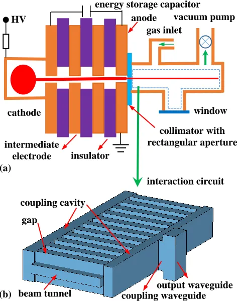
As shown in Fig. 1(a), the EIO consists of a pseudosaprk discharge system and an interaction circuit. The pseudospark discharge system is composed of a cathode with a cylindrical hollow cavity, several intermediate electrodes, several insulators and a planar anode. When the anode is grounded and
Study of a 0.2 THz extended interaction oscillator
driven by a pseudospark-sourced sheet electron
beam
Guoxiang Shu, Wenlong He, Liang Zhang, Huabi Yin, Junping Zhao, Adrian W. Cross,
and Alan D.R. Phelps
the hollow cathode is applied with a negative high voltage, the pseudospark discharge will occur if the pressure in the system is suitably low (typically 6.5–65 Pa). During the pseudospark discharge process, electron beams with very high current can be produced. A PS electron beam with a current of 240 A was measured [11]. The beam current density can reach more than 108 A/m2 [10, 14]. When the beam propagates through the anode and the interaction circuit, its front edge ionizes the background gas and generates a plasma channel. The following beam electrons will expel part of the plasma electrons while the much heavier ions remain fixed. Thus, a positive ion channel is formed to focus the PS electron beam. Due to the extremely high beam current density, a relatively high beam current can still be achieved even while suffering from a high electron beam interception. 15% of the PS electron beam (about 36 A) has been experimentally measured to propagate through a 90-mm-long and 3.5-mm-diameter collimator [11]. A beam current for a 0.07-mm-diameter micro beam was also measured at 20 cm downstream of the anode [14].
Fig. 1 (a) EIO composed of the pseudospark discharge system and the interaction circuit. (b) Interaction circuit composed of a resonant slow wave structure (SWS) and an output structure.
Unlike the more common sheet electron beam produced by a thermionic cathode, an external electric field is not required to compress the beam’s narrow side in the formation of the PS-SEB, a PS-SEB with high current density can be directly achieved using a collimator with a rectangular aperture placed at the end of the anode. The collimator’s rectangular aperture should be located in the same axial center as the anode’s cylindrical aperture, but with a smaller cross section size. In a sheet electron beam that uses a thermionic cathode, the required
focusing force provided by the external magnetic field is much higher along the narrow side than the wide side, thus greatly increasing the focusing difficulty. Such a situation does not exist in a PS-SEB. Like the PS-PEB, the PS-SEB is also focused by the positive ion channel.
III. DESIGN AND SIMULATION OF A PS-SEBEIO
As shown in Fig. 1 (b), the interaction circuit is composed of a resonant SWS and an output structure. The ladder-based SWS used in the design consists of a beam tunnel, eleven gaps, and two coupling cavities. When a short circuit plane is placed at the front and back end of the structure respectively, a resonant SWS is formed. The generated electromagnetic (EM) wave in the resonant SWS is extracted through an output structure. Based on the similar ladder-based SWS [7, 16-17], some changes were made to achieve a relatively easy-to-fabricate configuration, at the cost of tube performances. The beam tunnel directly connects with the coupling cavities at its two sides, without slot waveguides [7, 16] or dumbbell shaped waveguides [17] between the beam tunnel and coupling cavities. The resonant SWS connects to the standard output waveguide through one coupling waveguide, rather than two symmetrical coupling waveguides at its two sides [17].
A. Cold cavity analysis and design of the interaction circuit
The period d of the SWS can be initially set using the synchronous condition of the EIO
( 1, 2,3...)
2 e
N
d T N
v (1) where T is the period of the EM wave. N is a constant related to the operating mode. To achieve an efficient beam-wave interaction, the SWS should operate in a resonant status. When
N equals 1 and 2, it corresponds to the phase difference θ=Kzd
(Kz is the axial propagation constant) of π and 2π, respectively.
5 2
1 (1 / 5.11 10 )
e
v U c is the velocity of the electron beam, decided by the operating voltage U and c is the velocity of light in vacuum. As the required power level for the power supply is actually low due to the pulse operation mode, a compact power supply can be achieved by a step-up pulse transformer with capacitors as energy storage components. A small U is obviously beneficial, and it can be achieved by decreasing d, however it will inevitably increase the fabrication difficulty. Thus, a tradeoff should be made. Initially, N was chosen as 2, and d was set at 0.48 mm, corresponding to a moderate U of 28.5 kV.
CST Microwave Studio was used to analyze and optimize the SWS. The conductivity of the background material is set as
σCu/3 (σCu=5.8×10⁷ S/m). As shown in Fig. 2(a) (inset), a
TM11-like mode was chosen as the operating mode of the one-period SWS as the longitudinal electric Ez field is the cause
of the beam-wave interaction. The coupling impedance Kc
appears to become infinite when the phase difference is π or 2π, and it will decrease when moving away from these two points. As the oscillation current is inversely proportional to Kc, the
EIO will become more difficult to oscillate with a decreased Kc. Thus, oscillation may only occur around the π or 2π region, resulting in an effective oscillating voltage region. As the interaction circuit
cathode HV
insulator
anode
collimator with rectangular aperture gas inlet
vacuum pump
window
intermediate electrode
energy storage capacitor
(a)
(b) beam tunnel coupling waveguide output waveguide coupling cavity
[image:2.612.54.293.280.580.2]voltage of a PS electron beam will gradually reduce with the discharge time, a wider oscillating voltage region is expected to achieve an effective beam-wave interaction over a longer time. The one-period SWS is optimized to obtain the following aspects. (1) A weak dispersion characteristic (the change rate of the phase velocity versus frequency is small) to achieve a wide oscillating voltage region. (2) A large Kc to enhance the
beam-wave interaction. (3) Large beam tunnel to allow more electrons to be transported through the circuit. (4) Small frequency interval between the operating mode and the closest competing mode (TM31-like mode). The coupling impedance characteristic and dispersive curve of the optimized SWS are respectively demonstrated in Fig. 2(a) and (b).
Fig. 2 Simulation results for the one-period SWS. (a) Coupling impedance and (b) dispersion curves. The inset gives the Ez-field
distribution.
A TM110-like 2π resonant mode is chosen as the operating mode of the interaction circuit as the 2π mode has the same
Ez-field direction at each gap. Hence, the modulation of the
electron beam tends to accumulate, contributing to an enhanced beam bunching and thus a higher gain per unit length. Good performance is achieved from the optimized interaction circuit, including (1) good Ez-field uniformity across both the z-axis
and x-axis direction, as shown in Fig.3 (a), contributing to the
high interaction efficiency. (2) A high R/Q of 890 for the operating mode, as shown in Fig. 3 (b), contributes to an enhanced beam-wave interaction. (3) A high Q0 of 1100
contributing to fast oscillation. (4) A small Qe of 197.3, which is beneficial for extracting high power from the cavity. (5) A relatively short circuit length of 5.55mm, which is beneficial for the beam propagation and reduces the disadvantageous effect from the copper loss.
Fig. 3 Simulation results for the interaction circuit. (a) Ez-field
magnitude versus z-axis. (b) R/Q for different modes.
B.Beam-wave interaction simulations and analysis
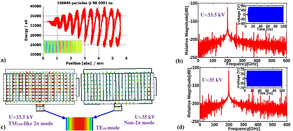
[image:3.612.315.569.150.252.2]For a simple evaluation of the EIO properties, a CW sheet electron beam was used in PIC simulations by CST Particle Studio. From the dispersive curve depicted in Fig. 2(b), the 28.5 kV beam line intersects the operating mode around 2π. As the beam-wave interaction is very intensive in the RSWS, a higher voltage of 33.5 kV was used in the simulation to ensure most of the beam electrons convert their energy to the EM wave, rather than absorbing energy from the resonant field. Based on the experimental results regarding the PS electron beams (A >108 A/m2 beam current density can be achieved), a beam current of 1.7A is injected into the interaction circuit, already having taken into account the loss of electrons due to a high
Fig. 4 CST Particle Studio simulation results. (a) Phase space plots of electrons at the end of the circuit and the inset gives the trajectory of electrons. (b) Output voltage signal (inset) and the corresponding frequency spectrum when U is 33.5 kV. (c) Ez-field distribution when U is
33.5kV (left-top) and 35kV (right-top), and the E-field distribution at the output port (below). (d) Output voltage signal (inset) and the corresponding frequency spectrum when U is 35 kV.
1 1.2 1.4 1.6 1.8 22
0 0.5 1 1.5
2x 10
4
kzd/π
C
o
u
p
li
n
g
i
m
p
e
d
a
n
c
e
[O
h
m
]
The operating mode
(a) (b) 1 1.5 2 2.5 3
190 195 200 205 210 215
kzd /π
F
re
q
u
e
n
c
y
[G
H
z]
U=28.5 kV The operating mode
10 20 30 40 50
0 150 300 450 600 750 900
Mode Number
R
/Q
(a)0 1 2 3 4 5 5.55 (b)
2 4 6 8
10x 10
9
Z [mm]
M
a
g
(E
z)
x=0 mm y=0 mm x=0.5 mm y=0 mm x=-0.5 mm y=0 mm
0 100 200 300 400 500 600
-250 -200 -150 -100
Frequency[GHz]
R
e
la
ti
v
e
M
a
g
n
it
u
d
e
[d
B
]
0 100 200 300 400 500 600
-250 -200 -150 -100
Frequency[GHz]
R
e
la
ti
v
e
M
a
g
n
it
u
d
e
[d
B
]
(a) (b)
TE10 mode
(c) (d)
0 20 40 60 80 100
-90 -45 0 45 90
Time [ns]
V
o
lt
a
g
e
[
V
]
0 20 40 60 80 100
-70 -35 0 35 70
Time [ns]
V
o
lt
a
g
e
[
V
]
U=33.5 kV
U=35 kV
U=35 kV
U=33.5 kV
[image:3.612.48.297.209.313.2] [image:3.612.62.555.461.681.2]interception rate. In addition, a constant axial magnetic field of 1.5 T was used in the simulation.
When the electron beam is injected into the interaction circuit, the EM wave tends to be excited. Electron beam modulation, bunching and energy exchange will take place in the resonant SWS. The generated EM wave can be extracted from the standard output waveguide. As shown in Fig. 4(a), obvious beam electron bunching and energy conversion are observed, implying effective beam-wave interaction. As shown in Fig. 4(b) (inset), a stable time-correlated output signal of 100 ns duration with 74.1 V, which corresponds to an output power of 2.8 kW, is observed at the output port. The oscillation startup time Ts (the time required to reach 0.5 V for the output signal) is
about 5.1 ns. It is expected to be as small as possible to achieve a rapid oscillation. It can also be seen that a clean frequency spectrum was obtained with an obvious peak at 199.95 GHz, which is in good agreement with the achieved frequency in cold cavity analysis (200 GHz). Compared with the peak at 199.95 GHz, the relative magnitude of other peaks in the spectrum is much smaller and they are probably caused by the accumulated calculation error due to the long simulation duration of 100 ns. As shown in Fig. 4(c), a TM110-like 2π mode and a non-2π mode were observed in the resonant SWS, when U is in the range of 31-34 kV and 35-40 kV respectively. A rectangular TE10 mode is achieved at the output port for both cases. From Fig. 4(d), a stable output signal and clean frequency spectrum are also obtained for the non-2π mode operation. In fact, effective beam-wave interaction tends to occur if the oscillation condition and synchronous condition are both satisfied.
As shown in Fig. 5(a), the output power Pout will first rise and
then fall with an increase of U, while Ts has the opposite
[image:4.612.326.548.426.681.2]variation trend. There are some possible reasons. Firstly, the beam-wave interaction will be enhanced and the oscillation current will reduce when U becomes larger. Secondly, as previously analyzed in section II, part A, when U deviates from
Fig. 5 Simulation results considering some actual situations. Pout and
Tsversus (a) voltage (b) current (c) energy spread and (d) conductivity.
Inset presents frequency versus voltage.
the optimum operating voltage, the intersection point between the beam line and the dispersive curve will move away from 2π, resulting in a rapid decrease of the coupling impedance and thus a large reduction of Pout. Thirdly, operating in the non-2π
mode for U of over 35 kV tends to reduce the electronic efficiency. As shown in Fig. 5(a) (inset), the oscillation frequency basically stays at around 200 GHz when U is in the range of 31-39 kV. When U increases to 40 kV, the oscillation frequency will reduce to 192.2 GHz. Such a trend agrees with the dispersive characteristics, as shown in Fig. 2 (b).
Further simulations were carried out to bring the model closer to the actual situation, thus achieving increasingly realistic predictions. The influence on beam-wave interaction performance from beam current loss corresponding to beam interception, energy spread, and copper loss are presented in Fig.5 (b), (c) and (d), respectively. As presented in section II, part A, optimization is made in the interaction circuit design to reduce the disadvantageous effects from these factors. A more realistic beam interception model with RF loss was created and simulated. Pout of 406 W is still predicted when the beam
current, energy spread and background material conductivity are set as 1 A, 10% and σCu/10 (0.58×10⁷ S/m), respectively.
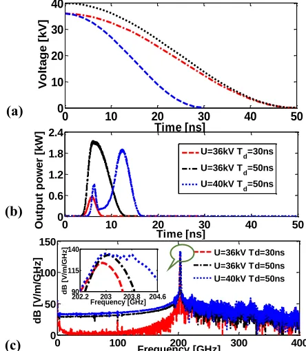
MAGIC-3D was used to verify the above CST Particle Studio simulations with a CW sheet electron beam and agrees well. To approximate the PS-SEB, a 1.7 A sheet electron beam with a pulsed voltage was used in the MAGIC-3D simulations. As shown in Fig. 6(a), the pulsed voltage has a sinusoidal decrease with a typical pulse duration Td of 50-100 ns. When a
sheet electron beam with a maximum voltage value Um of 36
kV and a Tdof 50 ns is injected into the interaction circuit, an
output pulse with peak power of 2.1 kW and pulse width Tp of
[image:4.612.51.299.461.676.2]11 ns is predicted, as shown in Fig. 6(b). The frequency
Fig. 6 MAGIC-3D simulation results. (a) Voltage pulse with different
Um (36 kV and 40 kV) and different Td (30 ns and 50 ns). (b) Pout
versus time. (c) Frequency spectrum of the Ez-field observed at the
output port.
30 32 34 36 38 40
0 1 2 3 4 Voltage [kV] P o u t [k W ]
30 32 34 36 38 400
20 40 60 T s [ n s ] Pout Ts (a) (b)
0 5 10 15 20
0 1 2 3
Energy spread [%]
P o u t [k W ]
0 5 10 15 200
2 4 6 T s [n s ] Pout Ts
0 1 2 3 4 5 6
0 2 4 6
Conductivity X 107 [S/m]
P o u t [k W ]
0 1 2 3 4 5 60
5 10 15 T s [ n s ] Pout Ts (c)
0 2 4 6
0 2 4 6 8 Current [A] P o u t [k W ]
0 2 4 6 0
9 18 27 36 T s [ n s ] Pout Ts (d) 30 32 34 36 38 40 190 195 200 205 Voltage [kV] F re q u e n c y [ G H z]
0 100 200 300 400
0 50 100 150 Frequency [GHz] d B [ V /m /G H z] U=36kV Td=30ns U=36kV Td=50ns U=40kV Td=50ns (a) (b)
0 10 20 30 40 50
0 0.6 1.2 1.8 2.4 Time [ns] O u tp u t p o w e r [k W ] U=36kV T d=30ns U=36kV T d=50ns U=40kV T d=50ns (c)
202.2 203 203.8 204.6 90 115 140 Frequency [GHz] d B [ V /m /G H z]
0 10 20 30 40 50
spectrum of the Ez-field observed at the output port is pure, as
shown in Fig. 6(c).
Um and Td are adjustable by changing the external circuit
parameters of the pseudospark discharge [14]. When Um is 40
kV there are two peaks in the Pout versus time curve, as shown
in Fig. 6(b). This is probably caused by two different resonant modes respectively operating in the two regions. When the electron beam voltage decreases from 40 to 37 kV, the non-2π mode will be formed in the cavity, which corresponds to the first region. Similarly, the 2π mode will be generated when the electron beam voltage reduces to 36 kV, corresponding to the second region. As the electrons have more intense beam-wave interaction with the 2π mode than the non-2π mode, the second region has a much higher peak value. As shown in Fig. 6(c), the frequency spectrum for Um of 40 kV is not very clean. This
interaction can be avoided by lowering the electron beam voltage. With a higher Td, the electron voltage will decrease
more slowly. Consequently, the electron voltage will stay in the oscillating voltage region over a longer time, resulting in an effective beam-wave interaction over a longer time. In a certain range, Pout and Tp will become larger when increasing Um or Td.
A thermal simulation was conducted to estimate the temperature distribution of the experimental structure. Simulation shows that the maximum temperature is about 169 °C assuming an applied voltage of 40 kV, a 34 A beam current injected into the beam tunnel, a 95% beam interception, a 100 ns pulse width, a 100 Hz pulse repetition frequency and the intercepted beam power is uniformly distributed on the beam tunnel. Such a temperature is lower than the copper’s heat-resistant temperature. For a higher temperature rise, such as caused by a higher pulse repetition or a longer pulse width, water or air cooling could be used to decrease the temperature.
IV. COMPARISONS OF THE PS-SEB AND PS-PEBEIOS
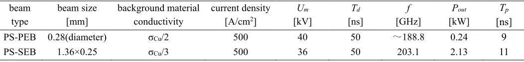
The most obvious difference in the interaction circuit of the PS-PEB [4] and PS-SEB G-band EIOs is the beam tunnel. The PS-SEB EIO has a rectangular beam tunnel with large cross section size, while the PS-PEB EIO has a circular cross section. Such a change will have an effect on the beam cross section, the dispersive characteristics, the coupling impedance, and the cavity properties of the resonant SWS, thus affecting the whole tube performance.
Comparisons in the tube performance are made between these two EIOs. As shown in table 1, the input parameters used in the beam-wave interaction MAGIC-3D simulations for both EIOs are the same or similar. Compared with the PS-PEB EIO, the PS-SEB EIO has achieved much better tube performance. The output power produced by the PS-SEB EIO is nearly eight times higher, even when considering a larger copper loss. The pulse width of the output signal is nearly 22% larger. The
planar interaction circuit is compatible with the 2-D planar manufacturing technique. The beam tunnel and gaps in the PS-SEB EIO can be wire cut from a single copper block in one process. The discharge voltage is smaller, which is beneficial for achieving a compact voltage supply.
The improved performance for the PS-SEB EIO is probably caused by the several following factors. Firstly, the beam cross section has been increased, which is probably the most important factor, the beam cross-sectional area in the PS-SEB and PS-PEB EIOs are about 0.34 mm2 and 0.06 mm2, respectively. Secondly, a wider voltage oscillating region is achieved, 8 kV in the PS-SEB EIO and 7 kV in the other case. Thirdly, the gap number has increased from 7 gaps to 11 gaps, which tends to result in a higher R/Q and thus a more intense interaction. Although the number of gaps has increased, the total circuit length in these two EIOs is similar. In addition, the beam focusing principle is basically similar in these two kinds of PS electron beams, thus leading to a similar beam current loss caused by the electron interception.
Compared with the PS-PEB W-band EIO in reference [5], the G-band EIO in this paper also has several improvements. (1) A larger beam tunnel cross section, which allows more electrons to be propagated through the circuit, 0.5 mm in diameter for the W-band EIO and 2×0.25 mm2 in area for the G-band EIO. (2) The interaction circuit was optimized to achieve a wider operating voltage range (31-39 kV), which is nearly doubled compared with that of the W-band EIO. (3) A higher operating frequency reduces the interaction length. The total length of the interaction circuit is about 5.55 mm, which is nearly halved compared with that of the W-band EIO. These improvements are beneficial to alleviate the disadvantageous effects fromlarge beam current loss and high energy spread, which are two of the main factors leading to the W-band EIO experimental results being less than the predictions.
V. CONCLUSION
[image:5.612.44.570.657.720.2]To make full use of the advantageous merits of the sheet electron beam and PS electron beam, a PS-SEB is proposed and utilized to drive a planar G-band EIO, aiming to achieve a compact sub-THz radiation source with high radiation power. PIC-3D simulations of this EIO exhibit very promising and attractive results with a peak radiation power of 2.1 kW at approximately 0.2 THz. A comparison shows that significant improvements have been obtained especially in the radiation power compared with a previously designed PS-PEB EIO. The planar interaction circuit is under fabrication, and the designed PS-SEB EIO will be built and experimentally tested in the future with an aim to achieve a better agreement between the simulation and experiment.
Table 1 Performance comparisons between the PS-SEB and PS-PEB EIOs at G-Band.
beam type
beam size [mm]
background material conductivity
current density [A/cm2]
Um
[kV]
Td
[ns]
f [GHz]
Pout
[kW]
Tp
[ns]
PS-PEB 0.28(diameter) σCu/2 500 40 50 ~188.8 0.24 9
PS-SEB 1.36×0.25 σCu/3 500 36 50 203.1 2.13 11
REFERENCES
[1] P. H. Siegel, “Terahertz technology,” IEEE Trans. Microwave
Theory Tech., vol. 50, no. 3, pp. 910–928, Mar. 2002.
[2] J. H. Booske et al., “Vacuum electronic high power terahertz
sources,” IEEE Trans. Terahertz Sci. Technol., vol. 1, no. 1, pp. 54–75, Sep. 2011.
[3] M.A. Basten, J.C. Tucek, D.A. Gallagher, and K.E. Kreischer, “233 GHz high power amplifier development at Northrop Grumman,” 17th Int. Conf. Vacuum Electronics (IVEC), Monterey, CA, USA, May 2016, pp. 43–44, Monterey, CA, April 2016.
[4] Y. Yin, W. He, L. Zhang, et al.,“Preliminary design and optimization of a G-band extended interaction oscillator based on a pseudospark-sourced electron beam,” Phys. Plasmas, vol. 22, no. 7, pp. 073102-1–073102-6, Jul. 2015.
[5] Y. Yin, W. He, L. Zhang, et al., "Simulation and experiments of a W-band extended interaction oscillator based on a pseudospark-sourced electron beam," IEEE Trans. Electron
Devices, vol. 63, no. 1, pp. 512-516, Jan. 2016.
[6] R. Dobbs, B. Steer, “Extended interaction sources above 220,”
36th Int. Conf. Infrared, Millimeter and Terahertz Waves
(IRMMW-THz), Houston, USA, 2011, pp. 1.
[7] J. Pasour, E. Wright, K. Nguyen, and B. Levush, “Compact, multi-kW sheet beam oscillator at 94 GHz,” 41th Int. Conf.
Plasma Sciences (ICOPS), Washington DC, USA, 2014, pp. 1.
[8] H. J. Liu; L. Meng; Y. Yin, et al, “Design of a high efficiency
W-band extended interaction oscillator,” International Workshop on Microwave and Millimeter Wave Circuits and System
Technology (MMWCST), Emeishan, China, Oct, 2013, pp.
355-356
[9] Z. Wu; K. C. Zhang; S. G. Liu, “Sheet-beam 0.225THz extended interaction oscillator,” 36th Int. Conf. Infrared, Millimeter, and
Terahertz Waves (IRMMW-THz) Houston, USA, 2011, pp.1-2.
[10]A. W. Cross, H. Yin, W. He, et al., “Generation and application
of pseudospark-sourced electron beams,” J. Phys. D: Appl. Phys., vol. 40, no. 7, pp. 1953-1956, Mar. 2007.
[11]H. Yin, A.W. Cross, A. D. R. Phelps, et al., “Propagation and
post-acceleration of a pseudospark-sourced electron beam,” Appl.
Phys. Lett., vol. 91, no.8, pp. 5419-5422, Apr. 2002.
[12]D. Bowes et al., “Visualization of a pseudospark-sourced electron beam,” IEEE Trans. Plasma Sci., vol. 42, no. 10, pp. 2826–2827, Oct. 2014.
[13]H. Yin, A. W. Cross, W. He, et al., “Millimeter wave generation from a pseudospark-sourced electron beam,” Phys. Plasmas, vol. 16, no. 6, pp. 063105-1–063105-6, Jun. 2009.
[14]W. He, L. Zhang, D. Bowes, H. Yin, et al., "Generation of broadband terahertz radiation using a backward wave oscillator and pseudospark-sourced electron beam," Appl. Phys. Lett., 107, no. 13, pp. 133501-1–133501-4, Sep. 2015.
[15]H. Yin, G. R. M. Robb, W. He, et al., “Pseudospark-based electron beam and cherenkov maser experiments,” Phys.
Plasmas., vol. 7, no.12, pp. 5195-5205, Dec. 2000.
[16]J. Pasour, E. Wright, K. T. Nguyen, et al., “Demonstration of a
multikilowatt, solenoidally focused sheet beam amplifier at 94 GHz,” IEEE Trans. Electron Devices, vol. 61, no. 6, pp. 1630– 1636, Jun. 2014.
[17]Y. Shin, J. Wang, L. R. Barnett, et al., “Particle-in-cell simulation analysis of a multicavity W-Band sheet beam klystron,” IEEE
Trans. Electron Devices, vol. 58, no. 1, pp. 251–258, Jan. 2011.
[18] A. Baig, Y. M. Shin, and L. R. Barnett, “Design, fabrication and RF testing of near-THz sheet beam TWTA,” IEEE Trans.
Terahertz Sci. Technol., vol. 4, no. 4, pp. 181–207, Apr. 2011.
[19] G. Liu, J. X. Wang, G. X. Shu, et al, “RF Design, thermal
analysis, and cold test of a Ku-Band continuous wave sheet beam traveling wave tube,” IEEE Trans. Electron Devices, vol. 62, no. 11, pp. 3844–3850, Nov. 2015.
[20]G. X. Shu, J. X. Wang, G. Liu, et al, “An improved slow-wave
structure for the sheet-beam traveling-wave tube,” IEEE Trans.
Electron Devices, vol. 63, no. 5, pp. 2089–2096, May. 2016.
[21]C. Paoloni, D. Gamzina, L. Himes, et al., “THz backward-wave
oscillators for plasma diagnostic in nuclear fusion,” IEEE Trans.
Plasma Sci., vol. 44, no. 4, pp. 369–376, Apr. 2016.