International Journal of Innovative Technology and Exploring Engineering (IJITEE) ISSN: 2278-3075, Volume-8 Issue-9, July 2019
Retrieval Number:H6770068819/19©BEIESP
Abstract: A multilevel inverter with half bridge cells and seven switches is implemented for Solar PV based applications. The photovoltaic panels are employed to replace the DC sources and maximum power is ensured by employing a boost converter andPerturb and Observe(P&O) algorithm. The generation of switching pulses is carried by usingNearest Level Control(NLC) technique.The operating principle of the proposed multilevel inverter(MLI) is verified by utilizing different loads and the experimental results are obtained through prototype testing.
Index Terms:Asymmetrical,Cascaded H-bridge, Half bridge, Perturb and Observe,Nearest Level Control(NLC)
I. INTRODUCTION
The main components of renewable energy are Solar, wind and hydro. Compared to other renewable sources available, the solar energy and wind energy have gained more prominence[1]. The solar energy has various advantages like reduction of cost, does not cause pollution and it is available constantly throughout the daytime. MLI combined with solar PV systems is utilized in standalone as well as grid connected systems[2,3].
MLIs are classified as (1)Flying Capacitors (FCs),(2)Neutral Point Clamped (NPC) and (3)Cascaded H-Bridge (CHB). Among all these topologies, CHB possesses various advantages like high modularity and ability to reach medium output voltage levels with the help of low-voltage components [5-8]. These structures are composed of a series connection of several single-phase H- Bridge inverters. The cascaded multilevel inverter can be divided into symmetric and asymmetric forms based on the magnitudes of the DC sources[9-11]. In symmetric form, the DC sources have equal values and these offer modularity and the option to extend the capacity. And the asymmetric structure has unequal values but has the option of increasing the voltage levels with the same component count[12]. The major issue in multilevel inverters is the proportionate increase in the count of the semiconductor devices employed with increase in the number of levels, whereby leading to increased cost of the system. In recent years, researchers have also developed a large number of topologies with reduced component count[13-15]. The MLIs utilizing lesser number of devices and operating at lower switching frequency helps in improving the efficiency of PV inverter which are used for standalone applications.
The maximum power can be obtained from PV by using a suitable MPPT algorithm. The two primary parameters which influence the voltage generated from the solar areIrradiation and temperature[16, 17].
Revised Manuscript Received on July 05, 2019
Abeera Dutt Roy, Research Scholar, School of Electrical Engineering, VIT University, Chennai.
ChandrahasanUmayal, Associate Professor, School of Electrical Engineering, VIT University, Chennai.
In the literature, various MPPT techniques are available and among them the P&O algorithm is used in this paper. Anovel seven level cascaded MLI topology using reduced devices is presented. The proposed MLI is synthesized by combining H-bridge inverter and half bridge
module. A
boost converter along with P&O algorithm ensures maximum power from the PV which is used as a source of the proposed MLI. A prototype is developed which provides the experimental results to confirm the working principle of this architecture.It has the following advantages: (i)considerable reduction in component count (ii)marginal reduction in the requirement of DC sources (iii)reduced switching and conduction losses(iv)compact in size (v)Capability to produce negative voltage levels without a separate H-bridge inverter at the output.II. MODELLINGOFPV
In the proposed work, the PV arrayis usedwhose parameters are provided in the table- I. The PV cell shown in Fig is represented by a current source which is placed in parallel with diode and two resistances are added (a series and shunt resistance).The mathematical model for this array is as follows[19]: sh pv se pv V I R V ph pv
R
I
R
V
e
I
I
I
T pv se pv
)
1
(
( 0(1)
Where
pvI
= PV
cell output currentpv
V
= PV cell outputvoltage0
I
= saturation currentT
V =
nKT
/
q
= thermal voltage(n
= emission coefficientfactor of PV cell)
se
R
=series resistancesh
R
= shunt resistanceK
= Boltzmann constantT
= cell temperature
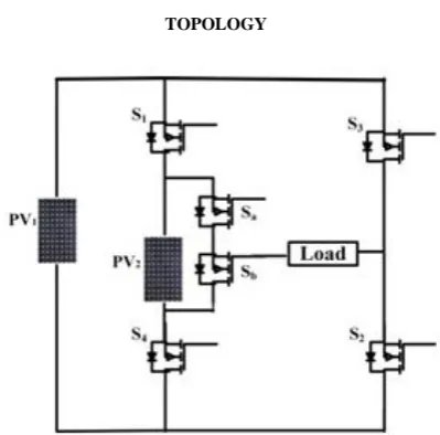
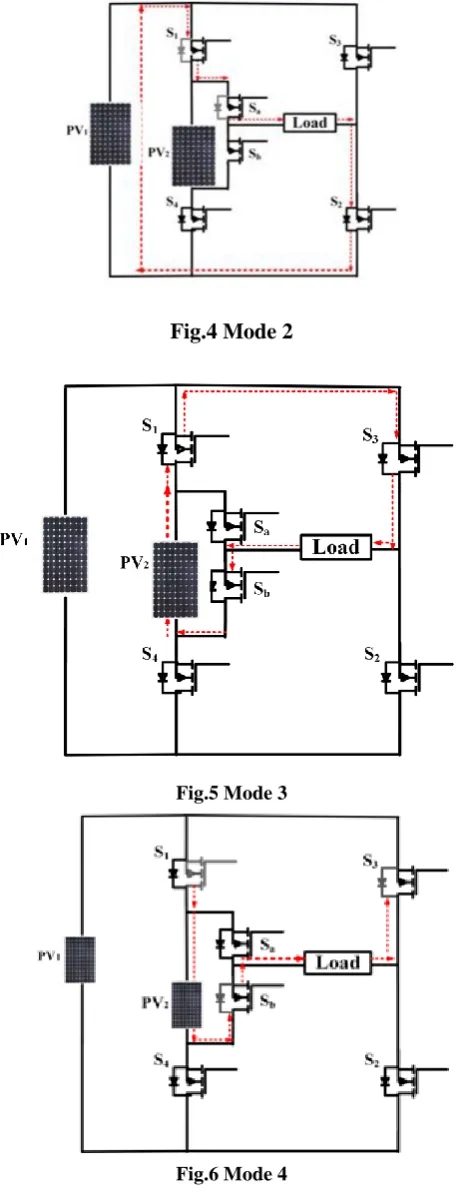
Implementation of a Solar based Seven Level
Asymmetrical Multilevel Inverter Topology
with reduced device count
device count
Fig. 1: Equivalent circuit of PV cell III.PROPOSED PV BASED MULTILEVEL INVERTER
TOPOLOGY
Fig. 2:Circuit of proposed topology for 7-level inverter The power circuit of proposed MLI is shown in Fig. (1). The proposed MLI consists of two voltage sources with the ratios of 1:2((V1=100V, V2= 200V).The H-bridge
module of the topology consists of four MOSFET with antiparallel diodes(S1,S2,S3 and S4) . The half bridge module
of the MLI consists of two MOSFET switches with antiparallel diodes(Sa,Sb) as shown in Fig. 1.A resistive load
and combination of resistive and inductive loads are used to validate the performance of the MLI. The circuit shown in Fig. 1can be generalized for higher voltage levels by introducing suitable number of voltage sources and half bridge modules in betweenS1 and S4. It is observed from
Fig.1 that switch
combinations of S1, S4 and S3, S2 should not be turn on
[image:2.595.79.249.59.164.2]simultaneously to avoid the sources from being short circuited. The different switching states of the seven level inverter where 1 and 0 signify ON and OFF states of the devices are shown in Table I. The Figs. 2 to 9 portray the operating modes to extract various levels of the output voltage. It highlights the usage of only three devices to generate the output voltages whereas the conventional cascaded structure uses 6 devices. This leads to the reduction of power dissipation and the
switching losses.
The various power components required for this topology is illustrated in Table II.Table I. Switching States of Proposed Topology Voltage Level S1 S2 S3 S4 Sa Sb
V1 0 0 1 1 0 1
V2 0 1 0 1 1 0
(V1+ V2) 0 0 1 1 1 0
0 0 1 0 1 0 1
0 1 0 1 0 1 0
-V1 1 1 0 0 1 0
-V2 1 0 1 0 0 1
-(V1+ V2) 1 1 0 0 0 1
Table II. Required power components for the proposed topology
Parameters Values
Count of Output levels
Total count of switches
Maximum value of output voltage Vdc
PIV (4/7) Vdc
[image:2.595.70.270.215.412.2]Number of On state switches +3
Fig.3 Mode 0
[image:2.595.303.554.270.830.2]International Journal of Innovative Technology and Exploring Engineering (IJITEE) ISSN: 2278-3075, Volume-8 Issue-9, July 2019
[image:3.595.320.533.54.253.2]Retrieval Number:H6770068819/19©BEIESP
Fig.4 Mode 2
Fig.5 Mode 3
Fig.6 Mode 4
Fig.7 Mode 5
IV. MPPTCONTROL
[image:3.595.52.284.58.656.2]Nowadays, MPPTis very common to extract maximum power from PV panels[17]. Irradiation and temperature are the two major factors which affect the generated voltage from PV system. ]. It also helps to maintain optimum performance of the system when there are deviations in the climatic conditions or Standard Test Condition values[18]. The P&O algorithm is used for the proposed topology which is shown in the Fig. 8.
Fig. 8: Algorithm of P&O
This algorithm is instrumental in changing(i.e. increasing or decreasing) the current or voltage at regular intervals and the present power is compared with the previousiterative power to maximize the output power. If an increase in the output power is observed, then the voltage perturbation occurs in the same direction otherwise the perturbation should be carried out against the initial direction. The advantage of this method is when the speed of execution of the P&O increases, then the losses incurred by the system reduces.
V. DESIGN OF BOOST CONVERTER
[image:3.595.320.540.405.539.2]device count
Hence in such variable and intermittent power source [image:4.595.307.547.545.658.2]needs impedance matching between the source and load for maximum power transfer[19,20]. The boost converter is introduced to match impedance for maximum power transfer and the circuit diagram of the same is provided in Fig 9.
Fig. 9: Boost converter
The State and Output equations at DT mode is obtained by applying KVL on loop abcd
=
(1)
BY applying KVL on loop efgh
=
(2)
But the capacitor voltage delivers the load current,
henceic= -iload = (3)
Now equn (2) can be rewritten as
=
=
(4)
Now state equns can be rewritten in matrix form as,
=
+ (5)
A1B1
Now the output equation is given by,
(6)
State and Output equations at (1-D)T mode
By applying KVL on loop abehdc
= (7)
= L
+ (8)
=
- (9)
By applying KCL on node e
+ (10)
=
+ (11)
= - (12)
Now state equations can be rewritten in matrix form as,
(13)
And the output equation is given as it is
(14)
In this paper, circuit averaging is applied to compute state and output matrices. Hence,
(15)
(16)
(17)
Now, substituting the value of A 1, B 1, C 1, A 2, B 2, C 2 from
equations 5,6, 13, 14
=
(18)
(19)
In the above equations, the variables with superscript of dash represent the transient part and without dashrepresent the steady state part. Now the first right hand term of equation (18) can be splitted and rewritten as
International Journal of Innovative Technology and Exploring Engineering (IJITEE) ISSN: 2278-3075, Volume-8 Issue-9, July 2019
Retrieval Number:H6770068819/19©BEIESP
+ (20)
By equating the steady state part to zero, the above expression can be reduced to the following including duty cycle in the input vector
(21)
Now, the state equation for the small signal model of the boost converter can be written as
A=
(22)
B= (23)
C=
(24)
VI.MODULATIONSCHEME
The Nearest Level Control (NLC) methodology is utilised for producing the switching pulses at the fundamental switching frequency. It generates reduced switching losses and quite simple to implement for prototyping[21,22,23]. It produces higher harmonics for lower levels of the output waveform.
The harmonic voltage in respect to the Fourier series is shown below: ) sin( ) ( cos nπ dc 4V 1,3,5 n (t) 0
V n t
k
n
(25)
1 2 1 V Vrms 1 V 3.57
p Vh
THD
(26) 2 1 cos 2 2
p p x V V k N k odd p rms L
(27)where p = 3, 5, 7…. and Vh provides the order in which the
harmonics increases and Vrms is the rms value of the output
voltage.
V1 is the voltage at the fundamental frequency which is
given by equation (6).
(28)
= , k=1,2,3,……Nl (29)
The values of 1, 2……NL are the switching angles which
[image:5.595.320.528.231.365.2]are calculated by using equation (29)
[image:5.595.50.261.513.647.2]Fig. 10 Simulation results for R Load
Fig. 11Simulation resultsfor RL Load VII.SIMULATIONRESULTS
The proposed topology is simulated on a R2015b MATLAB platform and voltages chosen are (V1=100V, V2=
200V). This produces seven levels at the output across a resistive inductive load of 80 and 100mH respectively. It uses NLM technique for producing switching pulses as it generates reduced switching losses. The simulation results ofoutput voltage and current are for R load are shown in Fig. 10. And both the parameters are in phase with each other. The FFT spectrum of the output voltage is shown in Fig.12 and %THD of output voltage is 10.1%.Thesimulation results of output voltage and current waveforms for RL load is shown in Fig.11 depicts theIt is seen here that the resistive inductive load acts like a low pass filter which generates a ripple free waveform of the output current.The %THD of output voltage and current which are illustrated in the Figs.13 and 14are 10.05% and 0.63%.
[image:5.595.317.529.610.714.2]device count
Fig. 13 Output voltage and current for RL load
Fig. 14.FFT spectrum for output voltage for RL load
VIII.EXPERIMENTALRESULTS
[image:6.595.319.536.67.249.2]A prototype is fabricated in the laboratory. The NLM technique was utilised for generating the switching pulses by using the controller ATMEGA32P. The experiments results of output voltage and current for R load is shown in Fig.15.The RMS value of output voltage and current are 110.33V and 4.5A. The voltage THD of 11.3% is shown in Fig.16 .The hardware results for RL load is shown in Fig.17. The output current lags the output voltage because of the inductive nature of the load which acts like low pass filter. The RMS value of output voltage and current are 113.1V and 4.4A respectively. The values of voltage and current THD for RL load shown in Fig.18 and Fig.19 are 11.1% and 1.6% respectively. Thus, the experimental results are developed for resistive and inductive loads which are displayed in Table IV.
Fig. 15 Hardware results for R Load
[image:6.595.62.272.236.390.2]Fig. 16 Output Voltage spectrum for R Load
[image:6.595.321.546.283.485.2]Fig. 17Hardware results for RL Load
[image:6.595.322.534.526.717.2] [image:6.595.59.287.666.789.2]International Journal of Innovative Technology and Exploring Engineering (IJITEE) ISSN: 2278-3075, Volume-8 Issue-9, July 2019
[image:7.595.72.270.55.184.2]Retrieval Number:H6770068819/19©BEIESP
Fig. 19Output Current spectrum for RL Load
TableIII. Specifications of the Hardware Prototype
Parameters Values
Output Voltage 110V
Output Current 4.5A
Switches IRF640
Optoisolator TLP250
Controller ATMEGA32P
Resistance 50
Inductance 32mH
Table IV. Experimental results for R and RL loads
Param eters Output Voltage( V) Output Current( I) TH DV %
THDI %
R load 110.33 4.5 11.3 11.3
RL Load
113.06 4.4 11.1
1.6
CONCLUSION
An asymmetrical MLI is implemented and P&O technique is utilized to maximize the power achieved through boost converter. The novelty of this structure lies in reducing the switch count and the requirement of DC sources. This also leads to the reduction of switching and conduction losses. The advantage of this topology is the ability to produce negative voltage levels without the addition of external H-bridge.The experimental results obtained confirms the feasibility of this topology.
REFERENCES
1. Alepuz, S., Busquets-Monge, S., Bordonau, J., et al.: ‘Interfacing renewable energy sources to the utility grid using a three-level inverter’, IEEE Trans.Ind.Electron., 2006, 53, (5), pp. 1504–1511 2. Patrao, I., Garcerá, G., Figueres, E., et al.: ‘Grid-tie inverter topology
withmaximum power extraction from two photovoltaic arrays’, IET Renew. PowerGener., 2014, 8, (6), pp. 638–648
3. 3 Rodriguez, J., Bernet, S., Lizama, I., et al.: ‘A survey on neutral pointclampedinverters’, IEEE Trans. Ind. Electron., 2010, 57, (7), pp. 2219–2230
4. M. K. Das, K. C. Jana, and A. Sinha, “Performance evaluation of an asymmetrical reduced switched multi-level inverter for a grid-connected PV system,” IET Renew. Power Gener., vol. 12, no. 2, pp. 252–263, 2017.
5. M. Malinowski, K. Gopakumar, J. Rodriguez, and M. A. Pérez, “A Survey on Cascaded Multilevel Inverters,” IEEE Trans. Ind. Electron., vol. 57, no. 7, pp. 2197–2206, Jul. 2010.
6. I. Colak, E. Kabalci, and R. Bayindir, “Review of multilevel voltage source inverter topologies and control schemes,” Energy Convers. Manag., vol. 52, no. 2, pp. 1114–1128, Feb. 2011.
7. Fang Zheng Peng, “A generalized multilevel inverter topology with self-voltage balancing,” IEEE Trans. Ind. Appl., vol. 37, no. 2, pp. 611–618, 2001.
8. A. Nabae, I. Takahashi, and H. Akagi, “A New Neutral-Point-Clamped PWM Inverter,” IEEE Trans. Ind. Appl., vol. IA-17, no. 5, pp. 518–523, Sep. 1981.
9. M. M. Hasan, A. Abu-Siada, and M. S. A. Dahidah, “A three-phase symmetrical DC-Link multilevel inverter with reduced number of DC Sources,” IEEE Trans. Power Electron., vol. 33, no. 10, pp. 8331–8340, 2018.
10. M. R. J. Oskuee, M. Karimi, S. N. Ravadanegh, and G. B. Gharehpetian, “An Innovative Scheme of Symmetric Multilevel Voltage Source Inverter with Lower Number of Circuit Devices,” IEEE Trans. Ind. Electron., vol. 62, no. 11, pp. 6965–6973, 2015. 11. C. Dhanamjayulu and S. Meikandasivam, “Implementation and
Comparison of Symmetric and Asymmetric Multilevel Inverters for Dynamic Loads,” IEEE Access, vol. 6, pp. 738–746, 2018.
12. E. Samadaei, M. Kaviani, and K. Bertilsson, “A 13-levels Module (K-Type) with two DC sources for Multilevel Inverters,” IEEE Trans. Ind. Electron., vol. PP, no. c, pp. 1–1, 2018.
13. K. K. Gupta, A. Ranjan, P. Bhatnagar, L. K. Sahu, and S. Jain, “Multilevel Inverter Topologies With Reduced Device Count: A Review,” IEEE Trans. Power Electron., vol. 31, no. 1, pp. 135–151, Jan. 2016.
14. E. Babaei, S. Laali, and Z. Bayat, “A Single-Phase Cascaded Multilevel Inverter Based on a New Basic Unit With Reduced Number of Power Switches,” IEEE Trans. Ind. Electron., vol. 62, no. 2, pp. 922–929, Feb. 2015.
15. A. Z. Gharehkoushan, E. Babaei, R. S. Alishah, M. Sabahi, and S. H. Hosseini, “Optimal design of new cascade multilevel converter topology based on series connection of extended sub-multilevel units,” IET Power Electron., vol. 9, no. 7, pp. 1341–1349, Jun. 2016. 16. V. J. Chin, Z. Salam, and K. Ishaque, “Cell modelling and model
parameters estimation techniques for photovoltaic simulator application: A review,” Appl. Energy, vol. 154, pp. 500–519, Sep. 2015.
17. J. Ahmed and Z. Salam, “An improved perturb and observe (P&;O) maximum power point tracking (MPPT) algorithm for higher efficiency,” Appl. Energy, vol. 150, pp. 97–108, Jul. 2015.
18. S. B. Kjaer, J. K. Pedersen, S. Member, and F. Blaabjerg, “A Review of Single-Phase Grid-Connected Inverters for Photovoltaic Modules,” vol. 41, no. 5, pp. 1292–1306, 2005.
19. A. Ravi, P. S. Manoharan, and J. V. Anand, “Modeling and simulation of three phase multilevel inverter for grid connected photovoltaic systems,” vol. 85, pp. 2811–2818, 2011.
20. M. Farhat, O. Barambones, and L. Sbita, “A new maximum power point method based on a sliding mode approach for solar energy harvesting,” Appl. Energy, vol. 185, pp. 1185–1198, 2017.
21. Kumar, R., Deepa,T. An Improved Low Switching Frequency Modulation Scheme for a Symmetric CCS-Multilevel Inverter. International Journal of Power Electronics. In Press.
22. Kumar, R., Deepa,T. Line Frequency Sine Modulation - A Novel Modulation Scheme for Multilevel Inverters and Its Application Towards Enhanced Illumination of Incandescent Bulb. International Journal of Power Electronics, Vol. 10,N4,2019,DOI:10.1504/IJPELEC.2019.100173
device count
AUTHORS PROFILE
Abeera Dutt Roy is working as Research Scholar in School of Electrical Engineering, VIT university, Chennai campus. Her research interests are Multilevel inverters, modulation techniques.
Dr. C. Umayalobtained her PhD from Anna University in the year 2014. Currently working as Associate Professor in the School of Electrical Engineering, VIT University, Chennai campus.She has Authored around 16 International and 1National level research papers on Power Factor Correction in PMBLDC Drives. Author-1