Int. J. Electrochem. Sci., 8 (2013) 5183 - 5190
International Journal of
ELECTROCHEMICAL
SCIENCE
www.electrochemsci.orgDye-Sensitized Solar Cells with Sol-Gel Solution Processed
Ga-Doped ZnO Passivation Layer
Kyung Ho Kim*, Kazuomi Utashiro, Zhuguang Jin, Yoshio Abe, and Midori Kawamura
Department of Materials Science and Engineering, Kitami Institute of Technology, 165 Koen-cho, Kitami, Hokkaido 090-8507, Japan
*
E-mail: [email protected]
Received: 12 February 2013 / Accepted: 10 March 2013 / Published: 1 April 2013
The effects of a Ga-doped ZnO passivation layer between a TiO2 photoelectrode and an indium tin oxide (ITO) electrode on the performance of dye-sensitized solar cells (DSSCs) were investigated. It was found that the orientation, surface morphology, and resistivity of the ZnO thin films prepared by sol-gel solution strongly depended on the film thickness and the Ga doping amounts. The transmission of the ZnO films was very high (over 92 %) in the visible region for all the films. These properties are strongly related to the photovoltaic characteristics of DSSCs. With an optimized ZnO passivation layer, the cells showed significantly improved characteristics because of the suppression of interfacial recombination, which in turn led to improved efficiency. The cell with a 12-nm-thick Ga-doped ZnO (1.5 at.%) thin film showed a short-circuit current density (JSC) of 18.97 mA/cm2, an open-circuit voltage (VOC) of 0.69 V, a fill factor (FF) of 0.60, and a power conversion efficiency (PCE, ) of 7.85% under AM 1.5G illumination of 100 mW/cm2.
Keywords: Dye-sensitized solar cells, ZnO, Thickness, Ga dopant, Efficiency
1. INTRODUCTION
In recent years, dye-sensitized solar cells (DSSCs) have attracted significant attention because they are inexpensive and require simple fabrication processes; further, they can be fabricated on flexible substrates [1-3]. However, the efficiency of DSSCs is still lower than that of conventional silicon-based solar cells [4,5]. Several studies have shown that the deposition of HfO2 or TiO2 thin films on a porous TiO2 photoelectrode effectively prevents the recombination of electrons between the TiO2 photoelectrode and the electrolyte, resulting in improved cell efficiency [6-8].
annealing, the Ti nano layer was oxidized to form anatase-phase TiO2, which allowed for better light transmission than did the as-deposited metal-phase Ti nano-layer in the visible wavelength region. Cells based on a 5-nm-thick Ti layer showed improved short-circuit current density (JSC) and fill factor (FF) without any notable change in the open-circuit voltage (VOC), which resulted in better efficiency.
In this study, we discuss the photovoltaic characteristics of the DSSCs employing a ZnO passivation layer of various thicknesses and Ga doping amounts. It is well known that the electron mobility of ZnO is much higher than that of TiO2 and that the electrical properties of ZnO with a Ga dopant are effectively improved [10,11]. The enhanced electrical properties of the passivation layer might cause effective transfer of the generated electrons in the dye material from the TiO2 photoelectrode to the bottom transparent conducting electrode. There are several methods of preparing ZnO thin films, such as sputtering, pulsed laser deposition (PLD), electrochemical deposition, and the sol-gel process [12-15]. Among those, the sol-gel process affords high-purity products because of the high purity of the raw materials used and better homogeneity. It also allows easy control of the raw material composition [16,17].
2. EXPERIMENTAL
The passivation layer ZnO thin films were prepared using zinc acetate dihydrate [Zn(CH3COOH)22H2O, 0.1 M] as the precursor dissolved in ethanol, 2-methoxyethanol (ME), and Milli-Q solvents. Gallium nitrate hydrate [Ga(NO3)3nH2O] was used as the dopant, and the Ga-doped ZnO films were prepared with various Ga dopant amounts ranging from 0 to 2.0 at.%. After stirring at 60 °C for 3 h, the sol was aged at room temperature for 24 h. The sol was spin-coated on both quartz and ITO/glass substrates and then dried at 300 °C for 5 min. The films were then annealed at 430 °C for 30 min at a heating rate of 10 °C/min.
The thickness of the films was measured by variable-angle ellipsometry (MIZOJIRI, DVA-FL). The structure of the ZnO films was examined by X-ray diffraction (XRD, Bruker, D8ADVANCE) using a 2 scan. The surface morphologies were investigated by atomic force microscopy (AFM, SHIMADZU, SPM-9500J3) and field emission scanning electron microscopy (FESEM, JSM-6701F). The optical properties were investigated by ultraviolet-visible (UV-vis) spectroscopy (HITACHI, U-2910).
type cell with a 50-m-thick spacer, and an electrolyte containing lithium iodide (LiI, 0.5 M), iodine (I2, 0.05 M), and 4-tert-butylpyridine (TBP, 0.05 M) in acetonitrile/polyethylene glycol (4:1 v/v) was injected between the electrodes. The photovoltaic properties of the solar cells were measured using a Keithley 2400 Source Meter under AM 1.5G (100 mW/cm2), which was provided by a solar simulator (OTENTO-SUNIII). The cell area was 0.15 cm2.
3. RESULTS AND DISCUSSION
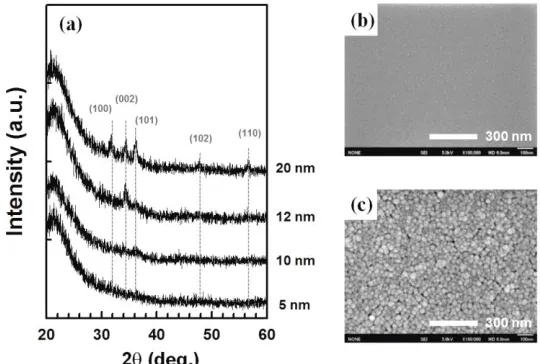
Figure 1(a) shows the XRD patterns of the ZnO thin films on the quartz substrates. The 5-nm-thick ZnO film is regarded as an amorphous phase, as shown in Fig. 1(b). With a further increase in the film thickness, intensities of crystalline peaks corresponding to the hexagonal wurtzite phase of ZnO (JCPDS Card No.36-1451) gradually increase, and then, the 20-nm-thick ZnO film is randomly oriented. The size of the nanocrystals was approximately 20 nm, as shown in Fig. 1(c). In the visible region, the transmission of the ZnO films (~ 92%) was almost the same as that of the quartz substrate, regardless of the film thickness. The interface layer located between the transparent conducting electrode and the TiO2 photoelectrode in the DSSCs needs to be highly transparent in the wavelength region of 400-700 nm, which is the main absorption region of the Ru dye material [19].
Figure 1. (a) XRD patterns of ZnO films with various thicknesses and (b,c) SEM images of ZnO films on quartz substrates: (b) 5-nm-thick, (c) 20-nm-thick.
[image:3.596.162.432.400.582.2]
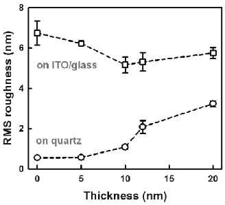
indicates that the ZnO thin films smoothed the rough morphology of the bare ITO/glass substrate [Fig. 3(d), RMS ~ 6.7 nm]. As shown in Figs. 3(b) and (e), the surface morphologies of the 5-nm-thick ZnO thin film could be clearly distinguished between the two different substrates. These results indicate that the ultrathin ZnO film on ITO is not continuous because of the presence of ITO nanocrystals. With a further increase in the film thickness, the difference in surface morphology between the substrates disappears, as shown in Figs. 3(c) and (f). It has been reported that a flat TiO2 passivation layer prevents electron recombination through the surface more effectively than does a rough surface [6].
Figure 2. RMS roughness of ZnO thin films on quartz (circle) and ITO/glass substrates (square)
Figure 3. 2D AFM images of (a-c) ZnO thin films on quartz and (d-f) on ITO/glass substrates: (a,d) bare substrates, (b,e) 5-nm-thick, (c,f) 20-nm-thick ZnO films.
Figure 4(a) shows the photo-current density-voltage (J-V) curves of DSSCs with the ZnO films of various thicknesses under AM 1.5G illumination. The DSSC with a 12-nm-thick ZnO layer shows excellent performance, with a short-circuit current density (JSC) of 16.99 mA/cm2, an open-circuit voltage (VOC) of 0.69 V, a fill factor (FF) of 0.54, and a consequent power conversion efficiency (PCE,
[image:4.596.212.376.210.359.2] [image:4.596.136.459.427.607.2]
4.17%. This indicated that the inclusion of a passivation layer results in a 55% improvement in the cell efficiency. Detailed cell parameters are summarized in Table 1. With an increase in the thickness of the ZnO film to 12 nm, the improved JSC could be therefore considered to be the result of the following: (1) the suppressed recombination of electrons between the TiO2 photoelectrode and the electrolyte and (2) the increase in the amount of the dye absorbed on the ZnO film [20]. As shown in Fig. 4(b), the onset of the dark current shifted to the higher forward bias in the presence of the ZnO passivation layer. This means that the recombination reaction between the electrons of the TiO2 photoelectrode and the triiodide ions in the electrolyte is effectively suppressed [6,21]. The suppressed recombination also gives rise to an increase in the FF from 0.49 to 0.54 [10,22]. However, with a further increase in the ZnO film thickness to 20 nm, the values of JSC and FF decrease slightly, which led to fewer electrons being transferred to the bottom electrode [23]. This decrease in JSC and FF might be because the electrical properties of the randomly oriented 20-nm-thick ZnO film are poorer than those of the preferential c-axis-oriented 12-nm-thick ZnO film [24].
[image:5.596.121.474.323.456.2]Figure 4. J-V curves of DSSCs with TiO2/ZnO samples under (a) illumination and (b) dark conditions.
Table 1. Detailed cell parameters of DSSCs with ZnO passivation layers of various thicknesses under AM 1.5G illumination.
Thickness (nm)
JSC
(mA/cm2)
VOC
(V)
FF
(-)
(%)
0 12.77 0.67 0.49 4.17
5 13.39 0.68 0.51 4.61
10 15.40 0.67 0.53 5.40
12 16.99 0.69 0.54 6.45
20 16.25 0.67 0.53 5.80
[image:5.596.51.545.549.654.2][image:6.596.110.485.220.354.2]
electrical resistivity of the Ga-doped ZnO films. Until reaching 1.0 at.% Ga doping on ZnO, the resistivity could not be measured. As seen from the figure, upon reaching 1.0 at.% Ga doping, resistivity decreases, reaching a minimum at 1.5 at.% Ga doping. It then increases with further increasing of the Ga doping amount. It is well known that the Ga dopant is incorporated into the ZnO in the Zn sites, supplying one free electron to the conduction band until the maximum solubility of Ga into the ZnO is reached. However, at higher doping levels, the Ga does not replace more Zn sites; it works as an impurity instead, causing deterioration in the electrical resistivity [11].
Figure 5. (a) UV-vis transmittance spectra and (b) electrical resistivity of 12-nm-thick ZnO films as a function of Ga doping amounts.
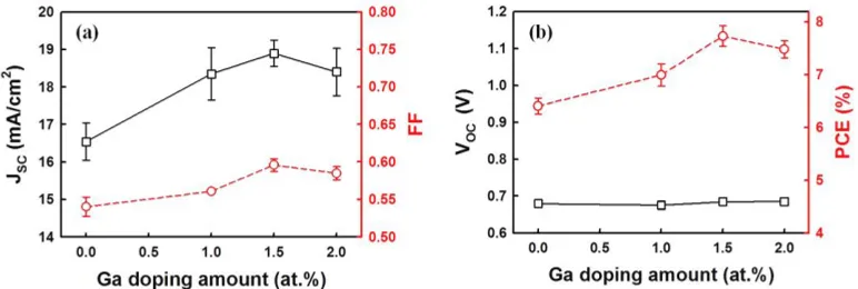
Figure 6. Photovoltaic parameters of the DSSCs employing Ga-doped ZnO films: (a) Jsc vs. FF and (b) Voc vs. PCE.
[image:6.596.106.492.429.559.2]
4. CONCLUSIONS
The structural, optical, and electrical properties of the ZnO thin films prepared using a sol-gel solution are significantly related to the film thickness and the Ga doping amount. When a 12-nm-thick Ga-doped ZnO passivation layer was inserted between the TiO2 photoelectrode and the ITO/glass substrate, the cell exhibited an improved efficiency of 7.85% as compared to the cells with only TiO2 sample (, 4.17%). The addition of the Ga-doped ZnO passivation layer prepared by the sol-gel process is a low-cost, simple, and effective method for improving cell performance.
ACKNOWLEDGEMENT
This work was supported by the Grant-in-Aid for Young Scientists (B) (24760245) from the Japan Society for the Promotion of Science (JSPS).
References
1. B. O’Regan and M. Grätzel, Nature, 353 (1991) 737-740. 2. M. Grätzel, Inorg. Chem., 44 (2005) 6841-6851.
3. L-Y. Lin, C-P. Lee, P. Vittal and K-C. Ho, J. Power Sources, 195 (2010) 4344-4349.
4. M-A. Tsai, P-C. Tseng, H-C. Chen, H-C. Kuo and P. Yu, Optics Express, 19 (2011) A28-A34. 5. K. Yamamoto, A. Nakajima, M. Yoshimi, T. Sawada, S. Fukuda, T. Suezaki, M. Ichikawa, Y. Koi,
M. Goto, T. Meguro, T.Matsuda, M. Kondo, T. Sasaki and Y. Tawada, Solar Energy, 77 (2004) 939-949.
6. K-I. Jang, E. Hong and J.H. Kim, Korea J. Chem. Eng., 29 (2012) 356-361.
7. H-F. Wang, L-Y. Chen, W-N. Su, J-C. Chung and B-J. Hwang, J. Phys. Chem. C 114 (2010) 3185-3189.
8. B. Bills, M. Shanmugam and M.F. Baroughi, Thin Solid Films, 519 (2011) 7803-7808. 9. K.H. Kim, T. Inoue, Y. Abe and M. Kawamura, in preparation.
10. K. Park, Q. Zhang, B.B. Garcia, X. Zhou, Y-H. Jeong and G. Cao, Adv. Mater., 22 (2010) 2329-2332.
11. K.T. Ramakrishna Reddy, T.B.S. Reddy, I. Forbes and R.W. Miles, Surf. Coat. Tech., 151-152 (2002) 110-113.
12. S.J. Lim, S. Kwon and H. Kim, Thin Solid Films, 516 (2008) 1523-1528.
13. T. Ohshima, R.K. Thareja, T. Ikegami and K. Ebihara, Surf. Coat. Tech., 169-170 (2003) 517-520. 14. A.B. Moghaddam, T. Nazari, J. Badraghi and M. Kazemzad, Int. J. Electrochem. Sci., 4 (2009)
247-257.
15. M. Ohyama, H. Kouzuka and T. Yoko, Thin Solid Films, 306 (1997) 78-85. 16. D. Ganguli, Bull. Mat. Sci., 15 (1992) 421-430.
17. R.F.S. Lenza and W.L. Vasconcelos, Mat. Res., 5 (2002) 497-502.
18. K.H. Kim, T. Okubo, M. Suzuki, Y. Abe and M. Kawamura, in preparation
19. F. Huang, D. Chen, L. Cao, R.A. Caruso and Y-B. Cheng, Energy Environ. Sci., 4 (2011) 2803-2806.
20. K.E. Kim, S-R. Jang, J. Park, R. Vittal and K-J. Kim, Sol. Energy Mater. Sol. Cells, 91 (2007) 366-370.
21. S. Wu, H. Han, Q. Tai, J. Zhang, S. Xu, C. Zhou, Y. Yang, H. Hu, B. Chen, B. Sebo and X-Z. Zhao, Nanotechnology, 19 (2008) 215704-1-5.
23. S. Wu, H. Han, Q. Tai, J. Zhang, B.L. Chen, S. Xu, C. Zhou, Y. Yang, H. Hu and X-Z. Zhao, Appl. Phys. Lett., 92 (2008) 122106-1-122106-3.
24. M. Wang, W. Liang, Y. Yang, J. Yang, X. Cheng, S.H. Hahn and E.J. Kim, Mater. Chem. Phys., 134 (2012) 845-850.