Abstract: In recent days, RF MEMs switches are developed for communication with different bandwidth range. It mostly used in real time application like military. But includes some advantages like large size, cost and efficiency. In order to overcome these issue, the proposed design is developed for KA band. The main objective of this work is reduced size, cost and high frequency range (Ka band) applications. A design of RF MEMS switch is carried out following the initialization of parameters like size, height, width, length, and thickness. Then the selection of material like silicon and air is performed. The configuration must be checked in terms of the boundary, edge, domain, and the vertices of edge. Conversely, the process of displacement will be carried out in the relative permeability, relative permittivity, dynamic viscosity, ratio of the specific heats, heat capacity, electrical conductance, thermal conductivity and so on. After that, the RF switch is used in the filter circuit for the extraction of filtered results. Then the performance analysis is made thereby comparing the existing methodologies with the proposed method. From the result, it is evident that the proposed methodology performs well than the existing methodologies.
Index Terms: RF-MEMS, filtering application, KA band, Displacement
I. INTRODUCTION
Now-A- Days, the radio frequency micro electro mechanical switches [1]are mostly used in many fields like mechanical, and electrical. RF-MEMS are used in the application of industries like various antenna, filter, phase shifter for their cost, frequency, gain, huge-material scale integration, lifetime, [2]and packing. High quality factor, broad tunning range, low phase noise and small chip sizes are considered in the designing process of both planar and non-planar antenna, filters,[3] power dividers, switches and passive elements.
Revised Manuscript Received on May 22, 2019.
S.Sathya, Research scholar, Department of Electronics and
Communication Engineering, Dr.M.G.R. Educational and Research Institute University, Madhuravoyal, Chennai 600095, India
M.Anand, Professor, Department of Electronics and Communication
Engineering, Dr.M.G.R. Educational and Research Institute University, Madhuravoyal, Chennai 600095, India
M.Janaki Rani, Professor, Department of Electronics and Communication
Engineering, Dr.M.G.R. Educational and Research Institute University, Madhuravoyal, Chennai 600095, India
J.Senthil Murugan, Assistant Professor, MCA Department, Veltech High
Tech Dr. Rangarajan Dr.Sakunthala Engineering College, Avadi, Chennai600062,India
MEMS is the capacitive type of sensor and also electrostatic transducer which is based on electrical energy in terms of constant voltage or constant charge storage to observe the capacitance variations due to an external mechanical excitation like force, acoustic pressure or acceleration. The fabrication or implementation of RF MEMS device is one of the critical and time consumed process.
In traditional, [4]the semiconductor device like PIN diodes, Field effect transistors are dominating like small size, less power consumption, low insertion loss and high OFF-state isolation process. The benefit [5] of RF MEMS switch is fabrication process and it consistent with semiconductor technology, so the switches are easily ported with circuitry. In electro mechanical isolation, [6] RF circuits are not leakage or link significantly to their actuation circuit. The electromechanical switches are designed through the air less power required for power consumes when the actuation occurred. The switches are categorized based on MEMS actuation,
RF circuit configuration
Mechanical structure
RF MEMS Switches
The radio frequency signals are mostly used in wireless communication with the range from 9 KHz to 300MHz. The [7]micro machined devices like filter, oscillators and switches are used the RF signal which exhibits the electromechanical filed. The high frequency [8] like 1MHz to 60MHz are used to design the RF switches. There are some drawbacks in MEMS switches like low switching time and high actuation voltage. In mechanical [9] structure the RF MEMS are used in both cantilever beam and bridge structures.
Fabrication process
In electronics, mechanical and electromechanical elements are fabricated by using technologies and they are not exclusively [7, 10] from their integrated circuit fabrication technology. It included with three principle [9, 11]steps like
Deposition process
Lithography
Etching process
RF MEMS Design and Fabrication Process for
Communication
S.Sathya, M.Anand, M.Janaki Rani, J.Senthil Murugan
S. Sathya, M.Anand, M.Janaki Rani, J.Senthil Murugan
S. Sathya, M.Anand, M.Janaki Rani, J.Senthil Murugan
S. Sathya, M.Anand, M.Janaki Rani, J.Senthil Murugan
S. Sathya, M.Anand, M.Janaki Rani, J.Senthil Murugan
S. Sathya, M.Anand, M.Janaki Rani, J.Senthil Murugan
S. Sathya, M.Anand, M.Janaki Rani, J.Senthil Murugan
S. Sathya, M.Anand, M.Janaki Rani, J.Senthil Murugan
S. Sathya, M.Anand, M.Janaki Rani, J.Senthil Murugan
MEMS are integrated with some material like silicon which reduced the element count and entire cost.
Scope of MEMS technology
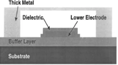
[image:2.612.61.291.151.278.2]RF MEMS is the attractive field for both scientific research and industries due to their application in military wireless communication, remote controlling and sensing system.
Fig. 1 Air Bridge MEMS switch Table. 1 Scope of MEMS
Frequency range Bandwidth (GHz)
Radar systems for defence application
5-94
Satellite communication 12-35
Wireless communication 0.8-6
Instrumentation system 0.01-50
Applications
The high tunable and cheap communication[9][12] system consume minimum amount of power and large bandwidths for high data rates, micromachining techniques and MEMS devices are used in different field of applications. The significant idea in RF MEMS are[8, 13] miniature of mechanical devices and physical movements are achieved by the function of microwave switch or variable capacitor. RF MEMS switches with figure-of-merit cut-off frequency of 30-80THZ that is 100 times better than GaAs transistor.
Objective
The objective of the work is,
To reduce the size of RF MEMS switches
To optimize the range of RF signals, that purpose such filter, oscillator and switches in micro machined devices
To realize the MEMS switches device low power consumption, less insertion loss and high isolation
Organization
The remaining section of this paper is arranged as follows: Section II deliberates the detailed representation of the related works for the existing RF-MEMS design process and filtering applications. Section III elaborate the description of proposed Filtering technique and RF MEMS design layout. Section IV illustrates the performance comparison of proposed with
traditional filtering techniques. Section V discusses conclusion and the work could be done on future with the proposed work.
II. RELATED WORKS
In this section, the traditional FET layout design utilized the RF MEMS and their filter applications are reviewed with its advantages and disadvantages.[14] reviewed the MEMS technology for human centered application in both healthcare, physical actions. The sensing tools were offered the innovative and integrated solutions for some specific application.
[19] designed and fabricated the radio frequency (RF) micro-electro-mechanical system (MEMS) switches for smart antenna applications. A metal electro thermal actuator was used to derive the switches that were capable to made large displacement and high contact force at lower temperature. 8
displacement was achieved by parallel beam actuator and MEMS switches. RF performance was improved by suspending the switching structures 25 above the substrate so it was also reduce the losses in substrate. The developed MEMS switches were offered the good performance. [20] presented a compact radio frequency micro electro menchanical system switch on quartz substrate. By combining two membranes in serious and shunt configuration on single substrate was achieved the high isolation and it was maintaining the compactness of switch dimensions. The cavity was designed by ohmic and capacitive switch membrances over the co-planar waveguides on substrate. The finite element modeler was analyzed and calculated by using spring constant, pressure distribution, pull in voltage, Q-factor, R, L and C. Biasing pads were offered on both ends of switch for electrostatic actuation. The same voltage level was designed and optimized by membrane with low spring constant. [21] proposed the radiating pattern reconfigurable antenna by using RF micro electro-mechanical system (RF MEMS) switches. The merit of the antenna was low profile, and small size. It was included with one main patch, two assistant patches, and two RF MEMS switches. This method was verified by the planner antenna with pattern reconfiguration characteristics. Three reconfigurable patterns were obtained by RF MEMS switches. The small size and lightweight characteristics of an excellent candidate for satellite searching, tracing and communication system. [22] analyzed the performance of capacitive RF MEMS switches. The fabricated switches were measured in up and down states and it was observed the impact of RF performance of different geometric parameters and fabrication process. The cycling tests were evaluated by using reliability of fabricated RF MEMS switches under bipolar voltage excitation. The switches were properly modified as,
The geometric parameters of bridge
The presence or absence of floating metal on actuator
The suspended or fixed bridge on the actuator
The isolation switches with different geometric parameters of bridge was measured and modeled to obtain the tuning of resonance frequency from 23 GHz to 30GHz. [23] presented the high power and reliable radio frequency (RF) micro-electro-mechanical system switches with single pole single throw (SPST) and single pole triple throw (SP3T) configuration. A simple standard silicon-on-insulator process was made by using an in-plane movable structure with a single layer. SPST switch was achieved the uniform current distribution each contact and also increased the power handling capability of switches. A separate individual actuations were derivate by SP3T switch. The over coated on contact area of switches to reduce the resistance loss on material and contact points. The switches were applied in
wireless communication. [24] designed and fabricated the sub millimeter wave 500-750GHz MEMS waveguide switch comprising a MEMS reconfigurable surface of blocking or unblocking the wave propagation via waveguide. The low insertion loss in non-blocking state and high isolation in blocking state were achieved by design parameter. The ohmic contact waveguide switch was not work properly in blocking state and isolation was achieved only 5db. The life time measurement was achieved the high actuator reliability at medium actuation voltage with 100 million cycles. [25] suggested the design methodology for extremely improved the hot switching reliability of contact type radio frequency micro-electro-mechanical (RF MEMS) switches. The parallel with low resistance contacts was significantly reduced the electric filed and also reduced the contact degradation associated with the field of induced material transfer. A novel mechanical scheme was designed to allow the accurate protection actuation order to be realized by using single actuator and bias electrode. The drawback of the work was the structural design and contact materials were required to improve the hot-switching lifetime.
III. PROPOSED WORK
Fig. 2 Overall flow diagram Parameter initialization
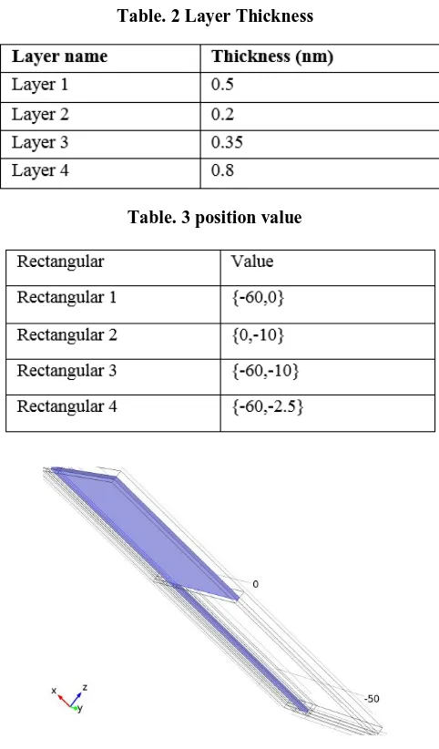
An Initial, the RF MEMS is create based on the exact measurement for each and every layer. It includes 3 layers and various materials are located in each layer. The design layout is showed in Fig 3, that dimensionality levels are analyzed based on rules of circuit designing. Also, some dimension levels are followed in entire design of each layer. The selection of material is marked like a box shape.
Fig. 3 Parameter initialization
Fig 3 represents the parameter initialization for designing process and it includes four layers. The position of the material is placed among the 0 to -60. The thickness of each
layer measured in nanometer (nm). The distance of each layer is {1, 2, and 4}
[image:4.612.50.296.41.408.2]Table. 2 Layer Thickness
Table. 3 position value
[image:4.612.316.557.86.497.2]Fig. 4 Si poly silicon material
Fig 4 shows the selection of Si poly silicon material. Here the domains are selected with the range of 8, 20, 35, 47, 50, and 53. The density and young’s modulus are measured
inters of and . The poisson’s ratio of
[image:4.612.74.287.534.668.2]Table. 4 parameter description
Table. 5 Si poly silicon material
Selecting material
After designing the layout design, various materials are placed in each and every layer. Material selection is the process for analyzing the characteristics for desired performance which is based on their attributes like mechanical, electrical. The material selection chart represents the each axis and their material property during the analyzing process of material selection. The designing components are specified with three parameters like functional property, geometric property and material property. Here the silicon and air material are used for entire design. Because it reduced the cost and improve the efficiency of entire circuit.
(1)
(2)
[image:5.612.316.555.77.439.2]Fig. 5 Bridge Selection
Table. 6 selection of basic values
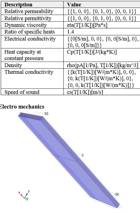
Electro mechanics
Fig. 6 Electromechanical design
Here, the dimension of the material is selected as the domain range of 1-54.
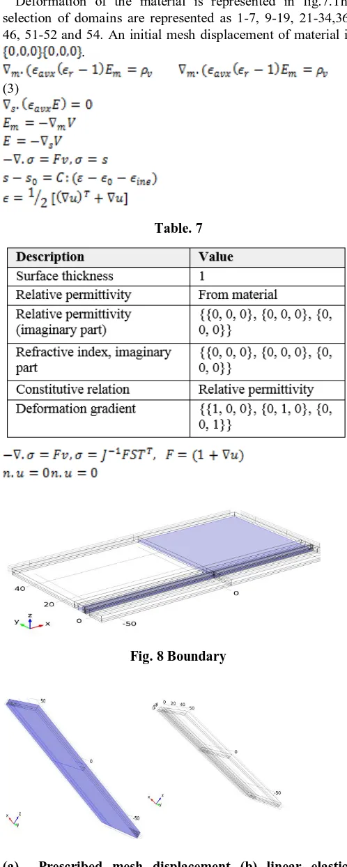
Deformation of the material is represented in fig.7.The selection of domains are represented as 1-7, 9-19, 21-34,36-46, 51-52 and 54. An initial mesh displacement of material is
.
[image:6.612.45.294.56.678.2](3)
Table. 7
Fig. 8 Boundary
[image:6.612.200.546.127.775.2](a) Prescribed mesh displacement (b) linear elastics Dielectric
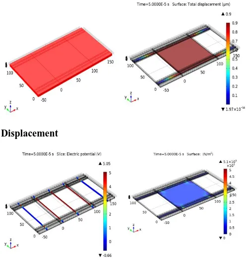
Fig. 9 Displacement
Filter design
The comb line band pass filter is included with an array of coupled resonators and it included with line elements from 1 to n. every resonator line elements are placed in ground and also the capacitor is loaded among the other end. The coupled line element of 0 and n+1 are both input and output but they are not considered as resonator. If the capacitor is not offer, then the resonator lines are long at their distance. The line elements are created from TEM mode transmission line like strip line.
The larger loading capacitance, the shorter resonator lines that are more compact filter design with wider stop band among their initial pass band and second pass band. The lumped capacitors are offered the convenient means for filter tunning that are required the particular for their narrow band filters.
Filter is constructed based on chosen ladder type of low pass prototype with their parameter for
. The resonator susceptance parameter
(4)
Here, terminating line admittance
Middle band electrical length of resonator Interpreted physically as admittance of line with
adjacent lines grounded.
The choice of represents the admittance level in filter and it influence the unloaded quality elements of their resonator. The fractional bandwidth (FBW),
(5)
(6)
The lumped capacitance are,
(7)
Here,
IV. PERFORMANCE ANALYSIS
[image:7.612.56.295.163.285.2]In this section, the experimental results of both existing and proposed filter design with the support of RFMEMS. These techniques are evaluated based on their displacement and capacitor. In this evaluation, the COMSOL tool is used to design the filter for communication application.
Table. 8 characteristics of proposed design
[image:7.612.323.547.203.342.2]The tool is used to design the RF MEMS layout and also generate the library.
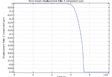
[image:7.612.68.260.319.451.2]Fig. 10 Displacement of center device and function time
Fig 10 represents the displacement of center device and their function time of proposed layout design, where the x-axis represents the time (s), and y-axis represents the displacement, field (z) and compound . It analyzed that the time is decreased with the increase in the displacement filed. The overall time is increased to 4ms in designed layout. The displacement is mainly calculated based on their time period. Also, it estimates the overall current value of the circuit.
Fig. 11 Capacitance
Fig 11 represents the capacitance value of proposed design layout. In graphical representation, the axis represents the capacitance in and axis represents the time in seconds. The time period is varied from and the capacitance value is
varied from . The time
period is 0 to 3s at the capacitance value of 1F. The time
period is suddenly increased from 1.5F to .
Filter design
Fig. 12 global: Absolute value of admittance(S)
[image:7.612.326.544.473.609.2]Fig 12 shows the global: Absolute value of admittance. In graphical representation, the y- axis represents the absolute value of admittance and y-axis represents the frequency in Hz. The frequency values are randomly in varied with different absolute value of admittance in seconds. The frequency values are mostly used in Ka band for larger communication.
Fig. 13 Quality factor
Fig 13 shows the quality factor for proposed design layout. Here the y-axis represents the quality factor and x- axis shows the frequency. It varies from 2.15 to
Hz. The quality factor is increased upto 1200 for 2.25Hz. After that, the
[image:7.612.58.278.599.723.2]Simulation results
COMSOL is a user interface, it offers the complete and integrated environment for physics modeling and simulation design applications. It have quick access toolbar and information windows have nongraphic information like messages, progress, log, table and external process.
Displacement
[image:8.612.46.294.180.458.2](b) Electric displacement (c) Contact force
Fig. 14 Simulation Results V. CONCLUSION
In the proposed section, a RF MEMS switch was designed by the initialization of parameters like size, height, width, length, and the thickness. The selection of material was carried out. Mostly, the selection of material will be a silicon and air as silicon was the semiconducting material. By using the boundary, domain, edge, vertices of edges the configuration might be analyzed. This process was carried followed by the displacement mechanism. The RF switch was utilized in the filter circuit for the extraction of filtered results. Then the performance analysis is made thus comparing the existing methodologies with the proposed method. From the result, it was evident that the proposed methodology performs well than the existing methodologies.
REFERENCES
1. M. Angira and K. Rangra, "Design and investigation of a low insertion loss, broadband, enhanced self and hold down power RF-MEMS switch," Microsystem technologies, vol. 21, pp. 1173-1178, 2015. 2. D. Shojaei-Asanjan and R. R. Mansour, "The Sky's the Limit: A
Switchable RF-MEMS Filter Design for Wireless Avionics Intracommunication," IEEE Microwave Magazine, vol. 18, pp. 100-106, 2017.
3. A. Hald, J. Seelhorst, M. Reimann, J. Scheible, and J. Lienig, "A novel polygon-based circuit extraction algorithm for full custom designed MEMS sensors," in Synthesis, Modeling, Analysis and Simulation Methods and Applications to Circuit Design (SMACD), 2016 13th International Conference on, 2016, pp. 1-4.
4. M. Weyers and G. Erbert, "System for frequency conversion, semiconducting device and method for operating and manufacturing the same," ed: Google Patents, 2015.
5. A. Vasiliev, A. Pisliakov, A. Sokolov, N. Samotaev, S. Soloviev, K. Oblov, et al., "Non-silicon MEMS platforms for gas sensors," Sensors and Actuators B: Chemical, vol. 224, pp. 700-713, 2016.
6. G. S. Wood, C. Zhao, S. H. Pu, I. Sari, and M. Kraft, "An Investigation of Structural Dimension Variation in Electrostatically Coupled MEMS Resonator Pairs Using Mode Localization," IEEE Sensors Journal, vol. 16, pp. 8722-8730, 2016.
7. Y. Liu, Y. Bey, and X. Liu, "High-power high-isolation RF-MEMS switches with enhanced hot-switching reliability using a shunt protection technique," IEEE Transactions on Microwave Theory and Techniques, vol. 65, pp. 3188-3199, 2017.
8. Z. Chen, W. Tian, and X. Zhang, "Effect of surface asperities on the capacitances of capacitive RF MEMS switches," Journal of Micromechanics and Microengineering, vol. 27, p. 034002, 2017. 9. S. Molaei and B. A. Ganji, "Design and simulation of a novel RF
MEMS shunt capacitive switch with low actuation voltage and high isolation," Microsystem Technologies, vol. 23, pp. 1907-1912, 2017. 10. R. R. Benoit and N. S. Barker, "Superconducting tunable microstrip
gap resonators using low stress RF MEMS fabrication process," IEEE Journal of the Electron Devices Society, vol. 5, pp. 239-243, 2017. 11. M. Pustan, C. Birleanu, C. Dudescu, R. Chiorean, R. Muller, and A.
Baracu, "Design, fabrication and characterization of RF MEMS switches with robust contact," in Design, test, integration and packaging of MEMS/MOEMS (DTIP), 2017 symposium on, 2017, pp. 1-6.
12. Z. Zhou, W. Nie, Z. Xi, and X. Wang, "A High-Electrical-Reliability MEMS Inertial Switch Based on Latching Mechanism and Debounce Circuit," SENSORS, vol. 13441, p. 1, 2015.
13. S. Shekhar, K. Vinoy, and G. Ananthasuresh, "Design, fabrication and characterization of capacitive RF MEMS switches with low pull-in voltage," in Microwave and RF Conference (IMaRC), 2014 IEEE International, 2014, pp. 182-185.
14. G. Ciuti, L. Ricotti, A. Menciassi, and P. Dario, "MEMS sensor technologies for human centred applications in healthcare, physical activities, safety and environmental sensing: a review on research activities in Italy," Sensors, vol. 15, pp. 6441-6468, 2015.
15. Y. Hui, J. S. Gomez-Diaz, Z. Qian, A. Alù, and M. Rinaldi, "Plasmonic piezoelectric nanomechanical resonator for spectrally selective infrared sensing," Nature communications, vol. 7, p. 11249, 2016.
16. H. Samaali, B. Ouni, and F. Najar, "Design and modelling of MEMS DC–DC converter," Electronics Letters, vol. 51, pp. 860-861, 2015. 17. A. K. Ilkhechi, H. Mirzajani, E. N. Aghdam, and H. B. Ghavifekr, "A
novel electrostatically actuated spdt rotary RF MEMS switch for ultra-broadband applications," in Electrical Engineering (ICEE), 2015 23rd Iranian Conference on, 2015, pp. 1175-1179.
18. H. Jaafar, K. Beh, N. A. M. Yunus, W. Z. W. Hasan, S. Shafie, and O. Sidek, "A comprehensive study on RF MEMS switch," Microsystem technologies, vol. 20, pp. 2109-2121, 2014.
Technologies, vol. 21, pp. 487-495, 2015.
20. T. Singh, "Design and finite element modeling of series-shunt configuration based RF MEMS switch for high isolation operation in K– Ka band," Journal of Computational Electronics, vol. 14, pp. 167-179, 2015.
21. Z. Deng, X. Guo, H. Wei, J. Gan, and Y. Wang, "Design, analysis, and verification of Ka-band pattern reconfigurable patch antenna using RF MEMS switches," Micromachines, vol. 7, p. 144, 2016.
22. A. Persano, F. Quaranta, G. Capoccia, E. Proietti, A. Lucibello, R. Marcelli, et al., "Influence of design and fabrication on RF performance of capacitive RF MEMS switches," Microsystem Technologies, vol. 22, pp. 1741-1746, 2016.
23. J. Pal, Y. Zhu, J. Lu, D. Dao, and F. Khan, "High power and reliable SPST/SP3T RF MEMS switches for wireless applications," IEEE Electron Device Letters, vol. 37, pp. 1219-1222, 2016.
24. U. Shah, T. Reck, H. Frid, C. Jung-Kubiak, G. Chattopadhyay, I. Mehdi, et al., "A 500–750 GHz RF MEMS Waveguide Switch," IEEE Transactions on Terahertz Science and Technology, vol. 7, pp. 326-334, 2017.
25. Y. Liu, Y. Bey, and X. Liu, "Extension of the hot-switching reliability of RF-MEMS switches using a series contact protection technique," IEEE Transactions on Microwave Theory and Techniques, vol. 64, pp. 3151-3162, 2016.
26. Y. S. Mehrabani and M. Eshghi, "Noise and Process Variation Tolerant, Low-Power, High-Speed, and Low-Energy Full Adders in CNFET Technology," IEEE Transactions on Very Large Scale Integration (VLSI) Systems, vol. 24, pp. 3268-3281, 2016.