Abstract:Now the era is of electronic gadgets like processors and portable devices, in which Memory plays a significant role through the usage of Static RAMs (SRAMs).Hence designing of Low power SRAM is immense for applications. But the design of SRAM is involved in higher power requirement. So there is still scope for adequate Low power Memory Array design. The Main Moto of this paper is involved in designing & Simulating Low Power 16x16 SRAM Arrays using 7T SRAM cells based on Conventional, Self Controllable Voltage (SVL) & Improved Self Controllable Voltage (I-SVL) methods. Also Comparative Power and SNM Analysis is carried between Conventional 7T, 7T-SVL and 7T-ISVL based Arrays. The Proposed Array using 7T Cell consumes 6.24mW which is 67.64% lesser than the Array design [2].Also I-SVL based 7T SNM is better than the SVL-7T and 7T based cell.The proposed work is carried using cadence virtuoso tool with standard library gpdk 180nm.Also Proposed Array based on I-SVL is efficient in terms of power. The proposed Cell SNM resulted in 68.57% higher in comparison with existing cell of 8T and 10T [3].
Keywords : SRAM, Improved – Self Controllable Voltage level (I-SVL), Self Controllable Voltage level (SVL).
I. INTRODUCTION
In Current trend, less power and low delay SRAMs are the discriminating parts of various VLSI chips. This is specifically applicable for microchips, in which built up chip areas are improving to enhance the increasing demands to speed the cache memory and processor. SRAM is applicable as Cache memory due to quick operation and used in performing the assignment of Microprocessor and memory interface. Due to rapid growth in the advanced technologies of VLSI fabrication, the operation speed of the Boolean logic gates is increased but comparatively the memory array speed is not yet enhanced.
With the advancement in technology through portable handheld devices, always there is demand for large amount of data storage. This can be achieved through low power and high package density. System on Chip (SOC) design helps in achieving the above stated criteria at low cost [1]. Static-RAM (SRAM) is the major block of SOC design that helps in storing larger data information. Also SRAM is the significant component in cache memory of Microprocessor, Microcontroller and portable devices resulting in higher speed and lower power operation [2].Normally SRAM is built using latch circuit, which has 2 stable states ‘0’ & ‘1’ with information visible until power is made available.
Revised Manuscript Received on September 03, 2019
Hemanth Kumar C S*, Department of Electronics & Communication Engineering, Government Engineering College, Ramangara, India, Research scholar VTU Belgaum. Email: [email protected]
Kariyappa B S, Department of Electronics & Communication Engineering, RVCE,Bengaluru,India.Email: [email protected]
DRAM requires periodic refreshing which is absence in case of SRAM [3].
The Outline of paper is depicted by the five sections with the inclusion of introduction. Section II is about the related work so far.Section III provides the information about SRAM Array. Section IV exhibits Design, implementation and simulation of SRAM Memory Arrays. Section V describes simulation outcomes and their discussions. Last section reflects about the conclusion of the research work carried.
II. RELATEDWORK
The work proposed in [1], [4] is about discussing the design & implementation of 16X16 SRAM Array to store 256 bits. The proposed array [1] is built using Conventional 6T SRAM Cell.The work carried in [2] demonstrates the design of 16x16 SRAM based Array on Conventional 7T SRAM Cells.[5]Proposes the design and implementation of 16X16 SRAM Array employing I-LSVL Method.
In each of the proposed methods Memory array is built using Peripherals like Sense amplifier, Row – Column decoder, Pre charge circuit. The design of sense amplifier in [1] is using differential type and where as in [5] employing Current mirror with single ended output. In each of the proposals the total array power is evaluated employing Cadence Virtuoso tool using Generic process design kit(gpdk) 180nm technology. In the present context of the work the comparative power analysis of 16x16 SRAM Array is carried with basic 7T, 7T-SVL, and 7T-ISVL.
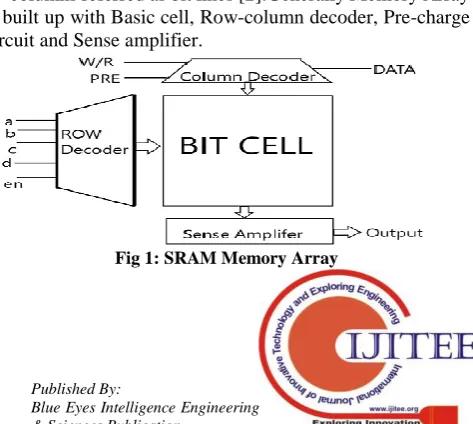
[image:1.595.313.550.617.829.2]III. SRAMMEMORYARRAYSTRUCTURE Fig 1 describes about the Memory array using SRAM cells. Single row of the proposed designed memory array has 16 cells further these 16 rows of 16 cells are used to form 16X16 SRAM Array[4].Individual SRAM cell in each row of 16X16 SRAM Array is arranged in the form of horizontal rows and vertical columns, accessed via row and Column decoder. In general SRAM Array has 2N rows called as word lines and 2M columns referred as bit lines [2].Generally Memory Array is built up with Basic cell, Row-column decoder, Pre-charge circuit and Sense amplifier.
Fig 1: SRAM Memory Array
7T Based SRAM Topologies with Low Power
and Higher SNM
IV. DESIGNANDIMPLEMENTATION
A. 7T SRAM
The basic 7T SRAM cell is illustrated in fig2. The 7T SRAM cell made up of two pull up, two access and three pull down transistors. Word input line is used in enabling or disabling the cell. The data intend to write or read is fed through bl and
[image:2.595.317.538.78.289.2]blb lines. Output ports q and qb are involved in obtaining intermediate outputs
.
Fig 2: Basic 7T SRAM Cell
B. SVL BASED 7T SRAM
SVL based 7T SRAM Cell is shown in fig 3.Self Controllable Voltage Level (SVL) technique is applicable in reduction of leakage power at standby mode. In SVL method both USVL and LSVL is placed at upper and lower portion of basic 7T SRAM cell [5].A provision is made in standby mode to supply lower and higher VDD voltage across load using Switch.
Fig 3: SVL based 7T SRAM Cell
C. PROPOSED I-SVL BASED 7T SRAM
I-SVL technique is applicable in reducing stand-by power drastically and maintains the high speed performance. During active mode of SRAM operation, I-SVL switch provides higher supply and lesser ground voltage to SRAM, so it can operate quickly. On the other side during standby mode I-SVL supplies slightly lesser supply voltage and larger ground level voltage. Thus I-SVL switch is meant in decreasing gate leakage current during stand by operation.
[image:2.595.55.284.144.370.2]Proposed I-SVL employed 7T SRAM Cell configuration discussed above is depicted in fig4.
Fig 4: Proposed I-SVL based 7T SRAM Cell.
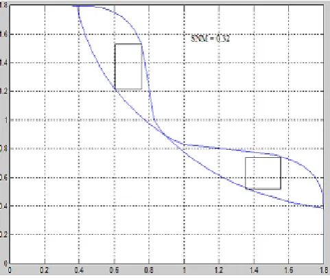
D. STATIC NOISE MARGIN
The Stable nature of an SRAM Cell is decided by the concept of Static noise margin. The higher Noise range sustained by an SRAM Cell without altering the written data across a node is measured through SNM. Generally larger SNM indicates the better performance of the SNM circuit. SNM is a key factor for measuring the performance at the time of holding and read operations. Also its data changes depending on the required exact operation mode. SNM is evaluated in two ways. One way is graphical method of creating butterfly curve with the Voltage Transfer Characteristics (VTC).The VTC curve is generated using the DC Analysis by plotting the output with respect to input. The DC Plot is drawn for the cross coupled inverters and Combined to obtain SNM. The SNM is calculated by the length of highest square which is fitted between the lobes of the two curves. The below fig depicts the SNM of different 7T SRAM Cell Topologies.
[image:2.595.48.277.495.646.2] [image:2.595.307.548.523.727.2]Fig 6: SNM of SVL Based 7T SRAM
[image:3.595.47.283.67.584.2]Fig 7: SNM of I-SVL Based 7T SRAM
[image:3.595.312.543.267.503.2]Fig 8: Bar chart comparison of SNM of different 7T SRAM Cell Topologies
Table 1: SNM Comparison
Cells 7T Work
3[3][8 T & 10T]
7T-SV L
Propose d 7T-ISV L
% Increm ent
SNM( Volts)
0.32 0.49 0.7686 0.826 68.57
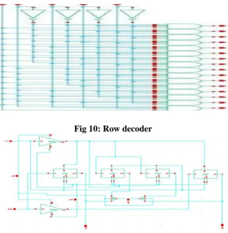
E. ARRAY PERIPHERALS
Before carrying the array design one has to take care about designing of array peripherals namely Sense amplifier, Row & Column decoders. The simulation is carried using Cadence
[image:3.595.311.545.575.724.2](Version 6.1.4).The technology file included for simulation is gpdk 180.
Fig 9: Sense Amplifier via Current mirror with single ended output configuration.
Fig 10: Row decoder
Fig 11: Column Decoder
F. Array Design
Array design involves in combining the above designed peripherals in proper order to achieve 16x16 SRAM based memory array. It is capable of holding 256 bits.
Fig 12: 16x16 SRAM based Array employing I-SVL 7T SRAM 0
0.1 0.2 0.3 0.4 0.5 0.6 0.7 0.8 0.9
7T Work3 SVL-7T ISVL-7T SNM Comparison
[image:3.595.57.278.616.740.2]V. SIMULATION OUTCOMES
Section V explains about the simulation results of 16x16 SRAM based Array employing Conventional 7T SRAM Cell, SVL 7T SRAM Cell and I-SVL 7T SRAM Cell.The proposed work is designed and simulated using Cadence Spectre Virtuoso tool. The transient simulation outcome of 16x16 SRAM based Array with respect to read and write operation on 1st row (address input to decoder is ‘0000’)using basic 7T,SVL 7T,I-SVL 7T SRAM Cell is shown in fig 14,15 & 16 respectively.
[image:4.595.312.538.49.220.2]Fig13: Address to row decoder ‘0000’ to enable 1st row
Fig 14: Transient output of Read & Write operation in 16x16 SRAM based Array employing Conventional 7T SRAM Cell.
Fig 15: Transient output of Read & Write operation in 16x16 SRAM based Array employing SVL 7T SRAM Cell
Fig 16: Transient output of Read & Write operation in 16x16 SRAM based Array employing I-SVL 7T SRAM Cell.
From the simulation outcome it is clear that store (write) operation is enabled by forcing w_r input to high (‘1’) ,Pre input to high(‘1’) and data to be stored(written) is fed at input data. The store (write) operation output of logic ‘1’ & ‘0’ is available at Sense amplifier outputs (S0-S15) based on the row enabled. Store ‘1’ and ‘0’ operation results on 1st Row (Row decoder input ’0000’) are indicated in figs 13, 14, 15 & 16 respectively.
Read operation is enabled by making w_r input to low (’0’), pre input to high (’1’) and data to be accessed (read) are available at sense amplifier outputs (S0-S15) based on the row enabled. The accessing (read) ‘1’ and ‘0’ operations on 1st Row (Row decoder input ’0000’) are indicated in figs 13, 14, 15 & 16 respectively.
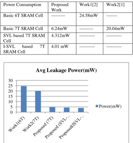
[image:4.595.312.542.478.726.2]The power consumption of various 16x16 SRAM Array using basic 7T, SVL based 7T & I-SVL employed 7T SRAM Cell is tabulated in table 1.
Table 2: Comparison of 16x16 SRAM Array in terms of Power
Power Consumption Proposed Work
Work1[2] Work2[1]
Basic 6T SRAM Cell --- 24.58mW ---
Basic 7T SRAM Cell 6.24mW --- 20.04mW SVL based 7T SRAM
Cell
4.312mW --- ---
I-SVL based 7T SRAM Cell
4.01 mW --- ---
Fig 17: Bar Chart of Power Consumption in16x16 SRAM Array
0 5 10 15 20 25 30
Avg Leakage Power(mW)
[image:4.595.56.280.550.736.2]Author-1 Photo VI. CONCLUSION
Different SRAM Arrays of size 16X16 is designed and capable of storing 256bits.These arrays were designed using peripheral components like Row & Column decoder, Precharge circuit, Sense amplifier. In this proposed work 16X16 SRAM Arrays are designed using Conventional 7T, 7T-SVL & 7T-ISVL cells. The proposed work is simulated using cadence virtuoso standard library gpdk 180nm.The comparative power analysis is made between the arrays and compared the same with the previous works. The proposed array using 7T cell consumes 6.24mW which is 67.64% lesser than the existing Array design [2].Also Proposed SRAM Array using 7T-ISVL consumes lesser power in comparison with 7T & 7T-SVL based cell.The proposed 7T based on ISVL shows 68.57% incremented value of SNM in par with existing cell of 8T and 10T [3].Also the proposed ISVL based 7T SRAM cell has higher SNM in comparison with Conventional 7T and SVL based 7T SRAM cell.
REFERENCES
1. Rashmi Bisht, Priyanka Agarwal, Pooja Karki, Peyush Pande, “Low Power and Noise Resistant 16X16 SRAM Array Design using CMOS Logic and Differential Sense Amplifier” in
ICCCA2016,978-1-5090-1666,IEEE 2016.
2. Rashmi Bisht, Ashutosh Pranav,” Design of 16X16 SRAM Array Using 7T SRAM Cell for Low Power Applications” Journal of Graphic Era University, Volume 5,Issue 2,2017.
3. Himanshu Banga, Dheeraj Agarwal ,“ Single Bit -Line 10T SRAM cell for Low power and High SNM”, Proceeding of International conference on Recent Innovations isSignal Processing and Embedded Systems (RISE -2017),978-1-5090-4760-4,IEEE 2017.
4. Divyesh Sachan, Harish Peta, Kamaldeep Singh Malik, Manish Goswami, ”Low Power Multi Threshold 7T SRAM Cell”, International MidwestSymposiumonCircuitsandSystems(MWSCAS),978-1-5090-09 16-9,IEEE 2016.
5. Hemanth Kumar CS, Kariyappa B.S,” Design and Power Analysisof16x16SRAMArrayEmploying7TI-LSVL”,Internationalconfe renceonRecenttrendsinElectronics,Information&CommunicationTechn ology(RTEICT2018),978-1-5386-2440-1,IEEE 2018.[Yet to Publish] 6. Preeti S Bellerimath, R.M Banakar”Implementation of 16X16 SRAM
Memory Array Using 180nm Technology”, International Journal of Current Engineering and Technology ,NCMSE 2013,ISSN 2277-4106. 7. Hemanth kumar CS, Kariyappa B S,” SRAM Design Using Memristor
and Self-controllable Voltage (SVL) Technique”, Proceedings of International Conference on Computational Intelligence and Data Engineering, Lecture Notes on Data Engineering and Communications Technologies,978-981-10-6319-03,Springer 2018.
8. Hemanth Kumar C S, Kariyappa B S,” Analysis of Low Power 7T SRAM Cell Employing Improved SVL (ISVL) Technique”, International Conference on Electrical, Electronics, Communication, ComputerandOptimizationTechniques(ICEECCOT),978-1-5386-2361-9,IEEE 2017.
9. Basavaraj Madiwalar, Kariyappa B.S,”Single Bit Line 7T SRAM Cell for Low Power and High SNM”, International Multiconference on Automation, Computing, Control, Communication and Compressed Sensing (IMAC4S-13), 978-1-4673-5089-1, IEEE 2013.
10. Gauravvashist,HiteshPahuja,BalwinderSingh,SudhakerPandey, ”Design and Comparative analysis of Low power 64 bit SRAM and its Peripherals using Power Reduction Techniques”,5th International
Conference on Wireless networks & Embedded Systems(WECON), 978-1-5090-0893-3,IEEE 2016.
11. BabakMohammadi, oskarandersson, joseph Nguyen,”A 128Kb 7T SRAM using a single cycle boosting mechanism in 28nm FD-SOI,IEEE Transactionsoncircuits& systems-I ,10.1109/TCSI.2017.2750762,2018. 12. Shourya Gupta,Kirti Gupta,Neeta Pandey,”32 nm sub threshold 7T SRAM bit cell with Read assist”,IEEE Transactions on Very large scale Integration(VLSI) systems, 10.1109/TVLSI.2017.2746683,December 2017.
13. Kazi Fatima Sharif, Riazul Islam et all,” 7T SRAM based Memory Cell”, International Conference on Innovative Mechanisms for Industry Applications (ICIMIA),978-1-5090-5960-7/2017.
14. Sakshi Saxena1, Shipra Mishra,”Analysis of Leakage Current and SNM for 7T SRAM Cell in Nanometre Era”,IJRTER 2016.
15. Pinki Narah, Mrs. Sharmila Nath,” A Comparative Analysis of SRAM Cellsin45nm,65nm,90nmTechnology”,IJERA2018,10.9790/9622-0805 013136.
AUTHORSPROFILE
Mr Hemanth Kumar C S working as Assistant Professor in Dept. of E&C, Government Engineering College, Ramangara, Bengaluru. Presently Research scholar at RVCE Bengaluru, VTU, Belgaum. He has 12 years of Teaching Experience and published papers in International Journals and conferences. His Publications are cited in Scopus and Google Scholar. His areas of interest are VLSI Design and Embedded Systems.