This is a repository copy of
Temperature study of Al0.52In0.48P detector photon counting
X-ray spectrometer
.
White Rose Research Online URL for this paper:
http://eprints.whiterose.ac.uk/107003/
Version: Accepted Version
Article:
Butera, S., Gohil, T., Lioliou, G. et al. (2 more authors) (2016) Temperature study of
Al0.52In0.48P detector photon counting X-ray spectrometer. Journal of Applied Physics,
120 (17). 174503. ISSN 0021-8979
https://doi.org/10.1063/1.4966940
[email protected] https://eprints.whiterose.ac.uk/ Reuse
Unless indicated otherwise, fulltext items are protected by copyright with all rights reserved. The copyright exception in section 29 of the Copyright, Designs and Patents Act 1988 allows the making of a single copy solely for the purpose of non-commercial research or private study within the limits of fair dealing. The publisher or other rights-holder may allow further reproduction and re-use of this version - refer to the White Rose Research Online record for this item. Where records identify the publisher as the copyright holder, users can verify any specific terms of use on the publisher’s website.
Takedown
If you consider content in White Rose Research Online to be in breach of UK law, please notify us by
Temperature study of Al
0.52In
0.48P detector photon counting
X-ray spectrometer
S. Butera1a), T. Gohil1, G. Lioliou1, A. B. Krysa2, A.M. Barnett1
1
Semiconductor Materials and Device Laboratory, School of Engineering and
Informatics, University of Sussex, Brighton, BN1 9QT, UK.
2
EPSRC National Centre for III-V Technologies, University of Sheffield, Mappin
Street, Sheffield, S1 3JD, UK.
A prototype 200 m diameter Al0.52In0.48P p+-i-n+ mesa photodiode (2 m i-layer) was
characterised at temperatures from 100 °C to -20 °C for the development of a
temperature tolerant photon counting X-ray spectrometer. At each temperature, X-ray
spectra were accumulated with the AlInP detector reverse biased at 0 V, 5 V, 10 V
and 15 V and using different shaping times. The detector was illuminated by an 55Fe
radioisotope X-ray source. The best energy resolution, as quantified by the full width
at half maximum (FWHM) at 5.9 keV, was observed at 15 V for all the temperatures
studied; at 100 °C a FWHM of 1.57 keV was achieved, this value improved to 770 eV
FWHM at -20 °C. System noise analysis was also carried out and the different noise
contributions were computed as functions of temperature. The results are the first
demonstration of AlInP’s suitability for photon counting X-ray spectroscopy at
temperatures other than ≈ 20 °C.
I. INTRODUCTION
Al0.52In0.48P is a III-V semiconductor that has recently started to receive attention for
the development of photon counting X-ray spectrometers; at room temperature,
non-avalanche [1] and non-avalanche photodiodes [2] have been shown to be sensitive to
X-ray photons from 55Fe radioisotope X-ray sources. Such systems have been shown to
have energy resolutions of 930 eV and 682 eV, respectively, at room temperature [1,
2]. Due to its wide indirect bandgap (2.31 eV [3]), Al0.52In0.48P is expected to be
useful for building high-temperature tolerant X-ray spectrometers that can be
beneficial in many applications including space missions and terrestrial applications
outside the laboratory environment. Furthermore, Al0.52In0.48P is expected to have a
reduced likelihood of damage from radiation and has been shown to present lower
thermally-generated leakage currents than alternative narrow and wide bandgap
materials (e.g. Silicon and AlGaAs) allowing operation at room temperature and
above without cooling systems [4, 5], potentially this may result in cost savings due to
reduced mass, volume and power requirements for such instruments. Because of its
good linear attenuation coefficients as a consequence of the presence of Indium
(atomic number 49), Al0.52In0.48P has also higher X-ray quantum efficiency per unit
thickness [1] compared to those of some other wide bandgap X-ray photodetectors,
e.g. SiC, AlGaAs and GaAs [6, 7]. Moreover, it is nearly lattice matched with GaAs
and the crystalline quality of the resultant material can be very high in comparison to
III-V nitrides, IV and II-VI compounds of a similar bandgap. With respect to II-VI
compounds, Al0.52In0.48P also does not have disadvantages such as weakness of the
crystalline lattice, which often results in high concentration of dislocation and native
defects, and doping control problems in other materials [8].
All these properties make Al0.52In0.48P a promising candidate material for the
production of robust, compact and high-energy resolution X-ray spectrometers that
can work over a broad range of temperatures.
X-ray photon counting spectroscopy at high temperatures has been previously
reported using different wide bandgap semiconductor detectors made from materials
such as SiC, Al0.8Ga0.2As, and GaAs. A SiC X-ray detector was demonstrated by
Bertuccio et al. [9] with an energy resolution (FWHM) at 5.9 keV of 233 eV at 100
°C; whilst an Al0.8Ga0.2As photodiode was reported by Barnett et al. [10] with energy
resolution at 5.9 keV of 2.2 keV at 90 °C, limited by the noise of the preamplifier
used. GaAs structures were also developed and characterised for use as X-ray
spectrometers by Barnett et al. [11] and Lioliou et al. [12] with energy resolutions at
5.9 keV of 1.5 keV at 80 °C, and 840 eV at 60 °C, respectively. Other materials
commonly considered for use at high temperatures for the detection of soft and hard
X-rays, as well as -rays, include CdTe and its related compounds (e.g. CdZnTe,
CdMnTe) [13]. At 92 °C, a FWHM at 122 keV of 53 keV was observed for CdTe
[14]; whilst at 70 °C, a FWHM at 32 keV of 9.4 keV was reported for CdZnTe [15].
choices for producing large area [16] and thick radiation detector, with adequate
efficiency to high energy X- and -rays; spectroscopic CdZnTe and CdTe detector
imaging arrays, for example, have also been demonstrated by Wilson et al. [17]. Good
responses were also obtained for CdTe and CdZnTe under high X-ray photons flux
[18, 19], Abbene et al. [20] studied in detail the effects of energy, temperature and
flux on the performance of a CdZnTe detector. Furthermore, recently work has been
reported with CdZnTe detectors coupled to low noise application specific integrated
circuit (ASIC) readout electronics, where a FWHM at 59.5 keV of 2.5 keV was
demonstrated at room temperature [21].
In this paper a prototype non-avalanche (2 m i-layer) 200 m diameter Al0.52In0.48P
p+-i-n+ mesa photodiode was coupled to a custom-made low-noise charge-sensitive
preamplifier of feedback resistorless design and characterised for its performance as a
photon counting spectroscopic X-ray detector at temperatures from 100° C to -20 °C.
The photodiode used was randomly selected from those produced as described in
Section II; there was no pre-screening of photodiodes to select an optimally
performing detector. System energy resolutions of 1.57 keV and 770 eV at 5.9 keV
were observed at 100 °C and -20 °C, respectively. These significant results have been
achieved because of the high performances of the Al0.52In0.48P detector used and the
custom charge-sensitive preamplifier electronics developed at our laboratory.
II. DEVICE STRUCTURE
The Al0.52In0.48P wafer used in this work was grown using metalorganic vapour phase
epitaxy (MOVPE). The Al0.52In0.48P p+-i-n+ structure was grown lattice matched on a
commercial (100) n-GaAs: Si substrate with a misorientation of 10 degrees towards
<111>A to suppress the CuPt-like ordered phase. The Al0.52In0.48P n+-layer (0.1 m
thick) had a doping concentration of 2 1018
cm-3, it was doped using Si as n type
dopant; the Al0.52In0.48P p+-layer (0.2 m thick) had a doping concentration of 5 1017
cm-3, it was doped using Zn as p type dopant. The Al0.52In0.48P i-layer was 2 m thick.
A highly doped GaAs cap (10 nm thick) was grown on top of the Al0.52In0.48P p+-layer
to ensure good ohmic contact. Chemical wet-etched techniques were used to fabricate
mesa diodes with diameter of 200 m: the chemical etching process consisted in using
1:1:1 H3PO4:H2O2:H2O solution followed by 10 s in 1:8:80 H2SO4:H2O2:H2O
layer of the structure to form the top ohmic contact; whilst a InGe/Au (20 nm/200 nm)
contact was deposited onto the rear of the GaAs substrate to form the ohmic rear
contact. The layer details of the Al0.52In0.48P wafer are summarised in TABLE I.
TABLE I. Layer details of the Al0.52In0.48P wafer. Layer Material Thickness
( m)
Dopant Dopant Type
Doping density (cm-3)
1 GaAs 0.01 Zn p+ 1 1019
2 Al0.52In0.48P 0.2 Zn p+ 5 1017
3 Al0.52In0.48P 2 Undoped
4 Al0.52In0.48P 0.1 Si n+ 2 1018
5 Substrate n+ GaAs
III. EXPERIMENTAL RESULTS
A. Electrical characterisation
Leakage current measurements as a function of reverse bias were taken with the
Al0.52In0.48P photodiode reverse biased from 0 V to 15 V in 1 V increments and in
dark conditions. A Keithley 6487 picoammeter/voltage source was used during the
experiment; the uncertainty associated with the current readings was 0.3% of their
values plus 400 fA, while the uncertainty associated with the applied biases was 0.1%
of their values plus 1 mV [22]. The current across the Al0.52In0.48P photodiode was
studied in the temperature range 100 °C to -20 °C using a TAS Micro MT climatic
cabinet to achieve and maintain the temperatures investigated. Figure 1 shows the
current as a function of applied reverse bias at 100° C. At temperatures below 80 °C,
[image:5.612.54.486.364.676.2]current values < 0.4 pA were measured.
Figure 1. Dark current as a function of applied reverse bias at 100 °C for Al0.52In0.48P device.
At a temperature of 100 °C, a dark current density <0.6 nA/cm2 was obtained for the
Al0.52In0.48P device when reverse biased at 15 V (75 kV/cm). This leakage current
density was much smaller than has been reported with GaAs detectors at 100 °C (87
nA/cm2) even when they were at lower electric fields (22 kV/cm) [12]. The measured
leakage current density of the Al0.52In0.48P (2 m thickness) was comparable to the
leakage current densities shown with high quality SiC (70 m thickness) operated at
100 °C (1 nA/cm2 at 103 kV/cm) [9].
Using an HP 4275A Multi Frequency LCR meter, the capacitance of the Al0.52In0.48P
packaged structure was measured as a function of applied reverse bias and
temperature. The test signal was sinusoidal with a 50 mV rms magnitude and 1 MHz
frequency. At each voltage and temperature, the capacitance of an identical empty
package was also measured and subtracted from the measured capacitance of the
packaged photodiode to determine the capacitance of the device itself. The
uncertainty associated with each capacitance reading was ±0.05 pF; the uncertainty
associated with the applied biases was 0.1% of their values plus 1 mV. In the
temperature range studied, the Al0.52In0.48P capacitance was found to be 1.40 pF ±
0.05 pF, and voltage and temperature invariant within the limits of the measurement.
B. X-ray spectroscopy and noise analysis
The 200 m diameter Al0.52In0.48P photodiode was connected to a custom-made
charge sensitive preamplifier of feedback resistorless design similar to that reported in
ref. [23]. The output from the preamplifier was connected to an Ortec 572a shaping
amplifier and then to a multichannel analyser (MCA). A 214 MBq 55Fe radioisotope
X-ray source (Mn K = 5.9 keV, Mn K = 6.49 keV) was positioned 3 mm above the
top of the Al0.52In0.48P mesa photodiodes. X-ray spectra were collected at different
applied reverse bias and temperatures. The Al0.52In0.48P photodiode and the
preamplifier were both placed inside the TAS Micro MT climatic cabinet for
temperature control.
Spectra were accumulated with the diode reverse biased at 0 V, 5 V, 10 V and 15 V in
the temperature range 100 °C to -20 °C. Although temperatures above 100 °C can be
achieved by the TAS Micro MT climatic cabinet, temperatures higher than 100 ° were
spectrometer electrical cables. The live time limit for each accumulated spectrum was
300 s. As the applied reverse bias was increased, an improvement in energy
resolution (as quantified by the FWHM at 5.9 keV) was observed, this was due to
improved charge collection at greater electric field strengths because the effects of
reduced capacitance were negligible. The changes in the FWHM obtained at different
shaping times ( ) were also studied; = 0.5 s, 1 s, 2 s, 3 s, 6 s, 10 s were
analysed. The 55Fe photopeak obtained was the combination of the Mn K and Mn
K lines at 5.9 keV and 6.49 keV, respectively. Gaussians were fitted to the peak
taking into account the relative X-ray emission rates of the 55Fe radioisotope X-ray
source at 5.9 keV and 6.49 keV in the appropriate ratio [24] and the relative
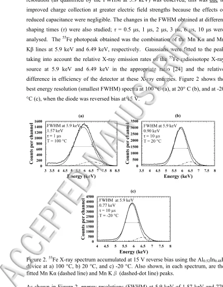
difference in efficiency of the detector at these X-ray energies. Figure 2 shows the
best energy resolution (smallest FWHM) spectra at 100 °C (a), at 20° C (b), and at -20
[image:7.612.59.498.114.679.2]°C (c), when the diode was reversed bias at 15 V.
Figure 2. 55Fe X-ray spectrum accumulated at 15 V reverse bias using the Al0.52In0.48P device at a) 100 °C, b) 20 °C, and c) -20 °C. Also shown, in each spectrum, are the fitted Mn K (dashed line) and Mn K (dashed-dot line) peaks.
As shown in Figure 2, energy resolutions (FWHM) at 5.9 keV of 1.57 keV and 770
eV were obtained at 100° C and at -20 °C, respectively. The FWHM at 5.9 keV at 20
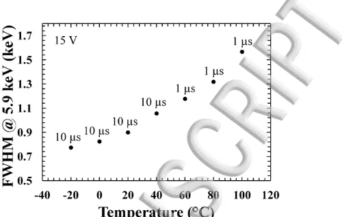
The FWHM was measured for all the spectra accumulated. Figure 3 shows the
FWHM of the 5.9 keV peak as a function of temperature for the shaping time in the
0.5-10 s range at which minimum FWHM was found, when the Al0.52In0.48P device
[image:8.612.205.455.161.320.2]was reversed bias at 15 V.
Figure. 3 FWHM of the5.9 keV peak as a function of temperature at the optimum shaping time and at 15 V.
An increased FWHM was observed at increased temperatures; this was in part
attributed to the higher contribution of the parallel white noise of the system as the
temperature increased.
Three different classes of noise degrade the energy resolution (FWHM) of
non-avalanche X-ray photodiode spectrometers. These are the Fano noise, the charge
trapping noise, and the electronic noise [25]. The statistical nature of the charge
creation process at the absorption of an X-ray determinates the Fano noise; the
expected Fano limited resolution at 5.9 keV for Al0.52In0.48P at room temperature was
calculated to be 145 eV, considering an electron-hole pair creation energy of 5.34 eV
[26] and assuming a Fano factor of 0.12. The FWHM at 5.9 keV experimentally
observed at 20 °C was greater than the Fano limited resolution, this highlighted that
there was a significant contribution from at least one of the other noise sources. The
electronic noise, due to the Al0.52In0.48P photodiode and the preamplifier, consists of
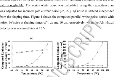
parallel white noise, series white noise, induced gate current noise, 1/f noise and
dielectric noise [25, 27, 28]. The parallel white noise takes into account the leakage
currents of the detector and input JFET of the preamplifier, it is directly proportional
to the shaping time. The series white noise takes into account the capacitances of the
time. The series white noise power spectral density can be approximated to the
thermal noise of the JFET drain current when stray resistance in series with the JFET
gate is negligible. The series white noise was calculated using the capacitance and
was adjusted for induced gate current noise [25, 27]. 1/f noise is instead independent
from the shaping time. Figure 4 shows the computed parallel white noise, series white
noise, 1/f noise at shaping times of 1 s and 10 s, respectively, when the Al0.52In0.48P
[image:9.612.112.497.96.356.2]detector was reversed bias at 15 V.
Figure 4. Computed equivalent noise charge as a function of temperature using the Al0.52In0.48P device at shaping times of a) 1 s and b) 10 s. In both graphs the parallel white noise (empty circles), the series white noise (empty squares) and the 1/f noise (empty triangles) contributions are shown; interpolating lines between the experimental data points (dashed-dot lines) are also shown but must be considered guides for the eye only.
The combined contribution of the dielectric noise and charge trapping noise at 5.9
keV was calculated by subtracting in quadrature the Fano noise, parallel white noise,
series white noise, and 1/f noise contributions at 5.9 keV from the measured FWHM
at 5.9 keV. Figure 5 shows the calculated combined dielectric and trapping noise
contributions at 5.9 keV as a function of temperature, when the Al0.52In0.48P
Figure. 5. Equivalent noise charge of the dielectric and trapping noise contribution at 5.9 keV as a function temperature.
The dielectric and trapping noise contribution at 5.9 keV increased from (70 7) eV to (101 10) eV, when the temperature was increased from -20 °C to 100 °C. At 15
V, the charge trapping noise was negligible as a consequence of improved charge
transport at higher electric fields, in accordance with ref. [1]. Therefore, the increase
in the equivalent noise charge, observed in Figure 5, can be attributed to the dielectric
noise contribution increasing when the temperature was increased. The dependence of
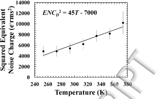
the dielectric equivalent noise charge (ENCD) from the temperature is given by,
ENCD
q A kTDC (1)
where q is the electric charge, A2is a constant (1.18) depending on the type of signal
shaping [27], k is the Boltzmann constant, D is the dissipation factor and C is the
capacitance [25]. A linear least squares fit of the square of the dielectric noise data
showed a linear dependence on the temperature. The gradient determined by the linear
least squares fit was (45 ± 6) [e- rms]2 K-1; an effective dielectric dissipation factor as
high as (7.0 ± 0.9) 10-3
was estimated, but it should be noted that this does not
correspond directly to the dissipation factor of Al0.52In0.48P, rather it is indicative of
the effective combined dissipation factor of all dielectrics contributing to this noise as
it is analyzed here. Figure 6 shows the corresponding linear least squares fit.
Comparison of the standard deviations of the fitting with the experimental
uncertainties demonstrated that linear fitting was appropriate within the limitations of
Figure. 6. Squared equivalent noise charge (ENCD2) of the dielectric noise at 5.9 keV as a function temperature in Kelvin (circles). Also shown is the line of the best fit computed by linear least squares fitting.
The energy resolutions at 5.9 keV for the Al0.52In0.48P photodiode at high temperatures
were worse than the energy resolutions at 5.9 keV observed for SiC and GaAs
detectors at the same temperatures. At 100 °C, a FWHM of 1.57 keV at 5.9 keV was
obtained here, whilst a FWHM of 233 eV at 5.9 keV was reported by Bertuccio et al.
[9] for SiC detectors. The better energy resolution observed by Bertuccio et al. [9]
was attributed to the lower electronic noise associated with their device’ readout
electronics, the thicker detector (lower capacitance) and also the extremely high
quality materials used. At 60 °C, a FWHM of 1.12 keV at 5.9 keV was achieved here,
whilst a FWHM of 840 eV at 5.9 keV was obtained by Lioliou et al. [12] for GaAs
detectors. Since in the presently reported Al0.52In0.48P study device readout electronics
similar to Lioliou et al. [12] was used, the better performance of the GaAs X-ray
spectrometer was in part attributed to the lower electron hole pair creation energy of
GaAs [29] with respect to that one of Al0.52In0.48P. For example, a total noise at the
input of the preamplifier of 86 e- rms corresponds to 840 eV in GaAs, whilst the same
noise equates to a resolution of 1.08 keV in Al0.52In0.48P, due to the difference in
electron-hole pair creation energy. The FWHM observed at 5.9 keV for the
Al0.52In0.48P spectrometer was greater than 1.08 keV suggesting a slightly higher total
noise for the Al0.52In0.48P spectrometer (93 e- rms) with respect to the previously
reported GaAs spectrometer (86 e- rms) [12]. The 93 e- rms total noise in the
Al0.52In0.48P system was calculated by summing in quadrature the 12 e- rms Fano
noise (c.f. 13 e- rms in GaAs [12]), the 58 e- rms parallel white noise (c.f. 43 e- rms in
-rms 1/f noise (c.f. 4.6 e- rms in GaAs [12]) and the 83 e- rms dielectric noise (c.f. 70 e
-rms in GaAs [12]). The energy resolution achieved with the Al0.52In0.48P detector was,
instead, better than that reported by Barnett et al. using Al0.8Ga0.2As detectors [10]. At
90 °C, a FWHM of 2.2 keV at 5.9 keV was obtained by Barnett et al. [10], although
the readout electronics used in Ref. 10 were not of identical design as those used here.
III. CONCLUSION
In this paper, a non-avalanche 200 m diameter Al0.52In0.48P p+-i-n+ mesa X-ray
photodiode was coupled to a custom-made charge-sensitive preamplifier for the
development of a high temperature tolerant X-ray spectrometer. The detector was
illuminated with an 55Fe radioisotope X-ray source The system was characterised over
the temperature range 100 °C to -20 °C. A dark current density ≤0.6 nA/cm2 at 100 °C
was obtained for the Al0.52In0.48P device at 15 V (75 kV/cm). X-ray spectra were
accumulated with the diode reverse biased at 0 V, 5 V, 10 V, and 15 V, as a function
of temperature; the best energy resolution (as quantified by the FWHM at 5.9 keV)
was observed at 15 V. At 100 °C, the best energy resolution was 1.57 keV (FWHM at
5.9 keV) using a shaping time of 1 s; whilst at -20 °C, the best energy resolution was
770 eV using a shaping time of 10 s. System noise analysis was also carried out.
The different noise contributions were computed as a function of temperature. The
main source of noise limiting the energy resolution of the reported system was the
dielectric noise. The dielectric noise contribution was found to increase as the
temperature was increased.
ACKNOWLEDGMENTS
This work was supported by STFC grants ST/M002772/1 and ST/M004635/1
(University of Sussex, A. M. B., PI) and Royal Society Grant RS130515 (University
of Sussex, A. M. B., PI). The authors are grateful to R. J. Airey and S. Kumar at the
EPSRC National Centre for III-V Technologies for device fabrication. G. Lioliou
acknowledges funding received in the form of a PhD scholarship from the University
of Sussex. T. Gohil acknowledges funding received in the form of a PhD studentship
from the Engineering and Physical Sciences Research Council, UK, and the
University of Sussex, UK.
1
S. Butera, G. Lioliou, A. B. Krysa, and A. M. Barnett, J. Appl. Phys. 120, 024502 (2016).
2A. Auckloo, J. S. Cheong, X. Meng, C. H. Tan, J. S Ng, A. B Krysa, R. C. Tozer,
and J. P. R. David, J. Inst.11, P03021 (2016).
3
J. S. Cheong, J. S. Ong, J. S Ng, A. B Krysa, and J. P. R. David, IEEE J. Sel. Topics Quantum Electron. 20, 142 (2014).
4
J. S. L. Ong, J. S. Ng, A. B. Krysa, and J. P. R. David, IEEE Electron Device Letters 32, 1528 (2011).
5
L.Qiao, J. S. Cheong, J. S. Ong, J. S Ng, A. B Krysa, A. B. Green and J. P. R. David, IEEE Photon. Technol. Lett. 28, 481 (2016).
6
D. T. Cromer, and D. Liberman, J. Chem. Phys 53, 1891 (1970).
7
R. Jenkins, R. W. Gould, and D. Gedcke, Quantitative X-ray Spectrometry, Second Ed. (CRC Press, New York, 1995).
8 U. V. Desnica, Prog. Cryst. Growth Charact. Mater. 36, 291 (1998).
9G. Bertuccio, S. Caccia, D. Puglisi, and D. Macera, Nucl. Instrum. Meth. Phys. Res.,
Sect. A 652, 193 (2011).
10
A. M. Barnett, D. J. Bassford, J. E. Lees, J. S. Ng, C. H. Tan, and J. P. R. David, Nucl. Instrum. Meth. Phys. Res., Sect. A 621, 453 (2010).
11
A. M. Barnett, J. E. Lees, D. J. Bassford, J. S. Ng, C. H. Tan, N. Babazadeh, and R. B. Gomes, Nucl. Instrum. Meth. Phys. Res., Sect. A 654, 336 (2011).
12
G. Lioliou, X. Meng, J. S. Ng, and A. M. Barnett, J. Appl. Phys. 119, 124507 (2016).
13
A. Owens, Compound semiconductor radiation detectors, (CRC Press, Boca Raton, 2012).
14M. R. Squillante and G. Entine Nucl. Instrum. Meth. Phys. Res. A 380, 160 (1996).
15S. U. Egarievwe, K. T. Chen, A. Burger, R. B. James, and C.M. Lisse, J. X-ray Sci.
Technol. 6, 309 (1996).
16
P. J. Sellin, Nucl. Instr. and Meth. A 563, 1 (2006).
17
18
L. Abbene, G. Gerardi, and F. Principato, Nucl. Instrum. Meth. Phys. Res. A 777, 54 (2015).
19
M. Prokesch, S. A. Soldner, A. G. Sundaram, M. D. Reed, H. Li, J. F. Eger, J. L. Reiber, C. L. Shanor, C. L. Wray. A. J. Emerick, A. F. Peters, and C. L. Jones, IEEE Trans. Nucl. Sci. 63, 1854 (2016).
20
L. Abbene, G. Gerardi, A. A. Turturici, G. Raso, G. Benassi, M. Bettelli, N. Zambelli, A. Zappettini, and F. Principato, Nucl. Instrum. Meth. Phys. Res. A 835, 1 (2016).
21
A. Zappettini, D. Macera, G. Benassi, N. Zambelli, D. Calestani, M. Ahangarianabhari, Y. Shi, G. Rotondo, B. Garavelli, P. Pozzi, and G. Bertuccio, IEEE Nuclear Science Symposium and Medical Imaging Conference (NSS/MIC), (2014).
22
Keithley Instruments, Inc, Model 6487 Multi-Frequency LCR Meter Manual, 6487-901-01 Rev B, (Cleveland, 2011).
23
Bertuccio, P. Rehak, and D. Xi, Nucl. Instrum. Meth. Phys. Res. B 326, 71 (1993).
24
U. Shotzig, Applied Radiation and Isotopes 53, 469 (2000).
25
G. Lioliou, and A. M. Barnett, Nucl. Instrum. Meth. Phys. Res. A 801, 63 (2015).
26
S. Butera, G. Lioliou, A. B. Krysa, and A. M. Barnett, Electron-hole pair creation energy in Al0.52In0.48P, submitted to Sci. Rep. (2016).
27
G. A. Bertuccio, A. Pullia, and G. De Geronimo, Nucl. Instrum. Meth. Phys. Res. A 380, 301 (1996).
28
E. Gatti, P. F. Manfredi, M. Sampietro, and V. Speziali, Nucl. Instrum. Meth. Phys. Res., A 297, 467 (1990).
29