Persistent template effect in InAs/GaAs quantum dot bilayers
E. Clarke,1,a兲 P. Howe,1 M. Taylor,1 P. Spencer,1 E. Harbord,1 R. Murray,1 S. Kadkhodazadeh,2D. W. McComb,2B. J. Stevens,3and R. A. Hogg3 1
Department of Physics, Blackett Laboratory, Imperial College London, Prince Consort Road, London SW7 2AZ, United Kingdom
2Department of Materials, Imperial College London, Exhibition Road, London SW7 2AZ, United Kingdom 3School of Electronic and Electrical Engineering, University of Sheffield, Sheffield S1 3JD,
United Kingdom
共Received 2 November 2009; accepted 21 April 2010; published online 1 June 2010兲
The dependence of the optical properties of InAs/GaAs quantum dot共QD兲 bilayers on seed layer growth temperature and second layer InAs coverage is investigated. As the seed layer growth temperature is increased, a low density of large QDs is obtained. This results in a concomitant increase in dot size in the second layer, which extends their emission wavelength, reaching a saturation value of around 1400 nm at room temperature for GaAs-capped bilayers. Capping the second dot layer with InGaAs results in a further extension of the emission wavelength, to 1515 nm at room temperature with a narrow linewidth of 22 meV. Addition of more InAs to high density bilayers does not result in a significant extension of emission wavelength as most additional material migrates to coalesced InAs islands but, in contrast to single layers, a substantial population of regular QDs remains. ©2010 American Institute of Physics.关doi:10.1063/1.3429226兴
I. INTRODUCTION
There has been much interest in the growth of closely stacked quantum dot共QD兲layers, for example, to optimize the design of device structures to maximize optical gain,1,2to extend their emission wavelength,3,4 and also to develop novel applications, such as potential qubits for quantum in-formation processing.5,6 When there is a sufficiently small separation between two QD layers, strain from the underly-ing layer influences the growth conditions of an upper layer, leading to preferential nucleation of QDs above buried QDs.7 This provides an additional control mechanism over the growth process and allows greater freedom of choice of QD properties in stacked QD layers than is possible for single layers. Typical growth parameters such as coverage,3 temperature,4and growth rate8can be varied to tune the size and composition of QDs in the upper layer while keeping the QD density constant, since the lower 共seed兲 layer acts as a template for QD nucleation. These InAs/GaAs QD bilayers have been successfully incorporated into edge-emitting laser structures with room temperature operation at wavelengths up to 1430 nm.8
In this paper we examine two aspects of the growth of InAs/GaAs QD bilayers. In the first part of the paper we investigate the effect of the seed layer growth conditions on the structural and optical properties of QD bilayers, with the aim of extending the QD emission wavelength. Techniques for growth of InAs/GaAs QDs with room temperature emis-sion at 1300 nm are now well established,9–11 but further extension of InAs/GaAs QD emission wavelength toward the 1550 nm telecoms window is rarely reported.12–16 By varia-tion in the growth temperature of the seed layer, the number density of seed QDs can be varied over a range of 40– 300 m−2in a simple and reproducible manner. This in
turn results in a comparable change in QD density in the second layer of bilayer structures and an accompanying variation in the height of QDs. The larger QD size allows extension of the room temperature emission of the InAs/ GaAs QD bilayers from 1340 nm to around 1400 nm using GaAs capping. This range can be extended beyond 1500 nm when the second layer is InGaAs capped.
In the second part, we investigate increasing the InAs coverage in the second layer of high density QD bilayers. Since the extension of the emission wavelength of the QD bilayers we report in the first part of the paper is achieved by increasing the size of the second layer QDs, it is natural to assume that increasing the InAs coverage in the second layer of the high density bilayers may also result in a similar ex-tension of their emission wavelength. However, previous studies of single QD layers show there is an optimum InAs coverage beyond which saturation in the emission wave-length occurs17 and, as the coverage is increased, large ir-regular islands form, in addition to the stable ensemble of coherent islands.18–20 Increasing the InAs coverage in the second layer of the bilayers does not result in a significant extension of the emission wavelength as the majority of the additional material accumulates in the large islands and the size of the regular, emissive QDs remains approximately constant. However, even at very high InAs coverage 共9 monolayers共ML兲兲, where the structure is dominated by ap-parently coalesced InAs islands, regular-sized InAs islands remain and there is surprisingly little degradation in the room temperature photoluminescence共PL兲intensity obtained from these samples.
II. EXPERIMENTAL DETAILS
Samples were grown by molecular beam epitaxy on un-doped GaAs共001兲 substrates. Following oxide removal and growth of a 200 nm GaAs buffer, the GaAs surface was
a兲Electronic mail: [email protected].
annealed at a substrate temperature of 580 ° C under an As2
flux for 10 min. The temperature was then reduced for growth of the seed QD layer by deposition of 2.4 ML InAs. An InAs growth rate of 0.014 ML s−1 was used for all the
samples. The first study investigates the dependence of dot density on growth temperature of the seed layer in the range 475 to 515 ° C 共the lower and upper ends of this range are dictated by the quality of the GaAs capping layer and In desorption, respectively兲. Uncapped seed layer samples were used for atomic force microscopy 共AFM兲 characterization, while completed structures were grown using the following recipe: the seed layer was capped by a 10 nm GaAs spacer layer grown at the same temperature and the sample was again annealed for 10 min at 580 ° C in order to smooth the GaAs surface and desorb any segregated In.21 The tempera-ture was then reduced to 467 ° C for growth of 3.3 ML InAs to form the second QD layer; this eliminates In/Ga intermixing.4For the second study the seed layer was grown at a temperature of 475 ° C while the amount of InAs used to form the second layer covered the range 3.7–9.0 ML.
Samples for AFM characterization of the second layer were left uncapped but samples for PL were capped, either by 100 nm GaAs or by a 4 nm In0.26Ga0.74As layer followed by the remaining共96 nm兲GaAs cap. The first 15 nm of the capping layers was grown at 467 ° C before the temperature was increased to the optimum GaAs growth temperature of 580 ° C. AFM measurements were performed using a Digital Instruments atomic force microscope in contact mode for the initial seed layer growth temperature study and tapping mode for the second layer InAs coverage study. Samples for trans-mission electron microscopy 共TEM兲 characterization were prepared by mechanical polishing followed by Ar ion milling and images were obtained using JEOL 2010 TEM operating at 200 kV. PL spectra were obtained using a HeNe laser, dispersing the emitted light with a SPEX 0.5 m monochro-mator, with detection by a cooled Ge diode using standard lock-in techniques.
III. RESULTS AND DISCUSSION
A. Effect of seed layer growth temperature
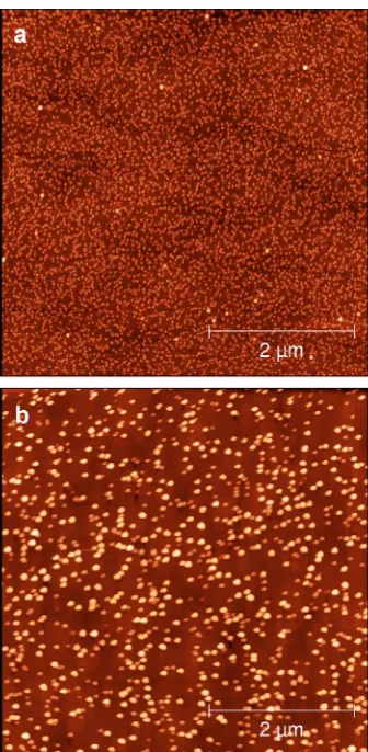
The AFM images shown in Fig.1illustrate the variation in the size and density of QDs that can be obtained by chang-ing the growth temperature from 480 to 515 ° C. At 480 ° C, a relatively high density of 3.1⫻1010 cm−2of small islands
共with an average island height of 6.1 nm and base diameter of 57 nm兲is formed, despite the low InAs growth rate used. At 515 ° C, a sixfold lower island density is obtained, with a corresponding increase in the size of the InAs islands to an average height of 15.1 nm and base diameter of 100 nm. This is not surprising since the same amount of deposited In is now distributed among fewer islands and the higher growth temperature is likely to lead to increased Ga inclusion from the substrate.22A similar change in the seed layer density can also be achieved by varying the InAs growth rate;23however, we have chosen to vary the growth temperature in order to maintain a constant In cell temperature 共and InAs growth rate兲for growth of both QD layers.
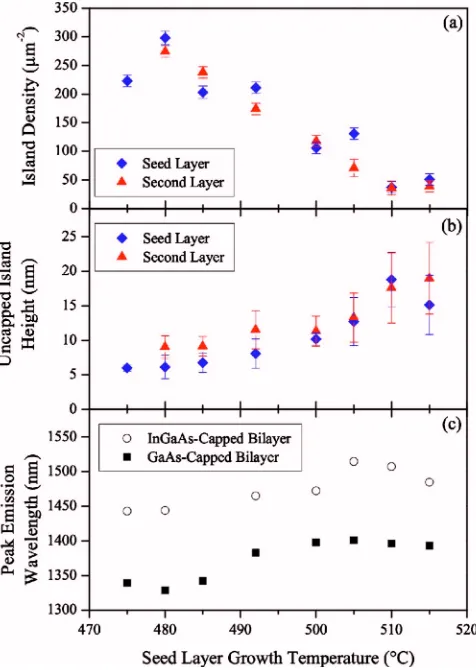
Figure2共a兲summarizes an analysis of AFM images ob-tained from uncapped seed layers and bilayers. It shows a monotonic reduction in island density in both layers as the seed layer growth temperature is increased. Both layers fol-low the same trend, with approximately equal densities in both layers over the whole temperature range, indicating that the seed layer acts as a highly effective template for the growth of the second layer QDs and that the majority of QDs in the bilayers must be vertically correlated.7As the island density decreases there is a concomitant increase in the av-erage height of islands in both layers, as shown in Fig.2共b兲. It is well known that when islands are capped, they rapidly collapse in height but larger islands are expected to better maintain their height and have a larger In-content once capped.24The inset to Fig.3shows a bright field TEM image obtained from a bilayer sample with a seed layer grown at 492 ° C. There is a clear vertical correlation between the QDs in the bilayer, and we can estimate a height of⬃5 nm for the seed layer QDs and 7–8 nm for QDs in the second layer. These are likely to be overestimates since contrast in the TEM images will include both compositional and strain components but these values are certainly smaller than those deduced from AFM samples 关8.1 nm 共seed layer兲 and 11.5 nm 共second layer兲兴 grown under the same conditions 关Fig. 2共b兲兴.
[image:2.612.352.520.46.389.2]With an increase in the size of capped QDs, one would expect an increase in the emission wavelength, especially FIG. 1. 共Color online兲5⫻5 m2AFM images obtained from uncapped
since the low growth temperature for the second layer
[image:3.612.54.292.49.384.2]共467 ° C for all samples兲 will suppress In/Ga intermixing. Figure2共c兲shows that the peak room temperature PL emis-sion obtained from the GaAs-capped bilayer samples in-creases from 1340 nm up to a saturation value of around 1400 nm with increasing growth temperature of the seed layer. For single layers, such saturation in emission wave-length is due to saturation in QD size17 but the AFM data presented in Fig.2共b兲indicates that this is not the case here. We speculate that the saturation in wavelength may occur despite the increase in the size of the QDs if the increased size of the seed layer QDs modifies the strain field experi-enced by the second layer QDs, leading to increased In/Ga intermixing or strain-related modification of the energy lev-els in these QDs. Alternatively, the second layer QDs may reach a threshold in size beyond which dislocation occurs, placing a limit on the maximum size of the emissive QDs. The maximum peak wavelength is comparable with the long-est reported emission wavelengths for GaAs-capped InAs/ GaAs QDs.25,26However in these previous studies, the QDs were grown at extremely low rates, resulting in an areal den-sity an order of magnitude lower than for the bilayers dis-cussed here. The emission wavelength of these bilayers is still longer than that reported for many InGaAs-capped or dots-in-a-well structures and yet the bilayers do not contain InGaAs strain-reducing layers. When such layers are incor-porated, by initially capping the second layer QDs with 4 nm In0.26Ga0.74As, the peak emission of the bilayers is further extended by⬃100 nm. Figure3shows a room temperature PL spectrum obtained from an InGaAs-capped bilayer QD sample where the seed layer was grown at 505 ° C. The peak emission for this sample occurs at 1515 nm, which is the longest wavelength reported for a QD bilayer and is compa-rable with the longest wavelengths obtained from any QDs grown on GaAs substrates.12–16 The emission has a narrow PL linewidth of 22 meV, which is consistent with previous reports of narrow emission linewidths from InAs/GaAs bilayers4,27 and indicates a high degree of uniformity of the QDs. Emission from the seed layer is suppressed due to ef-ficient electronic coupling between the layers: room tempera-ture emission from the seed layer is expected to be around 1250 nm for QDs grown under these conditions. The sup-pression of seed layer emission also persists to low tempera-tures共not shown兲. From the TEM image inset to Fig.3, we note that although the spacer layer between the two QD lay-ers is 10 nm GaAs, the actual barrier thickness between a pair of vertically correlated QDs is around 5 nm. Previous studies have also demonstrated efficient electronic coupling between QD layers separated by a GaAs spacer layer of 10 nm共Refs.2and28兲and an excitation transfer time of 20 ps has been estimated for bilayer QDs with a similar separation, which is short compared to ground state共GS兲radiative life-time of the seed layer QDs.29Further extension of the emis-sion wavelength may be possible by optimization of the In-GaAs cap30but our initial studies indicate that capping with a higher In-content or thicker InGaAs cap results in a signifi-cant deterioration in PL intensity.
FIG. 2. 共Color online兲 共a兲Variation in QD density in the seed layer共 dia-monds兲and the second layer of InAs/GaAs QD bilayers共triangles兲with change in the seed layer growth temperature. Note that the growth tempera-ture of the second layer remains the same共467 ° C兲for all bilayer samples. 共b兲Variation in average QD height in the seed layer共diamonds兲and the second layer of InAs/GaAs QD bilayers共triangles兲with change in the seed layer growth temperature. The larger error bars for the lower density samples共high seed layer temperature兲are due to the smaller number of QDs analyzed.共c兲Variation in peak room temperature emission from InAs/GaAs QD bilayers capped either by GaAs共closed squares兲or additionally by an InGaAs strain-reducing layer共open circles兲with change in the seed layer growth temperature.
FIG. 3. Room temperature PL spectrum obtained from an InAs/GaAs QD bilayer with the seed layer grown at 505 ° C and the second layer capped by 4 nm In0.26Ga0.74As. Noise around 1350–1400 nm is due to water
[image:3.612.68.276.542.708.2]B. Increasing InAs coverage in the second layer
Achieving room temperature emission from InAs/GaAs QDs beyond 1500 nm without recourse to InGaAs metamor-phic buffer layers14 or complex quaternary strain-reducing layers such as InGaNAs共Ref.15兲or InGaAsSb共Ref.16兲is of interest for device applications, although for many of these applications an increased QD density is also desirable. One would expect that the size of QDs in high density samples could be increased by depositing additional mate-rial. However, for single layer growth there is saturation in both QD size and emission wavelength as InAs coverage is increased17 and alongside the stable ensemble of coherent islands, a small number of large, irregular InAs islands form. These large islands rapidly grow in size as more material is deposited. Frigeri et al.18 have observed the onset of these irregular islands in single layer InAs/GaAs QD growth after 2.4 ML InAs deposition, with the density of these islands rising from 2 m−2for 2.4 ML InAs to 15 m−2for 2.9 ML InAs coverage. A low density 共1.2 m−2兲 of large islands can be seen in the AFM image of the seed layer grown at 480 ° C 关Fig.1共a兲兴. The appearance of increased numbers of these large islands also coincides with the InAs coverage required for significant defect formation in InAs/GaAs QD layers,19and an accompanying decrease in PL intensity from capped samples.18As the InAs coverage is further increased, the irregular islands act as a strain-free sink for surface ada-toms during growth, and material migrates away from nor-mal, coherent islands and accumulates almost exclusively in the large islands.20 The bilayers discussed in Sec. III A are grown using a higher InAs coverage in the second layer共3.3 ML兲than is typical for single QD layers but despite this the
density of large, irregular islands in the second layer of the bilayers remains an order of magnitude lower than reported for single layers,18around 1 – 2 m−2. We tentatively ascribe this to strain relief provided by the seed layer which inhibits the onset of irregular islands,31 although the formation of these islands may also be dependent on the As overpressure during growth.
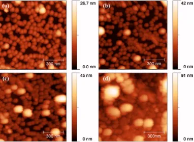
To investigate the effect of increased InAs coverage in the second layer of the bilayers, samples were grown using a high density seed layer共grown under the same conditions as outlined earlier, with a seed layer growth temperature of 475 ° C兲and with an InAs coverage in the second layer rang-ing from 3.7–9.0 ML. Figure4 shows 1⫻1 m2AFM
[image:4.612.117.499.49.328.2]im-ages obtained from a selection of these samples. Figure4共a兲 is from the sample grown with 3.7 ML InAs coverage in the second layer: the majority of the islands are of a similar size and shape, with only a few islands significantly taller than the others, although the number of these large islands is in-creased from that seen for samples with 3.3 ML InAs cover-age. The average height of the regular islands is 8.5 nm, which is comparable with the average island height for rea-sonably high density bilayers presented in Fig.2共b兲. As more InAs is deposited the proportion of regular-sized islands di-minishes while the number and size of large, irregular islands increases, at least up to 9.0 ML, the largest InAs coverage used in this series of samples. At this InAs coverage, shown in Fig.4共d兲, the majority of the deposited material has accu-mulated in the irregular islands and accounts for roughly half of the sample surface, although some normal-sized islands remain. This is in contrast to previous reports for single layer QD growth, where coverage beyond⬃4 ML results only in FIG. 4.共Color online兲Plan view 1⫻1 m2AFM images obtained from InAs/GaAs QD bilayers with seed layer grown at 475 ° C and InAs coverage in the
large, irregular islands.20 We conclude that the underlying seed layer provides robust island nucleation sites that can retain adatoms despite the presence of nearby dislocated is-lands. Previous theoretical analysis of strain in bilayers sug-gests that underlying QDs can have a significant influence on In diffusion during second layer growth: for the GaAs spacer thickness used here, the In diffusion coefficient is reduced to less than 80% above a buried QD compared with its value for an unstrainedc共4⫻4兲GaAs surface.32
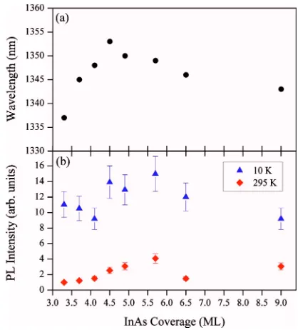
Figure 5共a兲 summarizes the AFM data and shows the density of both the normal and the large, coalesced islands in the second layer of the bilayers as the InAs coverage is in-creased. The density of normal islands decreases as the num-ber of coalesced islands increases and account for most of the surface area. Figure5共b兲shows the island height for the two populations as the InAs coverage is increased. Although the size of the coalesced islands increases as more material is added, the height of the regular islands remains roughly con-stant at less than 10 nm. This is further illustrated by PL obtained from capped samples. Figure 6共a兲 shows that the room temperature peak emission wavelength of the GS from all samples is around 1350 nm and does not increase as the InAs coverage in the second layer is increased, which is consistent with the constant size of the regular islands in the AFM samples. Surprisingly, the room temperature PL ob-tained from all samples is of a comparable intensity to con-ventional共seed layer only兲QD samples, even for 9 ML InAs coverage, in marked contrast to single layers where
disloca-tion formadisloca-tion leads to a rapid reducdisloca-tion in PL intensity for InAs coverage above 3 ML InAs.18 Figure 6共b兲 shows the peak GS PL intensity obtained from GaAs-capped samples at both low temperature共10 K兲and room temperature共295 K兲. The PL intensity at low temperature is approximately con-stant for all samples while at room temperature the PL inten-sity is reduced by about a factor of 10 from the low tempera-ture value. A reduction in PL intensity due to the reduction in density of regular QDs with increasing InAs coverage which is seen in the AFM analysis关Fig.5共a兲兴is not resolved in our PL measurements, with the variation in PL intensity within that expected for sample-to-sample variations. A similar variation in PL intensity was also observed from nominally identical GaAs/AlGaAs multiple quantum well samples grown for calibration purposes over the same period as these QD samples. We speculate that the reasonably high PL in-tensity obtained from all samples may be a consequence of efficient carrier capture and transfer from the seed layer to coherent QDs in the second layer providing a source of car-riers for radiative recombination.
IV. SUMMARY
[image:5.612.69.275.46.362.2]We have investigated two aspects of InAs/GaAs QD bi-layer growth conditions and their influence on QD size, with the intention of obtaining larger QDs with long emission wavelengths. This can effectively be achieved by varying the growth conditions for the seed layer, thereby altering the template for second layer growth. Efficient strain coupling ensures that a change in seed layer QD density results in a similar change in the QD density in the upper layer of bilayer structures, and as the QD density is reduced the QDs in the upper layer are increased in size, leading to an increase in the peak emission wavelength to a maximum value of 1400 nm at room temperature for GaAs-capped bilayers and 1515 nm for InGaAs capped layers. However, depositing more InAs to FIG. 5. 共Color online兲 共a兲Density and 共b兲height of regular-sized islands
[image:5.612.330.539.47.278.2]共triangles兲and large, coalesced islands共diamonds兲in the second layer of QD bilayer as InAs coverage is increased from 3.7 to 9.0 ML.
the second layer of high density QD bilayers does not sig-nificantly extend the emission wavelength as the extra mate-rial accumulates in coalesced islands but the presence of the seed layer maintains a population of regular, emissive QDs, providing room temperature luminescence even for ex-tremely high InAs coverage in the second layer.
1A. E. Zhukov, A. R. Kovsh, N. A. Maleev, S. S. Mikhrin, V. M. Ustinov,
A. F. Tsatsul’nikov, M. V. Maximov, B. V. Volovik, D. A. Bedarev, Y. M. Shernyakov, P. S. Kop’ev, Z. I. Alferov, N. N. Ledentsov, and D. Bim-berg,Appl. Phys. Lett.75, 1926共1999兲.
2E. C. Le Ru, A. J. Bennett, C. Roberts, and R. Murray,J. Appl. Phys.91,
1365共2002兲.
3I. Mukhametzhanov, R. Heitz, J. Zeng, P. Chen, and A. Madhukar,Appl.
Phys. Lett.73, 1841共1998兲.
4E. C. Le Ru, P. Howe, T. S. Jones, and R. Murray,Phys. Rev. B67,
165303共2003兲.
5G. Burkard, G. Seelig, and D. Loss,Phys. Rev. B62, 2581共2000兲. 6M. Bayer, P. Hawrylak, K. Hinzer, S. Fafard, M. Korkusinski, Z. R.
Wasilewski, O. Stern, and A. Forchel,Science291, 451共2001兲.
7Q. Xie, A. Madhukar, P. Chen, and N. P. Kobayashi,Phys. Rev. Lett.75,
2542共1995兲.
8L. H. Li, M. Rossetti, A. Fiore, and G. Patriarche,Electron. Lett.42, 638
共2006兲.
9R. Murray, D. Childs, S. Malik, P. Siverns, C. Roberts, J.-M. Hartmann,
and P. Stavrinou,Jpn. J. Appl. Phys., Part 138, 528共1999兲.
10K. Nishi, H. Saito, S. Sugou, and J.-S. Lee,Appl. Phys. Lett.74, 1111
共1999兲.
11V. M. Ustinov, N. A. Maleev, A. E. Zhukov, A. R. Kovsh, A. Y. Egorov,
A. V. Lunev, B. V. Volovik, I. L. Krestnikov, Y. O. Musikhin, N. A. Bert, P. S. Kop’ev, Z. I. Alferov, N. N. Ledentsov, and D. Bimberg,Appl. Phys. Lett.74, 2815共1999兲.
12J. Tatebayashi, M. Nishioka, and Y. Arakawa,Appl. Phys. Lett.78, 3469
共2001兲.
13T.-P. Hsieh, P.-C. Chiu, J.-I. Chyi, N.-T. Yeh, W.-J. Ho, W.-H. Chang, and
T.-M. Hsu,Appl. Phys. Lett.87, 151903共2005兲.
14N. N. Ledentsov, A. R. Kovsh, A. E. Zhukov, N. A. Maleev, S. S.
Mikhrin, A. P. Vasil’ev, E. S. Semenova, M. V. Maximov, Y. M. Shernya-kov, N. V. Kryzhanovskaya, V. M. Ustinov, and D. Bimberg,Electron. Lett.39, 1126共2003兲.
15M. Richter, B. Damilano, J.-Y. Duboz, J. Massies, and A. D. Wieck,Appl.
Phys. Lett.88, 231902共2006兲.
16D. Guimard, S. Tsukamoto, M. Nishioka, and Y. Arakawa,Appl. Phys.
Lett.89, 083116共2006兲.
17P. B. Joyce, T. J. Krzyzewski, G. R. Bell, T. S. Jones, E. C. Le Ru, and R.
Murray,Phys. Rev. B64, 235317共2001兲.
18P. Frigeri, L. Nasi, M. Prezioso, L. Seravalli, G. Trevisi, E. Gombia, R.
Mosca, F. Germini, C. Bocchi, and S. Franchi,J. Appl. Phys.102, 083506 共2007兲.
19J. S. Wang, J. F. Chen, J. L. Huang, P. Y. Wang, and X. J. Guo,Appl. Phys.
Lett.77, 3027共2000兲.
20D. Leonard, K. Pond, and P. M. Petroff,Phys. Rev. B50, 11687共1994兲. 21P. Howe, E. C. Le Ru, E. Clarke, R. Murray, and T. S. Jones, J. Appl.
Phys.98, 113511共2005兲.
22P. B. Joyce, T. J. Krzyzewski, G. R. Bell, B. A. Joyce, and T. S. Jones,
Phys. Rev. B58, R15981共1998兲.
23P. B. Joyce, T. J. Krzyzewski, G. R. Bell, T. S. Jones, S. Malik, D. Childs,
and R. Murray,Phys. Rev. B62, 10891共2000兲.
24P. B. Joyce, T. J. Krzyzewski, G. R. Bell, and T. S. Jones,Appl. Phys. Lett.
79, 3615共2001兲.
25B. Alloing, C. Zinoni, V. Zwiller, L. H. Li, C. Monat, M. Gobet, G. Buchs,
A. Fiore, E. Pelucchi, and E. Kapon,Appl. Phys. Lett.86, 101908共2005兲.
26D. Guimard, H. Lee, M. Nishioka, and Y. Arakawa,Appl. Phys. Lett.92,
163101共2008兲.
27Z. Mi and P. Bhattacharya,J. Appl. Phys.98, 023510共2005兲.
28P. Howe, E. C. Le Ru, E. Clarke, B. Abbey, R. Murray, and T. S. Jones,J.
Appl. Phys.95, 2998共2004兲.
29R. Heitz, I. Mukhametzhanov, P. Chen, and A. Madhukar,Phys. Rev. B
58, R10151共1998兲.
30L. Seravalli, M. Minelli, P. Frigeri, S. Franchi, G. Guizzetti, M. Patrini, T.
Ciabattoni, and M. Geddo,J. Appl. Phys.101, 024313共2007兲.
31I. Daruka and A.-L. Barabási,Phys. Rev. Lett.79, 3708共1997兲. 32S. Tomić, P. Howe, N. M. Harrison, and T. S. Jones,J. Appl. Phys.99,