FAKULTI KEJURUTERAAN ELEKTRIK
UNIVERSITI TEKNIKAL MALAYSIA MELAKA
LAPORAN PROJEK
SARJANA MUDA
DESIGN AND SIMULATION OF DC-DC SWITCHING BOOST CONVERTER FOR CURRENT RIPPLE REDUCTION
Nur Ani binti Nasrudin
Bachelor of Electrical Engineering
“I hereby declare that I have read through this report entitle “Design and Simulation of a
DC-DC Switching Boost Converter For Current Ripple Reduction” and found that it has comply
the partial fulfillment for awarding the degree of Bachelor of Electrical Engineering (Industrial
Power)”
Signature : ...
Supervisor‟s Name : ...
DESIGN AND SIMULATION OF DC-DC SWITCHING BOOST CONVERTER FOR
CURRENT RIPPLE REDUCTION
NUR ANI BINTI NASRUDIN
A report submitted in partial fulfilment of the requirements for the degree of Electrical
Engineering (Industrial Power)
Faculty of Electrical Engineering
UNIVERSITI TEKNIKAL MALAYSIA MELAKA
I declare that this report entitle “Design and Simulation of a DC-DC Switching Boost
Converter for Current Ripple Reduction” is the result of my own research except as cited in
the references. The report has not been accepted for any degree and is not concurrently
submitted in candidature of any other degree.
Signature : ...
Name : ...
To my beloved family,
Abah Mama Along
ACKNOWLEDGEMENT
First and foremost, I would like to express my greatest gratitude to god the Almighty
without his blessings I would never be able to complete this Final Year Project.
I would like to thank University Teknikal Malaysia Melaka for providing me a path to
further my studies. The excellent facilities are truly appreciated. Not to forget, this final year
project would not have been possible without my supervisor, Ir. Dr. Rosli bin Omar, who has
supported me throughout my project with his patience and knowledge while allowing me the
room to work in my own way. Without his encouragement this project would not have been
completed. One simply could not wish for a better or friendlier supervisor.
In the laboratory, I am grateful to have been aided by En. Anggun, who has helped me
throughout the completion of the project whenever I am lost or in doubts.
In my daily work, I have been blessed with a friendly and cheerful group of fellow
friends who have provided me with good arguments concerning about theoretical and
experimental matters which helped me regain some sort of fitness of a healthy body and a
healthy mind.
Last but not least, I would like to thank my parents and siblings for their love,
ABSTRACT
This project is to simulate and to design a DC-DC switching boost converter for current ripple
reduction. Step up converter is also referred to boost converter where its characteristic is to
have a voltage at the output that is larger than the voltage at the input. The converter operates
by opening and closing an electronic switch such as a power MOSFET, IGBT’s or thyristors
periodically. Ripple exist during the switching process in the DC-DC converter where the
change or switching from the ON state and OFF state produces current ripple in the inductor.
By reducing the current ripple in the DC-DC switching boost converter, the efficiency of the
DC-DC switching boost converter will increase. Methods that is available for current ripple
reduction includes by increasing the value of the inductor, by using soft-switching techniques
and also by the adaptation of interleaving technologies. The method of varying the value of
inductance to reduce the current ripple in the DC-DC boost converter is presented in this
paper.
ABSTRAK
Projek ini adalah bertujuan untuk mensimulasi dan mereka bentuk satu arus terus
peningkatan pensuisian arus terus penukar untuk pengurangan riak arus. Meningkatkan
penukar juga dirujuk kepada peningkatan penukar di mana biasanya mempunyai nilai
voltan di output yang lebih besar daripada nilai voltan di input. Penukar beroperasi
dengan kondisi di mana suis elektronik di buka dan di tutup secara berkala oleh suis
elektronik sperti MOSFET, IGBT atau thyristor. Gelombang atau riak ini wujud dalam
proses pensuisan dalam arus terus penukar di mana perubahan dari kondisi buka kepada
kondisi tutup menghasilkan riak dalam pengaruh. Dengan mengurangkan riak arus
dalam arus terus peningkatan pensuisan arus terus penukar, kecekacan arus terus
peningkatan pensuisan arus terus penukar dapat ditingkatkan. Cara yang tersedia ada
untuk mengurangkan riak arus terus termasuklah dengan menambahkan nilai pengarun,
dengan menggunakan teknik penukar lembut dan juga oleh penyesuaian pengantara
lembaran teknologi. Kaedah mempelbagaikan nilai aruhan untuk mengurangkan riak
arus dalam arus terus peningkatan arus terus ini akan dibentangkan di dalam kertas tulis
ini.
TABLE OF CONTENT
CHAPTER
TITLE
PAGE
ABSTRAK i
ABSTRACT ii
DEDICATION iii
ACKNOWLEDGEMENT iv
TABLE OF CONTENT v
LIST OF TABLES vii
LIST OF FIGURES viii
LIST ABBREVIATIONS ix
LIST OF APPENDICES
1 INTRODUCTION
1.1 Background 1
1.2 Problem Statement 2
1.3 Objectives 2
1.4 Scope of Project 3
1.5 Chapter Summary 3
2 LITERATURE REVIEW
2.1 Chapter Introduction 4
2.2 Common Method for Current Ripple Reduction 4
2.2.1 By increasing the value of the inductance 4
2.2.2 Frequency control 5
2.3 Overview of boost converter 6
2.4 Boost Converter Topology 7
2.5 Insulated-Gate Bipolar Transistor (IGBT) 11
2.6 MATLAB Simulink 12
2.7 DSP TMS320F2812 13
2.8 Chapter Summary 13
3 METHODOLOGY
3.1 Introduction 14
3.2 Project Flow Chart 15
3.3 MATLAB Simulink 16
3.4 Code Composer Studio DSP TMS320F2812 18
3.4.1 Flow chart using Code Composer Studio
(CCS) 19
3.5 Program testing 20
3.6 Schematic Design Using Proteus 8 Professional 20
3.7 PCB Etching 22
3.8 Hardware testing 26
3.9 Chapter Summary 26
4 RESULTS
4.1 Introduction 27
4.2 Calculation Results 28
4.2.1 Case 1: The effect towards current ripple
when the value of frequency is varied 29
4.2.2 Case 2: The effect towards current ripple
when the value of duty cycle is varied 31
4.3 Simulation Results 33
4.3.1 Case 1: The effect towards current ripple
when the value of frequency is varied 33
when the value of Duty Cycle Is Varied 40
4.4 Experimental Results 47
4.4.1 Case 1: The effect towards current ripple
when the value of frequency is varies 47
4.4.2 Case 2: The effect towards current ripple
when the value of duty cycle is varied 57
4.5 Chapter Summary 62
5 ANALYSIS AND DISCUSSION
5.1 Chapter introduction 63
5.2 Analysis 63
5.2.1 Analysis on the effect towards the current
ripple when varying the value of frequency 63
5.2.2 Analysis on the effect towards the current
ripple when varying the value of duty cycle 67
5.3 Chapter Summary 70
6 CONCLUSION AND RECOMMENDATION
6.1 Chapter introduction 71
6.2 Conclusion 71
6.3 Recommendation 72
REFERENCES 73
LIST OF TABLES
4.1 Parameters of a boost circuit (frequency is varied) 29
4.2 Current ripple, when the value of frequency is varied 30
4.3 Parameters of a boost circuit (duty cycle is varied) 31
4.4 Current ripple, when the value of duty cycle is varied 32
5.1 ΔiL (A) for calculation, simulation and experimental when varying the
value of frequency 64
LIST OF FIGURES
2.1 Boost converter 6
2.2 Equivalent circuit for switch closed 7
2.3 Equivalent circuit for switch open 8
2.4 Inductor current in continuous current mode 9
2.5 Inductor current discontinuous current mode 10
2.6 IGBT device symbol 11
2.7 Matlab simulink 12
2.8 DSP TMS 320F 2812 13
3.1 Project progress flow chart 15
3.2 Matlab Simulink 16
3.3 Model of a boost circuit 17
3.4 Creating a project 18
3.5 Progress flow chart for Code composer studio (CCS) 19
3.6 Proteus 8 professional 20
3.7 Isis schematic capture 21
3.8 ARES PCB layout 22
3.9 Positive acting PCB 23
3.10 Developing the PCB 23
3.11 Etching the PCB 24
3.12 (a) Drilling process (b) Boost converter box 25
3.13 Hardware testing 26
4.1 DC-DC boost circuit 28
at the inductor 33
4.3 Graph of pulse with a frequency, f of 20 kHz and the current ripple,
at the inductor 34
4.4 Graph of pulse with a frequency, f of 30 kHz and the current ripple,
at the inductor 35
4.5 Graph of pulse with a frequency, f of 40 kHz and the current ripple,
at the inductor 36
4.6 Graph of pulse with a frequency, f of 50 kHz and the current ripple,
at the inductor 36
4.7 Graph of pulse with a frequency, f of 60 kHz and the current ripple,
at the inductor 37
4.8 Graph of pulse with a frequency, f of 70 kHz and the current ripple,
at the inductor 38
4.9 Graph of pulse with a frequency, f of 80 kHz and the current ripple,
at the inductor 39
4.10 Graph of pulse with a duty cycle, D of 10% and the current ripple,
at the inductor 40
4.1 Graph of pulse with a duty cycle, D of 20% and the current ripple,
at the inductor 41
4.12 Graph of pulse with a duty cycle, D of 30% and the current ripple,
at the inductor 41
4.13 Graph of pulse with a duty cycle, D of 40% and the current ripple,
at the inductor 42
4.14 Graph of pulse with a duty cycle, D of 50% and the current ripple,
at the inductor 43
4.15 Graph of pulse with a duty cycle, D of 60% and the current ripple,
at the inductor 44
4.16 Graph of pulse with a duty cycle, D of 70% and the current ripple,
4.17 Graph of pulse with a duty cycle, D of 80% and the current ripple,
at the inductor 45
4.18 Graph of pulse with a duty cycle, D of 90% and the current ripple,
at the inductor 46
4.19 Setup of the boost circuit 47
4.20 Output window 48
4.21 Relationship of T1PR command and T1CMPR command 49
4.22 Current ripple 50
4.23 Pulse with a frequency, f of 10 kHz and the current ripple, iL at the
inductor 51
4.24 Pulse with a frequency, f of 20 kHz and the current ripple, iL at the
inductor 52
4.25 Pulse with a frequency, f of 30 kHz and the current ripple, iL at the
inductor 53
4.26 Pulse with a frequency, f of 40 kHz and the current ripple, iL at the
inductor 54
4.27 Pulse with a frequency, f of 50 kHz and the current ripple, iL at the
inductor 55
4.28 Pulse with a frequency, f of 60 kHz and the current ripple, iL at the
inductor 56
4.29 Pulse with a frequency, f of 70 kHz and the current ripple, iL at the
inductor 56
4.30 Pulse with a duty cycle, D of 10% and the current ripple, iL at the
Inductor 57
4.31 Pulse with a duty cycle, D of 20% and the current ripple, iL at the
Inductor 58
4.32 Pulse with a duty cycle, D of 30% and the current ripple, iL at the
Inductor 58
4.33 Pulse with a duty cycle, D of 40% and the current ripple, iL at the
Inductor 59
Inductor 60
4.35 Pulse with a duty cycle, D of 60% and the current ripple, iL at the
Inductor 60
4.36 Pulse with a duty cycle, D of 70% and the current ripple, iL at the
Inductor 61
4.37 Pulse with a duty cycle, D of 80% and the current ripple, iL at the
Inductor 61
5.1 Obtaining the result from graph 65
5.2 Graph of current ripple reduction by varying the value of frequency 67
5.3 Graph of performance of the current ripple by varying the value of
duty cycle, D 69
LIST OF ABBREVIATIONS
AC - Alternating Current
DC - Direct Current
SEPIC - Single Inductance Converter
IGBT - Insulated Gate Bipolar Transistor
DSP - Digital Signal Processing
MOSFET - Metal Oxide Semiconductor Field Effect Transistor
CCM - Continuous Current Mode
DCM - Discontinuous Current Mode
Lmin - Minimum Inductance
V - Voltage
Vs - Voltage source
D - Duty cycle
f - Frequency
R - Resistance
CCS - Code Composer Studio
LIST OF APPENDICES
PAGES TITLE
A Gantt Chart 76
B Boost converter layout 77
C Boost converter schematic 78
D Input/ output connector and signal description 79
E PWM coding using DSP TMS320F2812 80
F Current transducer LA 100-P 84
G Experimental Setup 85
CHAPTER 1
INTRODUCTION
1.1 Background
As the world evolves to an era where the parameters of a device or component in terms
of size, weight, and performance of technologies are concerned, the power electronic industry
escalates to rise. With the advantage of having a compact system with low losses, high
efficiency, availability, and reliability, new switching circuit topologies, high speed of
response, power electronic operates with digital or analog electronic control circuits with the
conjunction of semiconductor device circuit. Power electronics is the combination of three
important elements which are power, electronics and control. Power electronic device allows
the conversion of voltage and current to a specified output without the need of a transformer.
There are six types of power electronic circuits which includes diode rectifier, AC-DC
converters (controlled rectifier), AC-AC converters (AC voltage controller), DC-DC
converters (DC choppers or switching regulator), and static switches. Each type can be divided
into a broader range of implementation depending on its function. In line with the topic of the
project, the scope is directly focused to the DC-DC converter. Based on the industrial demand,
fixed voltage DC source are required to be converted into a DC voltage source that is variable
while maintaining the system to have acceleration control that is smooth, high efficiency and
also to have fast dynamic response. The types of converters can be divided to buck converter
(also known as the step down converter), boost converter (as step up converter), buck-boost
converter, cuk converter, single inductance converter (SEPIC) and also interleaved converter
(multiphasing). The boost converter or also known as the step up converter is a switching
converter that uses semiconductor devices such as diode, thyristor, IGBT and transistor as
The boost converter has the characteristic of having an output voltage higher than the input
voltage. A problem exists in the converter as it is a switching converter. The interrelation
between the ON and OFF state of the semiconductor devices as switches (diode, thyristor, and
transistor) causes current ripple at the inductor. This project consist of the pulse generated
from a program from the digital signal processing (DSP), a gate drive to drive the IGBT of the
boost circuit, and the boost circuit itself.
1.2 Problem Statement
Current ripple reduction in a DC-DC boost converter is crucial in order to cater the
escalating demand of electronic devices that faces challenges in designing in terms of battery
life, power dissipation and many more. Ripple exist during the switching process in the
DC-DC converter. The change or switching from the ON state and OFF state produces current
ripple in the inductor. The converter will suffer from efficiency reduction as the higher the
switching frequency, the more losses it would have. By reducing the current ripple of the
DC-DC boost converter; it would overcome the problem faced as the DC-DC-DC-DC converter will
improve its efficiency, dynamic response and provides smooth acceleration control. Therefore,
this project simulates and designs the DC-DC switching boost converter for current ripple
reduction.
1.2Objectives
The objectives of the project includes
1. To design and to obtain the correct parameters of a DC-DC switching boost converter
for current ripple reduction
2. To understand the effect of switching to current ripple
3. To model, simulate and analyze the DC-DC switching boost converter for current
reduction designed using MATLAB software
1.4 Scope of Project
The scope is limited to simulate, design and to analyze an open loop DC-DC switching
boost converter with a continuous current mode operation. MATLAB is used to simulate the
DC-DC switching boost converter in terms of the relationship of related parameters that would
affect the current ripple in the DC-DC switching boost converter which includes by varying
the value of frequency and by varying the value of duty cycle. The pulse width for the
switching controller is generated by using programming developed by DSP TMS320F2812.
And the hardware implementation of the DC-DC switching boost converter is based on the
simulation done in the MATLAB software.
1.5 Chapter summary
This chapter states the background or motivation of this project, the problem statement,
the objectives that are identified that needs to be accomplish throughout the project and the
scope that is to limit the research area and what to focus on. The next chapter which is chapter
CHAPTER 2
LITERATURE REVIEW
2.1 Introduction
In this chapter describes the general overview of components and criteria’s or software
involved in the process of developing this project. The literature review part is to provide a
general overview regarding the DC-DC boost converter. It is also to supports theoretically
regarding the implementation of this project.
2.2 Common Methods for Current Ripple Reduction
2.2.1 By increasing the value of the inductance
As stated in [4] the value of the inductance used in a converter holds a huge significance
to the existence of current ripple in a circuit thus affecting the efficiency or performance of the
circuit. [4] States that if the load current in the converter increases, the inductance reduces as it
is forced towards saturation. In [11] states that the higher the value of the inductor, the slower
the start up time. [11] Describes that the inductance that is to be used in the circuit must be
based on the maximum current ripple that is allowed during the minimum duty cycle, D at the
2.2.2 Frequency control
Micro-technology forces manufacturers to produce miniature products. The voltage
needed for a microprocessor requires low voltage but increasing current rating. With little
amount of inductance in the circuit, large current ripple will result during the switching
process. Research in [8] states that the peak to peak current and conduction mode of the
converter will be affected by the changes of switches.
2.2.3 Interleaved technologies
In an interleaved boost converter, the phase number, the size of inductance, the
amplitude of switching frequency, the input voltage, the desired output voltage and the load
that is connected to the circuit effects the current ripple in the circuit of the DC-DC boost
converter. Based on research [7] that uses the method of interleaved DC-DC boost converter,
the research that is conducted results that the inappropriate usage of components (inductors,
input voltage source and MOSFET would could cause effect to the input current amplitude
during the interval of the switching process, the current in the inductor is not equal to zero as
resonance exist in the circuit. Research [7] includes optimal control, components selection and
input filter as techniques to reduce the input current ripple. For optimal control high
consideration are given upon selecting optimal base angle and phase shift angle. The input
current ripple will be minimized as the switching frequency increases but the downside is that
it would produce high power dissipation. The second technique introduced in [7] includes
components selections (MOSFET and inductance). High inductance causes smaller current
ripple but it would impact the speed response, power density and also efficiency. [7] States
that other parameters such as the temperature rise, saturation current and magnetic core
material characteristic should be taken into consideration. The third technique introduced by
[7] is the input filter. To minimize the input current ripple, a series of damped filter (output
impedance of the input filter must be less than input impedance of the converter) is attached to
2.3 Overview of Boost Converter
DC-DC converters are invented to cater the need of industrial application as the
demand of a variable voltage source is needed. DC-DC boost converter or also known as
step-up converters are converters where the output voltage is higher than the voltage at its input. It
operates by periodically opening and closing an electronic switch. The information and details
on the DC-DC switching boost convert includes the discussion on its mode of operation, the
Figure 2.1: illustrates the basic structure of a DC-DC boost converter.
.
Figure 2.1: Boost converter [4]
The basic component of a DC-DC boost converter is a voltage source, inductor, diode,
capacitor, resistor and a switching device which can be any semiconductor device such as
MOSFET, IGBT or thyristor as can be seen in figure 2.1 above. Based on research conducted
by previous researchers, current ripple can be reduced by several methods which includes by
increasing the value of inductance, through frequency control, by varying the value of
inductance and by using interleaving technologies. In this project only two methods are
implemented which is through varying the value of frequency and by varying the value of its
duty cycle.
L
C R
D
2.4 Boost Converter Topology
There are two states in the operation of the boost circuit which is the ON-state and the
OFF-state. The ON and OFF state refers to the switching of an electronic switch that operates
by periodically opens or closes the switch. Figure 2.2 below shows an equivalent circuit of a
boost converter when the switch is closed.
Figure 2.2: Equivalent circuit for switch closed [2]
As illustrated in figure 2.2 above, the circuit shows where the voltage flows (in red)
when the switch is closed. As can be seen, when the switch is closed, the diode is reverse
biased. The current that flows in the inductor causes the inductor to charge linearly. The
change of current in the inductor can be computed from equation Eq. (2.1) [2]
(2-1)
Where D is duty cycle, the switching period is T, and L the inductance. Based on Eq. 2-1, the
illustration of the process where the current increases linearly (charged) as the switch is turned
on can be seen in figure 2.4 below. In figure 2.3 below is the equivalent circuit when the
switch is open.
D
C R
As can be seen in figure 2.3, the voltage flows through the diode (in red) as the diode is
forward biased for the inductor current to flow through [2]. The current in the inductor would
decrease linearly (discharged) as can be seen in figure 2.3 below.
Figure 2.3 Equivalent circuit for switch open [2]
The change of current in the inductor for switch open can be computed from equation Eq.
(2.2), the current ripple, and the output voltage, Vo can be computed as in Eq. (2.3)
(2-2)
(2-3)
The boost converter has two operation which include continuous-current operation (CCM) and
discontinuous current operation (DCM). Continuous current is referred to a state in the
inductor where the current that flows remains positive (above zero) throughout the entire
switching period [2]. Boost converters using a current continuous mode are usually used as the
front-end converters active input current shaping [13].
D
C R
+
- L
Vs
+ -
+
Figure 2.4 below shows a CCM whereby the current is above zero (positive). The inductor
used for the simulation is higher than the minimum inductance required.
To obtain a continuous current operation (CCM) the value of the inductor used must be higher
than the minimum inductance, Lmin. The conduction mode depends on the value of duty
cycle, D load, R and frequency, f set. The equation is as Eq. (2.4);
(2-4)
Figure 2.4 Inductor current in continuous current mode
As for the discontinuous current mode (DCM), it is usually desired for control reasons in cases
that include a regulated output. The discontinuous current mode, DCM can be obtained when
Based on research conducted by [12], in a discontinuous current mode, the maximum current
or peak value at the inductor becomes high while the rating of the switching device becomes
large. A discontinuous current mode is shown in figure 2.5 below.
Figure 2.5: Inductor current discontinuous current mode
An inductor, L which is less than the minimum inductor from (Eq. 2.4) above is used in the
simulation using MATLAB Simulink. As can be seen in figure 2.5 above, the result or
behavior of an inductor current mode the inductor current is positive when the switch if off.
The current at the inductor decreases when the current starts to discharge during the time off
period until the inductor current reaches to zero. The inductor current won’t go below zero as
it has been prevented by the diode. When the switch is on, the current will continue to
recharge [2]. In this project, only a continuous current mode is considered as the value of
inductor is set to be above the value of the minimum inductance required for it to be in a
continuous current mode. For the boost converter to be in continuous or discontinuous mode,
2.5 Insulated-Gate Bipolar Transistor (IGBT)
The IGBT or insulated-gate bipolar transistor is a type of power semiconductor that
has three terminals which is usually used for the combination of high efficiency and fast
switching. The IGBT can be controlled easily current controlled devices such as thyristors or
BJT. The terminal includes the collector, gate and emitter as can be shown in figure 2.6: IGBT
device symbol below. The IGBT combines the gate drive characteristic of the MOSFET with
the high-current and low saturation capability of bipolar transistors by combining an isolated
gate FET (Field effect transistor for the control input and a bipolar power transistor as a switch
in a single device [16]. The IGBT has is high in reliability and high switching frequency
which requires simple drive circuits [16]. A gate drive circuit is used to step up the output
pulse from the DSP (pulse signal) up to 15V in order for the IGBT to receive the pulse signal
and is able to perform its switching characteristic. The life period and the durable intensity of
the IGBT is directly related to the IGBT gate drive as it brings impact to the on-state voltage
drop, switching time, switching losses and other parameters[16]. In this project, the switching
signal is from the program developed in the code composer studio (CCS) of the digital signal
processing TMS320F2812.
2.6 MATLAB Simulink
The simulation software used in this project is MATLAB simulink by MathWorks as
shown in figure 2.7 below. MATLAB Simulink is used for the boost converter simulation in
order to model and to analyze the DC-DC boost converter for current ripple reduction. Based
on [11], the software allows user to analyze and to obtain results for further investigation, as it
helps to identify trends and uncertainty as well as to test hypothesis. The boost converter
circuit is drawn in the work place and is simulated. The components are varied according to
the specification that is set which includes by varying the frequency and by varying the duty
cycle. The results are obtained by tapping a scope to wherever output desired.
2.7 DSP TMS320F2812
DSP or digital signal processing is used in the hardware part for the development of
the switching controller for the IGBT used in the DC-DC boost converter as shown in figure
2.8 below. The digital signal processing or DSP is one type of microprocessor with real time
data processing [14]. The programming code will be developed in the Code Composer Studio
(CCS). The 32-bit DSP controller speed is up to 150MHz peripherals which includes 12-bit
analog to digital converter with a conversion speed up to 80nSec, 32x32-bit MAC
(multiplication and accumulation), 32-bit timers and real-time code debugging capability
brings advantage of digital control and allows implementation of more functional control
schemes, and the capability of fast designing and modification desired [15].
Figure 2.8: DSP TMS 320F 2812 [14]
2.8 Chapter Summary
In summary, chapter 2 includes the general overview on parameters, criteria’s or
components involved throughout the project. The literature review done is based on research
CHAPTER 3
METHODOLOGY
3.1 Introduction
Chapter 3 discusses the methodology used in this project. The methodology of this
project can be divided into four stages which include stage 1 which are setting objectives,
information gathering, and case study on related materials which involves DC-DC converters,
boost converter, and current ripple due to the switching phenomena. Stage 2 of the project is to
design and model a DC-DC switching boost converter for current ripple reduction using
MATLAB simulink software. The analysis includes the change of duty cycle, and the change
of frequency. In stage 3, the hardware implementation of the DC-DC switching boost
converter is developed. The design can be divided into two parts which is part A:
Development of switching (pulse) using DSP TMS 320F 2812 and part B: System integration,
testing and modification of the circuit of DC-DC switching boost converter for current ripple
reduction. The last stage is stage 4 which is the result and analysis of calculation, simulation
and hardware are taken into consideration. The gantt chart of the project is attached in
Appendix A. The methods are compared to see either the implementation of hardware fulfils
the result obtained from simulation and calculation.
3.2 Project flow chart
Figure 3.1 below is the flow chart of the project (DC-DC switching boost converter).
As can be seen in the figure below, the project is split into three main stages before all the
obtained. The parameters in the flowchart are discussed in detail regarding the steps further in
this chapter.
START
Simulation using Matlab/Simulink
Development of program using DSP TMSF2802 Literature review on topic
development
Schematic design of a boost converter Hardware testing END NO YES PCB development Data collection
Circuit and schematic design for boost converter TMSF2802
Development of gate drive schematic
design
Troubleshoot and analysis
3.3 MATLAB Simulink
For simulation base, the simulation of the boost converter is done in the MATLAB
simulink as shown in figure 3.2 below. The components to build the boost circuit is obtain by
keyying in powerlib at the command window. Once the circuit is saved and build, if errors or
warnings appear at the command window, the errors and commands are solved according to
the system’s recommendation.
Figure 3.2 Matlab Simulink
The boost circuit is drawn by adding components from the library to the and the output can be
seen at the scope model as in figure 3.3 on the next page. The output voltage is checked first to
determine either does the boost circuit created steps up the input voltage accordingly or not.
The output voltage of a boost converter shows that from an input voltage of 12V, with a duty
From Eq. (2.3);
(2.3)
At the boost circuit’s pulse generator, two cases are identified whereby the first case is to vary
the frequency from 10kHz to 80kHz to determine the effect of varying the value of frequency
towards the current ripple at the inductor and the second case is by varying the value of the
duty cycle to see the effect of the current ripple towards the change of duty cycle. The graph
result obtained from the scope is saved by opening the simplot function at the command video
and is editted according to what is desired. The data’s are recorded and analyzed.
3.4 Code composer studio DSP TMS320F2812
Composer Studio (CCS), the first step is to create a project as illustrated in figure 3.4.
Figure 3.4: Creating a project
The project name is inserted as “aniee” and saved in C:\tidcs\aniee\. In the compiler
tab, category: preprocessor, all the search paths are included. These search paths are necessary
to be included in the project file so that when the program is written, the basic components are
able to be detected in its library thus no missing path option would appear. To start a program,
the most important thing to study the output desired. In this case, it’s to obtain a pulse for the
switching of the IGBT. The function calls needs to be declared before using the functions in
the program. A timer control register is used in the program therefore, all the related
parameters like input clock pre-scale, count mode selection, emulation control bits and many
others need to be clarified and declared in the program. The output of the program is set
according to its signal description. The program created is done and checked according to
3.4.1 Flow chart using Code Composer Studio (CCS)
Figure 3.5: Progress flow chart for Code composer studio (CCS) START
Add files into project Create new project
Create new source file and save into project folder
If error
END NO Rebuild all
Reset CPU, Restart and go main
Run program Type program into new
source file
Trace problem YES
Load program
Check output at oscilloscope
If error
YES
Proteus 8 professional
Isis schematic capture
ARES PCB layout
3.5 Program testing
Based on the steps in figure 3.5, the program is downloaded into the DSP for program
testing. As has been set into the program, the output connector is P8 connector of pin 15. The
oscilloscope probe is tapped at the output of pin 15 of connector P8. The output is checked at
the oscilloscope
3.6 Schematic design using Proteus 8 professional
Proteus 8 professional is used to design the schematic and layout for the gate drive
circuit and boost circuit as illustrated in figure 3.6: Proteus 8 professional below. Isis
schematic capture is used to draw the circuit desired and it is then opened using the ARES
PCB layout. In the ARES PCB layout, components are placed according to desired design and
the routes are placed accordingly.
Figure 3.7: Isis schematic capture
Two circuit needs to be developed in order to create the boost converter which includes
the gate drive which acts as the driver to the IGBT’s gate where an input pulse (obtained from
the output of the DSP) with a minimum of 15V is required to drive the IGBT at the boost
circuit. As illustrated in figure 3.7: Isis schematic capture above, the components are obtained
from the “place component” tab and if the component is not inside the library of the system, it
can be created by manually creating the block of the component. The pins to the block are then
assigned accordingly as required. The completed schematic design is opened using ARES
PCB layout where the components are placed as desired and the route are connected
accordingly. The layout created is single layer as can be shown in figure 3.8: ARES PCB
layout below. The schematic of the boost converter is attached in appendix B, Appendix B:
Boost converter schematic; and the boost converter layout is attached in Appendix C: Boost
Figure 3.8: ARES PCB layout
3.7 PCB etching
The PCB layout is then printed onto a trace paper using high resolution mode (printer
setting). The PCB used is a positive acting PCB. At a dark area, the trace paper is attached to
the positive acting PCB and is sandwiched between two clear glasses. The PCB is then
exposed to the sun where ultraviolet (UV) exist for approximately three minutes depending on
the weather. This process in shown in figure 3.9 below. If the coating on the PCB is exposed
to enough light, the copper layer can be rinsed away when it is dipped into the developer
Figure 3.9: Positive acting PCB
The PCB is copper coated with a chemical that is sensitive to light (photoresist). When the
PCB is soaked into the PCB developer, as illustrated in figure 3.10: Developing the PCB
below, the photoresist will be removed by the developer leaving the copper beneath.
The PCB is developed using the PCB developer until a stage where the copper is exposed in
areas that is to be etched (areas that are not the route of the circuit). The PCB will then
undergo the etching process by using Ferric Chloride. Throughout the developing process, the
PCB is monitored so that it is not over etched. Over etched would result in narrow traces and
the pad diameters is somehow etched as well. The process is illustrated in figure 3.11: Etching
the PCB below.
Figure 3.11: Etching the PCB
Once the PCB is completed, continuity is checked using a multimeter with buzzer mode. This
process is done to check if there are places on the circuit that is not developed or etched
properly short circuits the circuit in unwanted areas. The process in figure 3.12 (a): Drilling
process is to drill the holes for the components at the PCB so that the components can be
attached to the PCB according to its route. The size of the holes depends on the size of the
component legs. Figure 3.12 (b): Boost converter box is the development of the converter’s
Figure 3.12 (a): Drilling process (b): Boost converter box
The components are placed into place and are soldered for both the components of the gate
drive circuit and the boost circuit. The gate drive is checked if it functions or not by giving an
input voltage of 5V to the circuit. By using a multimeter, the output of the HCPL 3120 (IGBT
gate drive optocoupler) for the leg pin of 5 and 8 is checked to have an output of 15V. This is
necessary because the requirement for the IGBT in the boost circuit to turn on is with a pulse
with a minimum voltage of 12V and a maximum voltage of 20V (experimental base). Once
everything is completed, the program is loaded into the DSP, and is connected to the gate
drive circuit whereas the gate drive circuit is connected to the boost circuit, the converter is
3.8 Hardware testing
The final part is to test the hardware to see either it is functioning or not. The output is
checked through the multimeter and oscilloscope and is compared to the results obtained from
the calculation and hardware.
Figure 3.13: Hardware testing
3.9 Chapter Summary
This chapter describes the methodology used in completing this project. The procedure
of each step is described which includes the simulation using MATLAB simulink, the coding
using the DSP CCS studio, the implementation of the experimental part (hardware) and also
the hardware testing. Based on these procedures the data’s for each results are collected and is
CHAPTER 4
RESULTS
4.1 Introduction
Chapter 4 includes the results obtained from the project entitled simulation and design
of the DC-DC switching boost converter. The first part of the chapter is calculation result. The
second part is the simulation result of the boost converter by using MATLAB simulink
software. The third part of this chapter is the hardware result of the DC-DC switching boost
converter. The pulse for the switching of the IGBT in the experimental part is developed using
the DSP TMS F2812. By using a prototype boost circuit developed, two cases are studied
which includes case 1: Monitoring and analyzing the effect of the current ripple when the
value of frequency is varied and case 2: Monitoring and analyzing the effect of the current
ripple when the value of duty cycle is varied. These cases are applied for all three parts,
calculation, simulation and hardware. All data’s for calculation, simulation and hardware is
then compared, discussed and analyzed. The current at the inductor, iL is determined from Eq.
(4-1) and the minimum and maximum current at iL is determined from Eq. (4.2) and the is
from Eq. (4-3).
(4-1)
(4-2)
4.2 Calculation Results
Figure 4.1 below is the illustration of a boost circuit. The boost circuit consists of a
voltage source, an inductor, a diode, a power semiconductor (IGBT), capacitor and a resistor.
As stated in the introduction of this chapter, the calculation part is divided into two cases
which includes case 1: Effect towards the current ripple when the value of frequency is varied
and case 2: Effect towards the current ripple when the value of duty cycle is varied.
4.2.1 Case 1: The effect towards current ripple when the value of frequency is varied
For case 1, the parameters of the boost circuit are stated in table 4.1 as shown below.
As can be seen in table 4.1, the value of the frequency ranges from 10 kHz to 80 kHz while
maintaining the duty cycle to be 50%.
Table 4.1: Parameters of a boost circuit (frequency is varied)
As stated in table 4.1, the value of frequency is varied from 10 kHz up to 80 kHz. The value
of the current ripple is calculated based on Eq. (4-2) and is compared in table 4.2 below.
Parameters Rating
Vin 12V
Resistor, R 38Ω
Capacitance, C 68uF
Inductance, L 1.4mH
Duty cycle, D 50%
Frequency, f 10kHz, 20 kHz, 30 kHz, 30 kHz, 50 kHz, 60 kHz, 70
Table 4.2: Current ripple, when the value of frequency is varied.
Frequency (kHz) ΔiL (A): Calculation
10
=0.428
20
=0.214
30
=0.143
40
=0.107
50
=0.0857
60
=0.0714
70
=0.0612
80
4.2.2 Case 2: The effect towards current ripple when the value of duty cycle is varied
For case 2, it is to calculate the current ripple , if the duty cycle is varied. This is to
see the pattern of the on which state does the current ripple relates to the percentage of duty
cycle applied. The parameters of the boost circuit are stated in table 4.3 as shown below. As
can be seen in table 4.3 below, the value of the duty cycle ranges from 10% to 90% while
maintaining the frequency to be 20 kHz.
Table 4.3: Parameters of a boost circuit (duty cycle is varied)
As stated in table 4.3, the value of the duty cycle is varied from 10% up to 90%. The value of
the current ripple is calculated based on Eq. (4-2) and is compared in table 4.4 below.
Parameters Rating
Vin 12V
Resistor, R 38Ω
Capacitance, C 68uF
Inductance, L 1.4mH
Duty cycle, D 10%, 20%, 30%, 40%, 50%, 60%, 70%,
80%, 90%
Table 4.4: Current ripple, when the value of duty cycle is varied
Duty cycle, D Calculation
ΔiL, (A) Vout (V)
4.3 Simulation Results
4.3.1 Case 1: The effect towards current ripple when the value of frequency is varied
Figure 4.2 as shown below is the graph of pulse with a frequency of 10 kHz and the
characteristic of the current ripple at the inductor obtained from the output of the scope that is
tapped at the inductor as shown in figure 4. The parameters used for the circuit is referred to
table 4.1. For a frequency of 10 kHz, a pulse is generated for every 0.1ms. The current ripple
in the inductor for a frequency of 10 kHz based on the simulation done in the MATLAB
simulink software, is shown in figure 4.2, the minimum current, Imin is 1.032A and the
maximum current, Imax is 1.453A which result of a of (1.453A-1.032A) =
0.421A.
Figure 4.2: Graph of pulse with a frequency, f of 10 kHz and the current ripple, at the
For a frequency of 20 kHz, two pulses are generated for every 0.1ms. The current ripple in the
inductor for a frequency of 20 kHz based on the simulation done in the MATLAB simulink
software, is shown in figure 4.3, the minimum current, Imin is 1.141A and the maximum
current, Imax is 1.1.352A which result of a of (1.352A-1.141A)= 0.211A.
Figure 4.3: Graph of pulse with a frequency, f of 20 kHz and the current ripple, at the
Figure 4.4 below shows the result of a pulse with a frequency of 30 kHz. Three pulses are
generated within 0.1ms. The current ripple obtained is of
(1.316A-1.173A)= 0.143A.
Figure 4.4: Graph of pulse with a frequency, f of 30 kHz and the current ripple, at the
inductor
Figure 4.5 below shows the result of the current ripple with a frequency of 40 kHz. The
pattern of the current ripple up to frequency of 40 kHz shows that as the frequency increase,
the current ripple decreases. The current ripple obtained is of
(1.299A-1.191A)= 0.108A. In every 0.1ms, four pulses occurs which means that as the higher the
Figure 4.5: Graph of pulse with a frequency, f of 40 kHz and the current ripple, at the
inductor
Figure 4.6: Graph of pulse with a frequency, f of 50 kHz and the current ripple, at the
Figure 4.6 above shows the switching frequency of 50 kHz. The current ripple obtained is
of (1.284A-1.202A)= 0.082A and within 0.1ms, five pulses or switching
occurs.
Figure 4.7: Graph of pulse with a frequency, f of 60 kHz and the current ripple, at the
inductor
For a frequency of 60 kHz, six pulses are generated for every 0.1ms. The current ripple in the
inductor for a frequency of 60 kHz based on the simulation done, is shown in figure 4.7 above,
the minimum current, Imin is 1.217A and the maximum current, Imax is 1.1.278A which
result of a of (1.278A-1.217A) = 0.061A. As for figure 4.8 below, is with a
Figure 4.8: Graph of pulse with a frequency, f of 70 kHz and the current ripple, at the
Last but not least, for a frequency of 80 kHz, the simulation result is as illustrated in figure 4.9
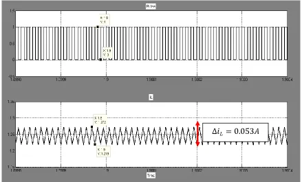
[image:57.612.84.523.133.398.2]below. The current ripple, calculated is of (1.272A-1.219A) = 0.053A
Figure 4.9: Graph of pulse with a frequency, f of 80 kHz and the current ripple, at the
4.3.2 Case 2: The effect towards current ripple when the value of duty cycle is varied
The next case is to see the effect of varying the duty cycle towards the current ripple.
Table 4.3 is the parameters used in circuit figure 4.10 below. The parameters are remained
constant as the previous case (varying the value of frequency) whereby only the duty cycle
varies. This part will show the result of current ripple at the inductor, ΔiL (A) for duty cycle
ranging from 10 % to 90%. Figure 4.10 as shown below is the graph of pulse with a duty cycle
of 10% and the characteristic of the current ripple at the inductor obtained from the output of
the scope that is tapped at the inductor as shown in figure 4.1 above. For a duty cycle of 10%,
the time on of the pulse generated is only 10% of the total time or period of the pulse causing
the current to charge at a short period and discharge at a longer period. The current ripple,
calculated is of (0.3905-0.3487) = 0.0418A
Figure 4.10: Graph of pulse with a duty cycle, D of 10% and the current ripple, at the
Figure 4.11: Graph of pulse with a duty cycle, D of 20% and the current ripple, at the
inductor
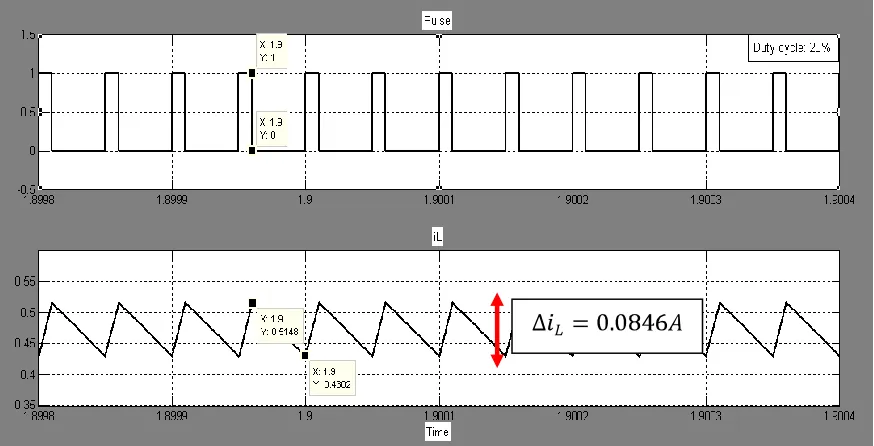
The current ripple, calculated for figure 4.11 with a duty cycle of 20% above is
[image:59.612.96.533.71.294.2]of (0.5148-0.4302) = 0.0846A
Figure 4.12: Graph of pulse with a duty cycle, D of 30% and the current ripple, at the
For a duty cycle of 30%, the current ripple in the inductor for a duty cycle of 30% based on
the simulation done in the MATLAB simulink software, is shown in figure 4.12, the minimum
current, Imin is 0.5603A and the maximum current, Imax is 0.6887A which result of a
of (0.6887A-0.5603A) = 0.1284A. As for a duty cycle of 40% shown in
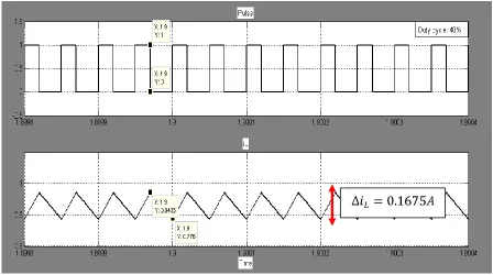
[image:60.612.85.533.195.445.2]figure 4.13 below, the of (0.9435A-0.776A) = 0.1675A
Figure 4.13: Graph of pulse with a duty cycle, D of 40% and the current ripple, at the
Figure 4.14: Graph of pulse with a duty cycle, D of 50% and the current ripple, at the
inductor
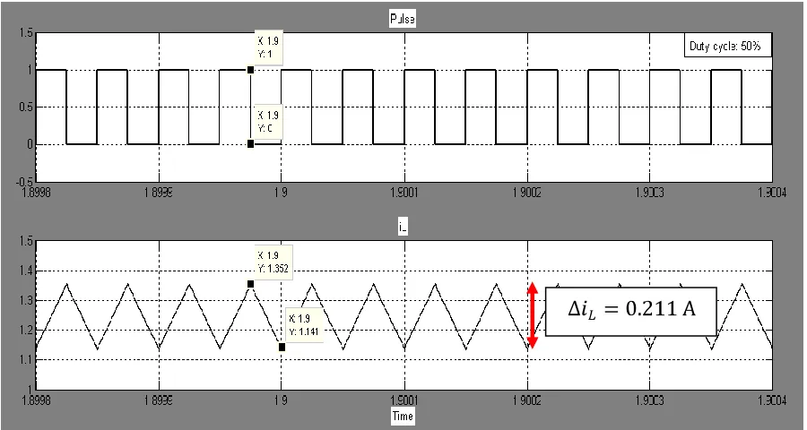
As shown in figure 4.14 above, since the duty cycle is 50%, the time on and the time off of the
pulse (switching) is the same. The calculated is = (1.352A-1.141A) =
0.211A. Figure 4.15 below shows the characteristic of the current ripple of 60% duty cycle.
The time on is longer than the time off which means the time for the inductance to charge is
longer than for it to dissipate its energy. the current ripple obtained is =
Figure 4.15: Graph of pulse with a duty cycle, D of 60% and the current ripple, at the
inductor
Figure 4.16: Graph of pulse with a duty cycle, D of 70% and the current ripple, at the
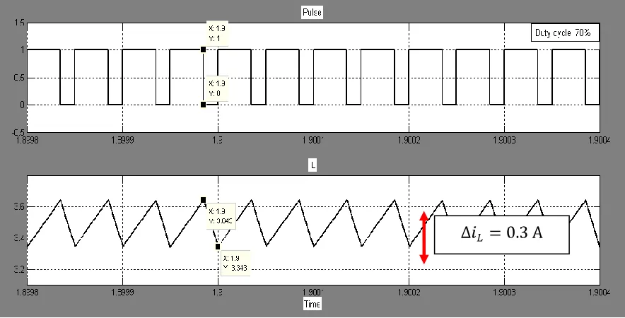
[image:62.612.92.534.397.622.2]Up to 70%, it is noticed that as the higher the duty cycle, the larger the current ripple. The
current ripple for 70% is = (3.643-3.343) = 0.3A as shown in figure 4.16
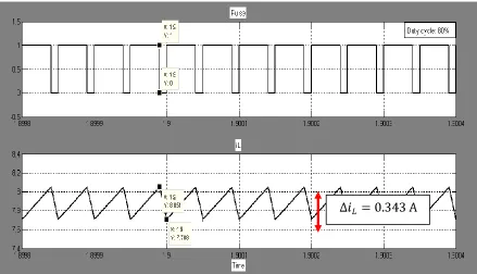
[image:63.612.90.529.153.405.2]above. As for a duty cycle of 80% in figure 4.17, the is (8.051-7.708) = 0.343A.
Figure 4.17: Graph of pulse with a duty cycle, D of 80% and the current ripple, at the
inductor
For the last parameter for the response of the current ripple towards the change of duty cycle is
shown in figure 4.18 below. The figure 4.18 below shows that the time off for the switching is
too brief. The same parameter will be tested in the experimental part to discover either does
the experimental and simulation part differs. The can be calculated as =
Figure 4.18: Graph of pulse with a duty cycle, D of 90% and the current ripple, at the
4.3 Experimental Results
The circuits are checked before connecting all the circuits as in figure 4.19 (boost
[image:65.612.121.527.161.439.2]circuit, gate drive, DSP), load and inductor together.
Figure 4.19: Setup of the boost circuit
The pulse width modulation (PWM) done in the code composer studio is uploaded into
the DSP and the output of the DSP (connector P8 pin 15 as attached in Appendix D) is
connected to the oscilloscope’s probe. This is to recheck that pulse that is created in the
coding. The PWM coding is attached in appendix E. By adjusting and changing the T1PR (for
frequency and T1CMPR for duty cycle, the change of the pulse at the oscilloscope is
monitored. The pulse obtained at the output is based on the setting of the T1PR and T1CMPR.
Both commands are placed at the output window as shown in figure 4.20: Output window in
the Code composer studio (CCS) and the system is set to continuous refresh so that both
commands T1PR and T1CMPR can be edited at will. Figure 4.21 below is the illustration on
the relationship of the T1PR and T1CMPR in the process of varying the frequency or duty
Figure 4.20: Output window
Figure 4.21: Relationship of T1PR command and T1CMPR command
As the output of the PWM is satisfied, the DSP is connected to the gate drive circuit
with an input source of 5V. The output of the gate drive optocoupler (pin 5 and 8) is checked
to have an output of 15V. This is necessary to ensure that the pulse from the gate drive is able
to drive the IGBT according to the pulse. The pulse from the IGBT is connected to the
oscilloscope to see its output. The boost circuit is then connected to the amplified pulse from
the gate drive circuit. The input source of the boost circuit is set to 12V and a multimeter is T1CMPR
T1PR
Pulse
used to check the output of the boost circuit. With a duty cycle of 50%, the output of the boost
circuit must be twice the value of the input which is 24V.
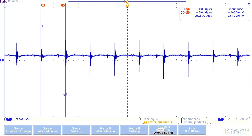
The probe from the oscilloscope is then connected in series with the inductance to see the
current ripple. Unfortunately, the current ripple is too small it is not visible at the oscilloscope
[image:67.612.83.525.199.438.2]as stated in figure 4.22: Current ripple below.
Figure 4.22: Current ripple
Based on the output in figure 4.22: Current ripple above, modification is done to the
circuit where a current transducer is added into the circuit. The current transducer is used to be
able to sense signals or measurements that falls outside ranges. With the addition of the
current sensor, the ranges that are unavailable to obtain with common requirements, can be
detected and diagnose. The calibration is done between the current sensor and the oscilloscope
as the whereby, 100mV per division in the oscilloscope is equal to 500mA or in other words, it
is with a ratio of 1:5. The datasheet of the current transducer is attached in Appendix F. Once
the modified circuit is reconnected, the output at the oscilloscope is obtained as will be
4.3.1 Case 1: The effect towards current ripple when the value of frequency is varied
As shown in figure 4.10 the experimental result of varying the value of frequency (10 kHz) for
the boost circuit is captured and saved using the oscilloscope. The result as stated at the upper
right corner of the result is in mV. Since the configuration scale set between the current
transducer and the oscilloscope is 100mV/div for every 500mA (1:5m), the amount of mV
needs to be converted into the actual value (in current, A). The current transducer is used to
magnify the result obtained (to enlarge the scale) so that the output can be monitored and seen
at the oscilloscope as well for galvanic isolation between the primary and the secondary
circuit. Based on the result in figure 4.23 below, the current ripple, from Eq. (2-3) when
the frequency is 10 kHz is with a maximum current, Imax of 1.29A and a minimum current,
[image:68.612.104.548.336.624.2]Imin of 0.87A thus the is ( ) =
Figure 4.23: Pulse with a frequency, f of 10 kHz and the current ripple, iL at the inductor Vout=22V
The process of the charge and discharge of the current at the inductor is depending on the pulse
The result shown in figure 4.24 is the result when the frequency of the boost converter is set to
[image:69.612.86.556.123.408.2]20 kHz. The current ripple obtained is ( ) =
Figure 4.24: Pulse with a frequency, f of 20 kHz and the current ripple, iL at the inductor
As can be seen in figure 4.25 below, the Imax is and the Imin
is . Therefore, the is 0.165A
Vout=22V
The process of the charge and discharge of the current at the inductor is depending on the pulse
Figure 4.25: Pulse with a frequency, f of 30 kHz and the current ripple, iL at the inductor
As for figure 4.26 below, when the frequency is increased to 40 kHz, the switching process
would be faster in a second. in figure 4.26, the minimum current is 1 A and the maximum
current is 1.15 A resulting of a current ripple, of 0.15A. Vout=22V
The process of the charge and discharge of the current at the inductor is depending on the pulse
Figure 4.26: Pulse with a frequency, f of 40 kHz and the current ripple, iL at the inductor
The frequency of the boost converter is added again to 50 kHz as illustrated in figure 4.27
below causing the switching process of the boost converter even faster. The current ripple
Figure 4.27: Pulse with a frequency, f of 50 kHz and the current ripple, iL at the inductor
Figure 4.28: Pulse with a frequency, f of 60 kHz and the current ripple, iL at the inductor
As can be seen in figure 4.29, the circuit is tested with a frequency of 70 kHz. The minimum
current, Imin is 1.115A and the maximum current, Imax is 1.08A resulting of a current ripple
of = 0.035A. The circuit is then tested with a frequency of 80 kHz. When the frequency is
increased, a buzzing sound starts to erupt. Since an unfamiliar sound is heard, the experiment
4.4.2 Case 2: The effect towards current ripple when the value of duty cycle is varied
As can be seen in figure 4.3, with a duty cycle of 10%, the turn on state is only for a
brief second while the turn off state is longer. The current ripple is with a ΔiL of 0.048 A.
Figure 4.31 below shows a Pulse with a duty cycle, D of 20% and the current ripple, iL at the
[image:75.612.85.545.235.496.2]inductor is ΔiL=0.095 A.
Figure 4.30: Pulse with a duty cycle, D of 10% and the current ripple, iL at the inductor
Figure 4.31: Pulse with a duty cycle, D of 20% and the current ripple, iL at the inductor
Figure 4.32 below shows the effect of current ripple when the duty cycle is 30%. The current
ripple is ΔiL= 0.14A.
Figure 4.33: Pulse with a duty cycle, D of 40% and the current ripple, iL at the inductor
As the duty cycle increases, the on state also increases. The charging of the current during the
on state increases linearly. The current ripple ΔiL= 0.18A. As for a duty cycle for 50% as illustrated in figure 4.34 below, the current ripple also increase. The current ripple ΔiL for a
Figure 4.34: Pulse with a duty cycle, D of 50% and the current ripple, iL at the inductor
Figure 4.35: Pulse with a duty cycle, D of 60% and the current ripple, iL at the inductor
Another 10% of duty cycle is increased as in figure 4.36 causing the duty cycle to be 60% of
[image:78.612.82.545.375.640.2]4.37 with a duty cycle of 70% and 80% the ΔiL with a duty cycle of 70% is 0.5A and the ΔiL
[image:79.612.86.550.121.387.2]for a duty cycle of 80% is 0.39A. as the duty cycle increases, so does the current ripple.
Figure 4.36: Pulse with a duty cycle, D of 70% and the current ripple, iL at the inductor
[image:79.612.87.545.444.695.2]4.4 Chapter summary
Chapter 4 is the results obtained from three methods on determining the effect of
varying the duty cycle and the frequency towards the current ripple of the boost converter.
Based on the result obtained, the higher the frequency, the lower the current ripple in the
inductor but as for the duty cycle, the higher the duty cycle, the higher the current ripple in the
boost converter. The analysis of the results obtained is discussed in the next chapter which is
CHAPTER 5
ANALYSIS AND DISCUSSION
5.1 Introduction
Chapter 5 is where the analysis and discussion takes part. In this chapter, all the data
for calculation, simulation and hardware is compared by placing all the values into a table thus
it is being discussed and analyzed. It can be categorized into two cases which is case 1:
Monitoring and analyzing the effect of the current ripple by varying the value of frequency
and case 2: Monitoring and analyzing the effect of the current ripple if the value of duty cycle
is varied. The result of calculation, simulation and experimental of both cases are discussed.
5.2 Analysis
5.2.1 Analysis on the effect towards the current ripple when varying the value of frequency
Table 5.2 shows the result of current ripple at the inductor, ΔiL (A) for calculation,
simulation and experimental for frequency ranging from 10 kHz to 80 kHz. The frequency is
varied by changing the T1PR command at the watch tab to 10 kHz, 20 kHz, 30 kHz, 40 kHz,
50 kHz, 60 kHz, 70 kHz and 80 kHz while maintaining the duty cycle to be 50%. All the
data’s are recorded. Based on the results obtained in table 5.2 it can be seen that as the
frequency increases, the current ripple decreases. The calculation, simulation and experimental
result values differ but are acceptable as all three results differ in an acceptable range. For
simulation, the values are different than calculation is because of the type of solver used for
Different type of solver would result differently. The relative tolerance set to the simulink
would also be the cause of the differences of value. As for the experimental part, the result
differ from the calculation as the components is not ideal since each components has its own
tolerance as well as other factors that affect the circuit such as voltage drop and losses during
the switching process. Even so, all three methods, calculation, simulation and experimental
[image:82.612.102.522.279.502.2]shows the same pattern whereas, the higher the frequency, the lower the current ripple.
Table 5.1:ΔiL (A) for calculation, simulation and experimental when varying the value of
frequency
In the experimental part of the project, the graphs obtained are captured and saved
from the oscilloscope. The result as stated at the upper right corner of the result graph is in
mV. Since the configuration scale set between the current transducer and the oscilloscope is
100mV/div for every 500mA (1:5m), the amount of mV needs to be converted into the actual
value (in current, A). The current transducer is used to magnify the result obtained (to enlarge
the scale) so that the output can be monitored and seen at the oscilloscope as well for galvanic
isolation between the primary and the secondary circuit.
Frequency (kHz) ΔiL (A):
Calculation
ΔiL (A):
Simulation
ΔiL (A):
Experimental
10 0.428 0.421 0.42
20 0.214 0.211 0.24
30 0.143 0.143 0.165
40 0.107 0.108 0.145
50 0.0857 0.062 0.125
60 0.0714 0.061 0.105
70 0.0612 0.057 0.085