361
NEW MODIFIED ELMORE DELAY MODEL FOR
RESISTANCE-CAPACITANCE-CONDUCTANCE (RCG)
INTERCONNECT NETWORK SCHEME
R.UMA1, I.KRISHNAPPRIYA2, P.DHAVACHELVAN1
1Department of Computer Science, School of Engineering, Pondicherry University, Pondicherry,
India
2Department of Electronics, School of Engineering, Pondicherry University, Pondicherry, India
E-mail: 1
[email protected]
,
2 [email protected]ABSTRACT
This study presents a simple close-form delay estimate, based on first and second order moments that handle arbitrary voltages and conductance effects for a lumped and distributed line. This model introduces a simple tractable delay formula by incorporating conductance (G) into RC network by preserving the characteristics of the Elmore delay model. The accuracy of the interconnect delay estimates can be improved by deploying the conductance effect. This study proves that the proposed model attains quick steady state condition by incorporating the conductance in a RC network thereby reducing the delay in interconnects. The analysis is validated through extensive simulations on a 250 nm CMOS technology. The SPICE simulation shows the overall figure of merit has an improvement of at least 28% when compared to RC Elmore Model and existing RLC interconnect scheme.
Keywords: Elmore Delay, RCG Interconnect, RLC Network, Figure Of Merit, Damping Ratio
1. INTRODUCTION
Interconnects are used to connect components on a chip and it constitute to be a dominant source of circuit delay for modern chip designs. They are typically modeled as RC circuits and RLC circuits based on the studies of the delay models all of which aim at more accuracy with less computational effort.
The traditional approach to determine the signal delay for both analog and digital circuits has been estimated using Elmore delay (also called classical delay model). But this model provides limited accuracy and limited to estimate the delay of the circuit for only step inputs. These issues has been surmounted by incorporating a compound interest problem to the existing Elmore delay to improve the efficiency of the RC interconnect scheme.
The RC interconnect approach has been reported by [1], this approach improves the signal delay, albeit this scheme has been applicable for RC network alone. In [2] reported a closed transfer function method to find the delay estimates using an arbitrary RC with classical Elmore model. This model provides delay accuracy to the first order RC network.
The model proposed in [3] developed a simple closed-form delay estimate, based on first and second moments, which considers the effect of inductance. Using this model significant accuracy in delay can be obtained but applied only for step type signals. The primary issue in this model is; inefficient in calculating the time response of under damped conditions when the interconnect network grows linearly. This issue has been surrogated by the model developed by Y.I. Ismaiel [4]. Their model deals with closed form of RLC network which finds the delay for both damping and under damping response of RLC network when there is linear progression in the interconnection occurs. But the primary constraint in this model is second order approximation is complex for RLC nodes.
Abou-Seidoet [7] proposed a new interconnect delay model named Fitted Elmore Delay (FED) using curve fitting technique. Determinations of curve fitting coefficients are much complicated for larger RC networks. Interconnects are also modeled using S-parameter by estimating series impedance and parallel admittance using telegraph equations has been proposed by [8]. This approach finds suitable only for smaller interconnects.
The model proposed by [9] evaluates the performance of interconnect by deploying the property of conductance to improve the characteristics properties of delay. It is limited for lumped model and step input. A delay model for RLC trees based on algebraic equations and an algorithm has been proposed based on the lie formula Sourajeet Roy [10]. Though the model can be applied to step and ramp input type of signals, it is inefficient for second order delay modeling and limited to only first two circuit moments.
Moment based Delay Modeling for On-Chip RC Global VLSI Interconnect were also introduced by developing Two pole RC model based on first, second and third moment effect into the delay estimate for interconnect lines [11]. This model takes higher order circuit moments for accuracy in delay, but it is not applicable for second order systems. ABCD matrix delay model has been developed by [12] which are used for calculating the Delay by finding first two circuit moments with ABCD matrix. Each interconnect lines is modeled with ABCD matrix. The total delay is divided into two: transport delay and interconnect rise time delay. As Transport delay is included, the delay and rise time delay is more accurate than other model and inductance effect is also considered but in terms of circuit moments it is not more efficient.
The literature survey reported in this study focus only on the interconnect delay model involving resistance, capacitance and inductance effects. But as the technology scales down the significant of conductance plays a vital role for improving the device performance as well as in delay aspect. This study presents a new modified Elmore model (MEDL) which incorporates the effect of conductance to improve the delay for lumped and distributed interconnect networks.
2. MATERIALS AND METHODS
Elmore delay model (EDM) has been widely employed to approximate the interconnect delays in the performance driven analog and digital very large scale integration (VLSI) devices. This
delay model estimates the first moment of the impulse response using a simple closed form expression in terms of design parameter like resistance and capacitance used in the interconnect scheme. This interconnect delay models a wire as a segment of resistance and capacitance which is connect in series as shown in Fig. 1. For lumped model the delay of the circuit is directly proportional to its resistance (R) and capacitance (C). For distributed network with a segment i, the resistance Ri proportional to its length, width of the
wire and ρ resistivity of the sheet.
The delay for a lumped RC interconnects is modeled as the time constant (τ) of an RC interconnect. So the delay for a lumped RC interconnect is
τ= RC (1)
The delay for the distributed RC interconnect is modeled as the total sum of the delay in each node
Delay at node 1 (N1) : τ1= R1C1 (2)
Delay at node 2 (N2) : τ2= (R1+ R2)C2 (3)
Delay at node 3 (N3) : τ3= (R1+ R2+R3)C3 (4)
In general the delay for the distributed RC network is calculated as
n C n R R
R
C R R R C R R C R n
) ... 2 1
( 3
) 3 2 1 ( 2 ) 2 1 ( 1 1
+ + +
+ + + +
+ = τ
(5) If R1=R2….Rn=R and C1=C2…Cn=C ,
then the delay is modeled as
nRC RC
RC
n = +2 +...
τ (6) The Elmore delay equation explains the delay from input to output of the input signal, which is of a step function type. If the step response of the RC circuit is h (t), 50% point delay of the monotonic step response is the time τn that satisfies the above
363
-
+
V
R1 L1
C1
N1 R2 L2
C2
N2 R3 L3
C 3 N3
-
+
V (a)
(a)
To achieve higher accuracy, a two-pole model which is based on RLC interconnects are employed to estimate the delay. The model is based on the first two moments. The delay model gains higher accuracy than RC due the second moment capturing effect of the inductance. Recently, metrics for RLC interconnects have been proposed based on the first three central moments [R. Gupta et al; 1997] [13]. These three central moments are used to detect underdamping condition and control of inductance effects. The lumped and distributed RLC model is shown in Fig. 2.
The delay for a lumped RLC interconnects is modeled as the time constant of an RLC interconnect. So the delay for a lumped RLC interconnect is
τ= 2L/R (7) The delay of the distributed RLC interconnect is modeled as the total sum of the
delay in each node
(8) The major drawback of RLC models are: these interconnect schemes responds to step input and does not characterize the overshoots and settling time of an under damped response. Furthermore, three different equations has to be formulated to calculate the real, complex and
multiple poles. Moreover the characteristics of RLC
(b)
(b)
(b)
model does not focuses to closed-form solutions for the moments of a interconnect tree. The other draw backs of inductive RLC circuit are: extracting the inductance is in general a 3-D problem and is extremely time consuming for complex geometry. Generally inductance depends on the entire current loop therefore it is impractical to extract the inductance from the chip layout. The primary focus of this study is to introduce a simple tractable delay formula for RCG network preserving the characteristics of the Elmore delay model with improved accuracy in the interconnect delay scheme (model).
3. PROPOSED RCG DELAY MODEL
This study presents a simple close-form delay estimate, based on first and second order moments that handle arbitrary voltages and conductance effects for a lumped and distributed line. This model introduces a simple tractable delay formula by incorporating conductance (G) into RC network by preserving the characteristics of the Elmore delay model. This Modified Elmore Delay Model (MEDL) with RCG interconnect considers a uniform wire that is schematized as lumped or distributed RCG network whose total resistance Rtotal = ρL/W and capacitance Ctotal= βLW which is proportional to its length L. The general property of the RCG network is portrayed as:
-
+
V
-
+
V R1
C1 N1
N3
C3 R3
+
V R1
C1 C2
R2
+
V
N1 N2
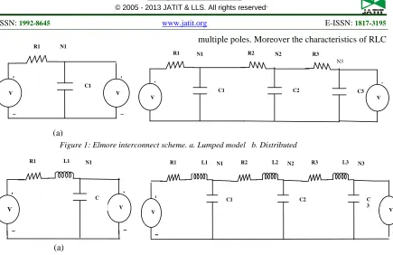
Figure 1: Elmore interconnect scheme. a. Lumped model b. Distributed
-
+
V
R1 L1
C
-
+
V
[image:3.612.94.529.56.338.2]N1
Figure 2: RLC interconnect scheme. a. Lumped model b. Distributed network
2 2 2
2 2 2 2 2 2
....
L R RL L R RL L nR nRL L n
R R R R
-
+
V
-
+
V
R1
C1 G1
-
+
V
-
+
V
R3
G3 C3
R2
G2 C2
R1
G1 C1
[image:4.612.93.537.67.727.2]N1 N2 N3
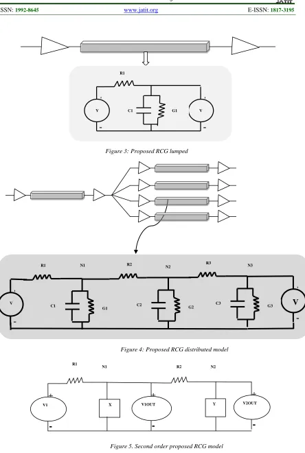
Figure 3: Proposed RCG lumped
Figure 4: Proposed RCG distributed model
-
+
V1R1
X
-
+
V1OUT Y
R2
-
+
V2OUT
N1 N2
365 • In this proposed model the root node is
connected through drivers (buffers) and there may be several loading capacitances connected along the interconnect network.
• The first moment and the second moment of transfer function from source to sink is calculated using recursive approach (iteration formula)
• The interconnect network is divided into several segments. Each segment is associated with a series resistance and parallel connected capacitance and conductance.
• Resistance along each segment i related to, Ri ∝
1/wi, where wi→ width of the wire along i th
segment.
• Capacitance along each segment i related to, Ci ∝ wi , where wi→ width of the wire along i
th
segment.
• Conductance along each segment i related to, Gi
∝ wi/Li, where wi→ width of the wire along ith
segment, Li→ length of the wire along ith
segment.
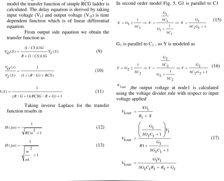
The delay estimates for lumped network is shown in Fig. 3. To estimate the delay of lumped model the transfer function of simple RCG ladder is calculated. The delay equation is derived by taking input voltage (VI) and output voltage (VO) is time
dependent function which is of linear differential equation.
From output side equation we obtain the transfer function as
Taking inverse Laplace for the transfer function results in
Where 1 (R G)
RCG
ω = +
( )
RCG R G
τ =
+ is the change in output voltage VO(t)
is delayed by the time constant.
( )
RCG
R G
τ =
+ (14)
Fig. 4. Shows the proposed distributed model. For distributed network the entire interconnect is divided into various segments. Each segment consists of series resistance and parallel connected capacitance and conductance. First the transfer function of the ladder is estimated with single resistance (R), capacitance (C) and conductance (G). Then using the recursive node approach, the next segment delay is calculated using the preceding and successive node. This process is continued till the last segment of interconnect network and the transfer function is applied between the source and the sink. The delay estimate for the distributed network is shown below In second order model Fig. 5, G1 is parallel to C1 so for simplification X is modeled as
G2 is parallel to C2 , so Y is modeled as
out
V
1 ,the output voltage at node1 is calculatedusing the voltage divider rule with respect to input voltage applied
(1 / )11
( ) ( )
(1 / )11 CS G
VO S VI S
R CS G
=
+
(9)
( ) 1
( ) (1 ( / ) )
VO s
VI S R G RCS
=
+ +
(10)
1 ( )
( / 1)( / ) 1
H S
R G RCSG R G =
+ + + (11)
1 ( ) 2 1 H j RC ω ω = +
(12) 1 ( ) 2 1 1 H jω ω ω = + (13) 1
1 1 1
|| 1
1 1
1 1 1
1 1
G
SC G
X G X X
SC SC G
G SC = ⇒ = ⇒ = + +
(15) 2
1 2 2
||
2 1
1
2 2 2
2 2 G
SC G
Y G Y Y
SC SC G
G SC = ⇒ = ⇒ = + +
(16) 1 1 1 1 1 1 1 1 1 1 1 1 1 1 1 1 1
1 1 1 1 1
XV V out R X G V SG C V out G R SG C G V V out
SG C R R G
= + + = + + = + +
(17) [image:5.612.76.533.373.742.2]out
V
2 , the output voltage at node2 is calculated using the voltage divider rule with respect to input voltage appliedThe closed loop transfer function of a second order system can be written as
By comparing the above equation with the characteristic equation, which is given in the form
2 2
2
n n S +
ξω
+ω
We obtain the values of
ω
n &ξ
Where
ω
n is the natural frequencyξ
is the damping ratio, is a parameter characterizesthe frequency response of a second order ordinary differential equation and it is a measure of how rapidly the oscillations decay from one bounce to the next. When
ξ
value is zero the system remains undamped and when it is less than 1 the system is said to be underdamped , whereas the value is greater than 1 , then the system said to be overdamped condition when it is equal to 1 it is in critically damped condition.The delay can be calculated from the below equation
n
ξω
τ
= 12 2 2 2 1 1 1
( ) ( )
2 2 2 1 1 1 1 1 2 2
R C G R C G
R C G R G R C G R G
τ =
+ + +
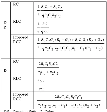
[image:6.612.311.522.264.486.2](22) The above derived equation is the delay equation of the second order MEDL model. The damping ratio and delay expression for the proposed RCG MEDL, RC and RLC interconnect scheme is shown in Table 1.
Table 1: Damping ratio and Delay for RC , RLC and Proposed RCG
4. SIMULATION RESULTS
The proposed model is simulated using simulation tool TANNER ASIC-EDA tool in order to compare the results in terms of delay and power. The model is simulated by taking typical values of resistance R= 10k, capacitance C=1pf and conductance G=0.1M for lumped and distributed interconnects. Buffers are inserted into RCG lines to partition an interconnect line into shorter sections and for signal integrity, thereby reducing the total propagation delay and the corresponding rising time, fall time are calculated. Input signal is unit step signal and the delay estimates refer to 50% threshold voltage. In this experiment, simulations are performed for RC and RLC for distributed and lumped and its performance are compared with proposed model. The interconnect dimension are taken for 0.250 µm technology with
2 2
1
2 1 1
1
2 2 1 1 1 1 1
2 2 2 1 2 2 YV in V out R Y
G G V
SC G SG C R R G V out G R SC G = + + + + = + +
(18)
(
)(
)
2 1 2
1 2 2 2 2 2 1 1 1 1 1
V out G G
V SR C G R G SG C R R G
= + + + + 1 2 ( ) 2 ( )
1 1 1 2 2 2 2 2 2 1 1
( ) ( ) )
1 1 1 2 2 2 2 1 1
G G H S
S G C R G C R SR C G R G
SG C R R G R G R G =
+ +
+ + + + + +
1
1 1 2 2 ( )
( ( ) ( ))
2 2 2 2 1 1 1 1 1 2 2
2 2 2 1 1 1
( 1 1)( 2 2)
2 2 2 1 1 1 C R C R H S
S R C G R G R C G R G S
R C G R C G
R G R G
R C G R C G = + + + + + + + (19)
( 1 1)( 2 2)
2 2 2 1 1 1
R G R G
n
R C G R C G
ω = + + (20)
( ) ( )
1 2 2 2 1 1 1 1 1 2 2
2 2 2 2 1 1 1( 1 1)( 2 2) R C G R G R C G R G
R C G R C G R G R G
ξ = + + +
+ + (21) D R
RC
1 1 1 2 2
2 1 1 2 2 R C R C
R C R C + RLC 1 2 RC LC Proposed
RCG 1 2 2 2( 1 1) 1 1 1( 2 2) 2 2 2 2 1 1 1( 1 1)( 2 2)
R C G R G R C G R G
R C G R C G R G R G
+ + +
+ +
D
RC 2 2
1 1 2
1 1 2 2 R C R C
R C +R C
RLC
2LC
RC Proposed
RCG 2 2 2 2 1 1 1
( ) ( )
2 2 2 1 1 1 1 1 2 2 R C G R C G
R C G R +G +R C G R +G
367 Table 2: Delay obtained for Various R, C and G for
lumped model
Table 3: Delay obtained for Various R, C and G for distributed model
Proposed RCG
RLC
[image:7.612.128.465.246.377.2]RC Input
Figure 6: Simulation results proposed RCG lumped model
Proposed RCG
RLC
RC
Input
Figure 7: Simulation results proposed RCG distributed model
R (kΩ)
C (pf)
G (mS)
Theoretic al Delay (nS)
Simula ted Delay
(nS)
10 1 0.1 5 5.5769
8 4.44 4.6071
6 3.75 3.3251
4 2.8571 3.0656
2 1.666 1.8939
1 0.9090 1.1197
10 2 0.1 10 10.819
4 20 21.350
6 30 29.447
8 40 36.710
10 50 47.024
10 1 0.09 5.26 5.5997 0.08 5.55 5.6252 0.07 5.88 5.3587 0.06 6.24 5.3839 0.05 6.66 5.5531 Remarks: Simulated delay time=time difference between input transition (50% level) and the 50% output level .The theoretical values are obtained through equation (14)
R= Resistance, C=capacitance, G=conductance
R1=R2
(kΩ)
C1=C2
(pf)
G1=G2
(mS)
Theoreti cal Delay (nS)
Simulate d Delay (nS)
10 1 0.08 5 10.688
8 4.44 8.6561
6 3.75 6.6673
4 2.85 5.3331
2 1.666 3.7349
1 0.9090 2.9631
10 2 0.08 10 19.086
4 20 38.367
6 30 51.333
3 40 29.786
5 50 46.515
10 1 0.07 5.88 10.133
[image:7.612.314.509.436.664.2]minimum cross-section of 0.33µm and 0.18µm. The time response for lumped and distributed interconnect scheme is shown in Fig. 6 and 7 . The time response is analyzed for the step response of 200ns with input voltage of 5v and output response obtained is an exponential curve. From this experimental setup it is noticed that the output response is faster for the proposed RCG interconnect scheme. Table 2 and 3 shows the delay parameter obtained through simulation and theoretical values for different values of R, C and G for lumped and distributed model
Table 4 presents the simulated results for power and figure of merit obtained for various voltages keeping R, C and G as constant. For this observation R value is taken as 10kΩ and C value is 1pf and conductance is 0.1mS. The figure of merit defines the relative utilization to characterize the performance of a device. This parameter is obtained by taking the product term of propagation delay and the average power dissipation. In this experiment the minimum voltage
Interconnect scheme
Type of interconnect
Voltages (v)
delay (ns)
Rising time (ns)
Fall time (ns)
Power
(μw) Figure of merit x10-6 lumped
model
RC [1] 2 7.6074 0.7351 0.5078 0.477 3.628
2.5 7.3844 0.5960 0.4238 0.479 3.537
3.3 7.8278 0.5961 1.2514 0.474 3.710
4.2 7.5788 0.4742 2.1319 0.469 3.554
5 8.5908 1.2430 2.5253 0.456 3.917
RLC [3] 2 7.6066 0.7286 0.5068 0.477 3.628
2.5 8.0121 0.5961 1.2514 0.474 3.797
3.3 7.8809 0.7625 1.8254 0.468 3.688
4.2 7.5768 0.4714 2.1312 0.469 3.553
5 8.5446 1.2353 2.5249 0.456 3.896
RCG[prop] 2 6.0466 2.7260 0.2420 0.473 2.860
2.5 4.6493 2.2437 1.0272 0.464 2.157
3.3 5.2921 1.4797 0.2300 0.464 2.455
4.2 4.5972 2.1390 0.2595 0.474 2.179
5 5.5769 2.6508 2.1005 0.455 2.537
distributed model
RC [1] 2 16.225 0.6935 0.9249 0.476 7.723
2.5 15.613 0.5661 1.1233 0.473 7.384
3.3 15.502 0.6918 1.6364 0.467 7.239
4.2 15.315 0.6740 1.8890 0.470 7.198
5 16.712 0.6837 1.1882 0.476 7.954
RLC [3] 2 16.280 1.1090 0.9210 0.477 7.765
2.5 15.580 0.5791 1.1212 0.473 7.369
3.3 15.911 0.5184 0.3181 0.475 7.557
4.2 15.304 0.6659 1.8864 0.469 7.177
5 16.060 1.1624 1.1162 0.476 7.644
RCG[prop] 2 9.7487 1.8991 0.9536 0.457 4.455
2.5 9.9506 0.8327 0.2690 0.470 4.676
3.3 10.646 0.8682 0.2096 0.468 4.982
4.2 9.645 1.3236 0.2594 0.473 4.562
5 10.688 1.1482 0.6042 0.455 4.863
Remarks:
rising time=time for a waveform to rise from 10% to 90% of its steady-state value. falling time= time for a waveform to fall from 90% to 10% of its steady-state value. Power reported is an average power
Figure of Merit has been calculated by the taking the product term of delay and average power consumption. The interconnect scheme is simulated for fixed values of R, C and G. R=10kΩ, C=1pf, G=0.1mS
369 taken for this analysis 2V and the maximum of 5V. The rise time is calculated for a waveform to rise from 10% to 90% of its steady-state value. The fall time is calculated for a waveform to fall from 90% to 10% of its steady-state value. Table 5 elucidates the percentage improvement in delay, power and figure merit for the proposed RCG interconnect scheme with respect to existing RC and RLC interconnect scheme.
5. DISCUSSION
A new interconnect scheme RCG model and is performance issues are presented. The
proposed RCG model performs better than its existing counterparts. Table 5 depicts the
percentage of improvement in delay, power and figure of merit of proposed interconnect with respect to RC and RLC for lump and distributed models. The analysis of the proposed study illustrates progressive improvements with RC and RLC in terms of delay, power and figure of merit. From Table 5 it is noticed that the percentage of delay is much improved for RC model than RLC interconnect model. For the lumped RC model with minimum voltage of 2V, the delay factor has improved to 21% and 40% improvement when the supply voltages reaches 4V keeping all the values of R, C and G as constant. Similarly for distributed network there is 40% improvement attained for the input voltage of 2V to 5V. For RLC lumped model
Overall improvement with respect to Proposed RCG in terms of different
voltages
Interconnect scheme Voltages (v)
% improveme nt in delay
% improveme
nt in power
% improvement in figure of
merit
Lumped model w.r.t RC 2 20.51 0.83 21.16
2.5 37 3.13 39
3.3 32.39 2.1 33.82
4.2 39.34 -1.06 38.68
5 35 0.2 35.23
Lumped model w.r.t RLC 2 16.53 0.83 21.16
2.5 41.97 2.1 43.98
3.3 32.84 0.4 33.43
4.2 39.32 -0.5 38.67
5 34.73 0.21 34.88
Distributed model w.r.t RC 2 39.91 3.99 42.31
2.5 36.26 0.63 34.56
3.3 31.32 -0.21 31.17
4.2 37.04 -0.63 36.62
5 36.04 4.41 38.86
Distributed model w.r.t RLC 2 40.11 4.19 42.62
2.5 36.13 0.6 36.54
3.3 33.09 1.47 34.07
4.2 36.97 -0.85 36.43
[image:9.612.158.464.144.545.2]5 33.44 4.41 36.38
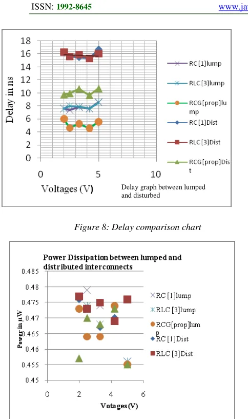
Figure 8: Delay comparison chart
Figure 9: Power comparison chart
Figure 10: Figure of merit comparison chart
the minimum improvement is 16% to a maximum of 40%. When comparing the power aspect, for certain voltages there was no improvement which is indicated in negative sign. For figure merit the minimum improvement is 21% which is obtained for lumped RC with the voltage of 2V and maximum improvement of 43% for lumped RLC model for the supply range of 2.5V.
Fig.8 shows the delay chart for proposed and existing interconnect scheme for different voltages. For the minimum supply voltage of 2V the delay factor for RC [1] lumped is 7.6074ns, for RLC [3] lumped is 7.6066ns and for the proposed model the delay factor is 6.0466ns. Similarly for the maximum of 5V the delay is observed to be 8.5908ns for RC [1] lumped, 8.5446ns for RLC [3] and 5.557ns for the proposed model. So from this analysis it is well tactic that the proposed model performs better than its existing counterparts for the lumped and distributed networks. Fig. 9 depicts the performance of power consumption between RC, RLC and proposed model. Fig. 10 presents the figure of merit comparison chart for the proposed and existing interconnect model.
6. CONCLUSION
This analysis systematically derives closed form delay equation for the proposed RCG interconnect scheme by taking second order moments into account. The simulation results shows the proposed interconnect scheme performance is better than the existing in terms of delay, power and the figure of merit. The performance analysis shows the proposed RCG interconnect scheme has improved in reducing the delay to the maximum of 42 % and 43 % improvement in the figure of merit. The analysis has been done for different voltages by taking different values of R, C and G values. Comparisons on performance analysis shows the RCG interconnect scheme to be more efficient than the existing counterparts. The model proposed suitable for applying in larger circuit will show significant improvement in delay and power.
REFERENCES:
[1] MutluAvci and SerhanYamacli , “An improved Elmore delay model for VLSI interconnects” , Mathematical and Computer Modelling 51 , 908-914 , 2010.
Delay graph between lumped and disturbed
371 [2] Ashis Kumar Mal and AnindyaSundarDhar,
“Modified Elmore Delay Modelfor VLSI Interconnect”IEEE Trans. Comput.-Aided. Des 978-1-4244-7773-9,2010.
[3] A.B. Khang, S. Muddu, An analytical delay model for rlc interconnects, IEEE Trans. Comput.-Aided. Des. 16 (12) 1507-1514,1997. [4] Y.I. Ismail, E.G. Friedman, J.L. Neves,
Equivalent elmore delay for RLC trees, IEEE Trans. Comput.-Aided. Des. Integr. Circuits Syst. 19 (1) 83-97,2000.
[5] Massimo Alioto, “Modeling strategies of the input admittance of RC interconnects forVLSI CAD tools” Microelectronicselsevier Journal 42 (2011) 63–73.
[6] L.T. Pillage, R.A. Rohrer, Asymptotic waveform evaluation for timing analysis, IEEE Trans. Comput.-Aided. Des. Integr. Circuits Syst. 9 (4) (1990) 352-366.
[7] A.I. Abou-Seido, B. Nowak, C. Chu, Fitted elmore delay: a simple and accurate interconnect delay model, IEEE Trans. VLSI Syst. 12 (7) (2004) 691-696.
[8] YungseonEo and William R. Eisenstadt, “High-speed VLSI Interconnect Modeling Based on S-Parameter Measurements” , IEEE transactions on components, hybrids, and manufacturing technology, vol. 16, no. 5, 1993. [9] VikasMaheshwari, Abhishek Sharma, D. Mandal,
R. Kar, A.K. Bhattacharjee, “Transient and delay analysis for on-chip high speed VLSI RLCG interconnection network in 0.18µm technology” , Journal of Electron Devices, Vol. 11, pp. 554-559,2011
[10] Sourajeet Roy and AnestisDounavis, “Efficient Delay and Crosstalk Modeling of RLCInterconnects Using Delay Algebraic Equations”, IEEE transactions on very large scale integration (VLSI) systems, vol. 19, no. 2, 2011
[11] VikasMaheshwari andAlkaGoyal , “Moment based Delay Modelling for On-Chip RC Global VLSI Interconnect for Unit Ramp Input “ Ninth international conference on computer science and software engineering , 2012.
[12] Guofei Zhou, Li Su, Depeng Jin, LieguangZeng, “A Delay Model for Interconnect Trees Based on ABCD Matrix”, IEEE journal 978-1-4244-1922 , 2008.