ISSN(Online): 2320-9801
ISSN (Print): 2320-9798
I
nternational
J
ournal of
I
nnovative
R
esearch in
C
omputer
and
C
ommunication
E
ngineering
(An ISO 3297: 2007 Certified Organization)
Vol. 4, Issue 10, October 2016
A Review of Low Power High Speed Flash
ADC Design Techniques
Chanakya Dharani 1, Ravi J 2
Assistant Professor, Department of ECE, Ekalavya Institute of Technology, Chamarajanagar , Karnataka, India1
Professor Department of ECE, Global Academy of Technology, Bangalore, Karnataka, India2
ABSTRACT: The Data converters are essential interface circuits between the analog world that people live in and the digital processors that people live with. Linearity, which often is a tradeoff against other performance criteria, is one of the major performance demands from applications for both Analog-to-Digital Converts (ADC) and Digital-to-Analog Converters (DAC). There are many types of ADC’s available such as pipeline ADC, successive approximation ADC, delta sigma ADC etc. In present day CMOS technology the flash ADC is composed by utilizing the dynamic method, it reduces the power and delay. A flash ADC is extremely valuable for fastest speed operations when it is compared with the other ADC architectures. Comparator and Encoder are vital part of flash ADC. This paper presents review of Efficient Low Power High Speed Flash ADC Techniques.
KEYWORDS: ADC, Flash ADC, Resolution, Conversion rate, Comparator, Conversion speed, Encoder
I. INTRODUCTION
Mixed signals are wide spread in many applications for example in Audio video etc. Digital receivers for high bit rate communications are spurring on the conversion rate of Analog to- Digital Converters (ADCs). With phenomenal growth of modern communications and signal processing systems, handheld wireless computers and portable electronics are becoming increasingly popular. ADCs are becoming part of System-On-Chip (SOC) instead of a standalone circuit for data converter. The average power consumption and the speed in these applications has become the most critical design concern .To limit energy in a reasonable size battery, minimum power dissipation in the mixed signal integrated circuits is necessary. Although the Flash type ADC design has been widely defined for these applications, and has different architectures, resolutions, sampling rates, power consumptions and a range of operating temperatures. These features available in a Flash ADC are of prime importance. A high trade-off is found among these parameters. The power dissipation increases with the increase in speed and resolution. This results in limitations for Flash ADC at higher resolutions.
II. FLASH ADC WITH QV COMPARATOR
ISSN(Online): 2320-9801
ISSN (Print): 2320-9798
I
nternational
J
ournal of
I
nnovative
R
esearch in
C
omputer
and
C
ommunication
E
ngineering
(An ISO 3297: 2007 Certified Organization)
Vol. 4, Issue 10, October 2016
Figure.1 ADC architecture using the QVC comparator
Encoder is used to change the 1-out-of-n code into a binary code. A new digital encoder network called the Pseudo- dynamic NMOS encoder is used in the QVC based architecture of flash ADC. The Pseudo dynamic NMOS encoder outperforms all of the existing encoding networks. The new encoding network offers high data conversion rate with low power consumption.
III LITERATURE REVIEW
This paper gives survey on various techniques of Flash ADC design. Researchers have implemented flash ADC with different number of bits and different CMOS technologies
Jincheol Yoo et al., [1] this paper presents a new voltage comparator design called Quantum Voltage (QV) comparator for the next generation deep sub-micron low voltage CMOS flash A/D converter (ADC). The new QV comparator has been designed and simulated to verify the low voltage operation. Both the 6-bit QVC flash ADC and the 8-bit QVC flash ADC are correctly operating with high speed and low power consumption. The simulation results with a 0.7 V power supply shows that the QV comparator has a great advantage in power consumption and noise rejection.
Geetanjali Sharma et al., [2] the comparative analysis, we have chalked out the best and worst styles based upon their estimated power consumption, PDP and the area calculation based upon the number of transistors. Seven different approaches to implement a 2 bit magnitude comparator have been discussed below. The best magnitude comparator using Hybrid PTLI CMOS logic style, derived from this analysis has been proposed in this paper.
Megha R and Pradeepkumar K A [3] A 4-bit CMOS based flash ADC is presenting, which uses reduced comparator and multiplexer based architecture. Here both the analog and the digital parts of the proposed ADC are completely modified. This architecture uses only 4 comparators for a 4 bit ADC. This 4-bit ADC is designed and simulated in Hspice with 1.2 V supply voltage.
Ranam Sireesha and Abhishek Kumar [4]The design 4 Bit flash ADC with Using TIQ Technique comparator .TIQ Comparator Compared Input signal with linearity generated switching and produce thermometer code. An efficient thermometer to binary converter has been design using transmission gate based 2:1 multiplexer .This design operated at 800 mv of input frequency 1k Hz .
Liyaqat Nazir et al., [5] new digital encoder network called the Pseudo- dynamic NMOS encoder is proposed to be used in the proposed TIQ based architecture of flash ADC. The 4 Bit Flash ADC is designed using Pseudo dynamic NMOS encoder which out performs all of the existing encoding networks. The new encoding network offers high data conversion at rate of 7 GS/s with low power consumption.
ISSN(Online): 2320-9801
ISSN (Print): 2320-9798
I
nternational
J
ournal of
I
nnovative
R
esearch in
C
omputer
and
C
ommunication
E
ngineering
(An ISO 3297: 2007 Certified Organization)
Vol. 4, Issue 10, October 2016
power reduction compared to a standard domino circuits for 64 bit comparator consumption and also the delay of the circuit simulation
Meghana Kulkarni et al., [18] proposed a FLASH ADC design based on the use of a Quantized Differential comparator. The design has been implemented using TSMC 180nm Technology at MOSIS. The work is an extension of TIQ method which uses systematic sizing of devices in a Conventional CMOS Inverter. The designed ADC has characteristics like Resolution of 6-bit, Power Dissipation of 36.98mW at a power supply of 1.8V.
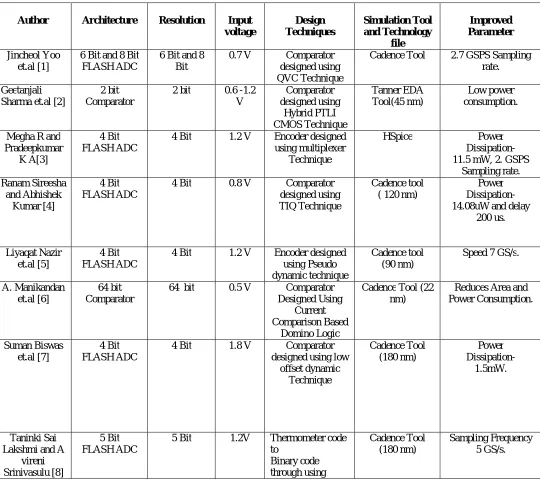
TABLE I RESULT ANALYSIS
The Table 1 shows Result and Analysis’s of different Architecture and Techniques for the following Survey Papers.
Author Architecture Resolution Input voltage Design Techniques Simulation Tool and Technology file Improved Parameter Jincheol Yoo et.al [1]
6 Bit and 8 Bit FLASH ADC
6 Bit and 8 Bit
0.7 V Comparator designed using QVC Technique
Cadence Tool 2.7 GSPS Sampling rate.
Geetanjali Sharma et.al [2]
2 bit Comparator
2 bit 0.6 -1.2 V Comparator designed using Hybrid PTLI CMOS Technique Tanner EDA Tool(45 nm) Low power consumption.
Megha R and Pradeepkumar
K A[3]
4 Bit FLASH ADC
4 Bit 1.2 V Encoder designed using multiplexer
Technique
HSpice Power
Dissipation- 11.5 mW, 2. GSPS
Sampling rate. Ranam Sireesha and Abhishek Kumar [4] 4 Bit FLASH ADC
4 Bit 0.8 V Comparator designed using TIQ Technique
Cadence tool ( 120 nm)
Power Dissipation- 14.08uW and delay
200 us.
Liyaqat Nazir et.al [5]
4 Bit FLASH ADC
4 Bit 1.2 V Encoder designed using Pseudo dynamic technique
Cadence tool (90 nm)
Speed 7 GS/s.
A. Manikandan et.al [6]
64 bit Comparator
64 bit 0.5 V Comparator Designed Using
Current Comparison Based
Domino Logic
Cadence Tool (22 nm)
Reduces Area and Power Consumption.
Suman Biswas et.al [7]
4 Bit FLASH ADC
4 Bit 1.8 V Comparator designed using low
offset dynamic Technique Cadence Tool (180 nm) Power Dissipation- 1.5mW. Taninki Sai Lakshmi and A
vireni Srinivasulu [8]
5 Bit FLASH ADC
ISSN(Online): 2320-9801
ISSN (Print): 2320-9798
I
nternational
J
ournal of
I
nnovative
R
esearch in
C
omputer
and
C
ommunication
E
ngineering
(An ISO 3297: 2007 Certified Organization)
Vol. 4, Issue 10, October 2016
(DCVSL) Technique Anshul Pathak and Shyam Akashe [9] 3 Bit FLASH ADC
3 Bit 0.7V Flash ADC designed using the
Stacked Power gating Technique
Cadence Tool (45 nm) Reduces Leakage power. Vijay V. Chakole et.al [10] 4-bit FLASH ADC
4-Bit 1.8V Encoder designed using MUX based
Technique TANNER tool (180nm ) Input Frequency- 10MHz, SNR- 25.5DB.
Anjuli et.al [11] 2-bit Comparator
2-Bit 0.6 -1.4 V Comparator designed using TG,PTL Technology Tanner EDA (90 nm )
Pseudo NMOS provides least delay amongst all, PTL provides less PDP, Output Swing is better
in CMOS and Transmission Gate design. Kalpana Chaudhary et.al [12] 3-bit FLASH ADC
3-Bit 0.9V Comparator designed using
TIQ technique
Tanner EDA (90 nm )
Leakage Power-18nW, Average Power Consumed- 870μW. Sunghyun Park et.al [13]
4 bit flash ADC
4 bit 1.8 V Designed using Comparator Core
With Inductors Technique
Tanner EDA (180 nm )
Power consumption- 78 mW.
Mingzhen Wang et.al [14]
4 bit flash ADC
4 bit 1.2 V Comparator designed using Timed Digital with
dynamic offset Technique
Tanner EDA (90 nm )
Power consumption- 1.35 m Conversion rate- 2.5GHz. Mamta Gurjar et.al [15]
3 bit flash ADC
3 bit 0.7 V TIQ technique Cadence Tool (45 nm )
Speed-5.3 Gs/s Bandwidth-16.65
MHz. Gulrej Ahmed
et.al [16]
6 bit flash ADC
6 bit 1.2 V Comparator designed using
Variable Switching Voltage CMOS Technique
Cadence Tool (65 nm )
Speed-1 GHz.
S. S. Khot [17] 6 bit flash ADC
6 bit 2.5 V - 3.3 V Comparator designed using TIQ technique Cadence Tool (250 nm)
Speed- 500- 565msps.
Meghana Kulkarni et.al
[18]
6-bit FLASH ADC
ISSN(Online): 2320-9801
ISSN (Print): 2320-9798
I
nternational
J
ournal of
I
nnovative
R
esearch in
C
omputer
and
C
ommunication
E
ngineering
(An ISO 3297: 2007 Certified Organization)
Vol. 4, Issue 10, October 2016
IV. CONCLUSIONS
In this paper different methods of designing flash ADC are examined. Comparator and encoder is vital part of designing Flash ADC. Different methods of designing Flash converter by various authors are compared for performance parameters like power consumption, conversion speed, gain, bandwidth, accuracy, and different technologies employed for obtaining better results.
REFERENCES
[1] Jincheol Yoo, Kyusun Choi, JahanGhaznavi, “Quantum Voltage comparator for 0.07 μm CMOS flash A/D converters”, IEEE Computer Society Annual Symposium on VLSI, pp. 281-281, 2003.
[2] Geetanjali Sharma, Hiten Arora, Jitesh Chawla, and Juhi Ramzai, “Comparative Analysis Of 2-bit Magnitude Comparator using various High Performance Techniques”, IEEE Communication and Signal processing, pp. 0079-0083, 2015.
[3] Megha R, Pradeepkumar K A, “Implementation of Low Power Flash ADC By Reducing Comparators”, International Conference on Communication and Signal Processing, pp. 443- 447, April 2014.
[4] Ranam Sireesha and Abhishek Kumar, “Design of low Power 0.8 V Flash ADC using TIQ in 90 nm Technlogy” International Conference on Smart Technology and management, pp. 406-410, 2015.
[5] Liyaqat Nazir , Burhan Khurshid and Roohie Naaz Mir, “A 7GS/s, 1.2 V. Pseudo logic Encoder based Flash ADC Using TIQ Technique “ Annual IEEE India Conference, pp. 1-6, 2015.
[6] A. Manikandan, J. Ajayan, C. Kavin Arasan, “High Speed Low Power 64-Bit Comparator Designed Using Current Comparison Based Domino Logic” International Conference on Electronics And Communication Systems, pp. 156-161, 2015.
[7] Suman Biswas, Jitendra Kumar Das, Rajendra Prasad,“Design and Implementation of 4 Bit Flash ADC Using Low Power Low Offset Dynamic Comparator”, Electrical, Electronics, Signals, Communication and Optimization, pp.1-6, 2015.
[8] Taninki Sai Lakshmi, Avireni Srinivasulu “A Low Power Encoder for A 5-GS/S 5-Bit Flash ADC”, International Conference on Advance Computing, pp. 41-46, 2014
[9] Anshul Pathak, Shyam Akashe, “A Novel Power Gating Technique for 3-Bit Flash Analog to Digital Converter”, Signal Processing and Integrated Network, pp. 897-901, 2015
[10] Vijay V. Chakole , M. N. Thakare “ Estimation of Static and Dynamic Parameter of Flash ADC using 180 nm Technoogy”, International Journal of Advanced Information and Communication Technology, Vol.1, Issue 3, July 2014
[11] Anjuli, Satyajit Anand “2-Bit Magnitude Comparator Design Using Different Logic Styles”, International Journal of Engineering Science Invention, Volume 2 Issue 1, pp.13-24, January. 2013
[12] Kalpana Chaudhary, R. B. Singh “A Novel Approach to 3-Bit Flash ADC” IJSRD - International Journal for Scientific Research & Development, Vol. 2, Issue 03, 2014 [13]Sunghyun Park, Yorgos Palaskas and Michael P. Flynn, “A 4-GS/s 4-bit Flash ADC in 0.18-um CMOS”,IEEE Journal of solid-state circuits, Vol. 42, No. 9, Sept 2007.
[14] Mingzhen Wang and Chien-In Henry Chen, “A High Spurious-Free Dynamic Range 4-bit ADC with Nyquist Signal Bandwidth for Wideband Communications, Instrumentation and Measurement Technology Conference, Warsaw, Poland, May 1-3, 2007.
[15] Mamta Gurjar and Shyam Akashe, “Design low power encoder for threshold inverter Quantization based Flash ADC Converter”, International Journal of VLSI design & Communication Systems, Vol.4, No.2, Apr 2013.
[16] Gulrej Ahmed, Rajendra Kumar Baghel,“6 bit flash analog to digital converter using variable switching voltage CMOS Comparator”, International Journal of VLSI design Communication Systems Vol.5, No.3, June 2014.
[17] S. S. KHOT, “6-Bit CMOS Flash ADC using TIQ Comparator in 0.250μm technology”, International Journal of Electronics, Communication & Instrumentation Engineering Research and Development, ISSN (P):Vol. 5, Issue 3, 2015.
[18] Meghana Kulkarni, V. Sridhar, G.H.Kulkarni, “The Quantized Differential Comparator in Flash Analog to Digital Converter Design” International Journal of Computer Networks & Communications, Vol.2, No.4, July 2010
[19]G.Ramachandran, N.Manikanda Devarajan, T.Muthumanickam, et al, “Comparative study and implementation mixed level & mixed signal simulation using PSpice and VHDL”,IJCER,pp-218- 228,ISSN:2250-3005, vol 2,issue 8, 2012